
Related Manuals for Quectel M50


Summary of Contents for Quectel M50
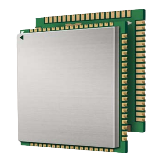
- Page 1 M50Hardware Design Quectel Cellular Engine Hardware Design M50_HD_V2.0 M50_HD_V2.0 - 1 -...
- Page 2 M50_HD_V2.0 General Notes Quectel offers this information as a service to its customers, to support application and engineering efforts that use the products designed by Quectel. The information provided is based upon requirements specifically provided for customers of Quectel. Quectel has not undertaken any independent search for additional information, relevant to any information that may be in the customer’s possession.
-
Page 3: Table Of Contents
M50Hardware Design Contents Contents ..............................3 Table Index .............................. 5 Figure Index ............................6 0. Revision history ..........................8 1. Introduction ............................9 1.1. Related documents........................9 1.2. Terms and abbreviations......................10 1.3. Safety cautions ........................12 2. Product concept ..........................15 2.1. - Page 4 M50Hardware Design 3.10.3. Receiver and speaker interface design ..............52 3.10.4. Earphone interface design..................54 3.10.5. Loud speaker interface design ................... 54 3.10.6. Audio characteristics ....................55 3.11. SIM card interface ........................ 55 3.11.1. SIM card application ....................55 3.11.2. 6 Pin SIM cassette ...................... 57 3.11.3.
- Page 5 TABLE 3: MODULE KEY FEATURES ....................15 TABLE 4: CODING SCHEMES AND MAXIMUM NET DATA RATES OVER AIR INTERFACE .. 17 TABLE 5: M50 PIN ASSIGNMENT ..................... 21 TABLE 6: PIN DESCRIPTION ......................22 TABLE 7: OVERVIEW OF OPERATING MODES................29 TABLE 8: PIN DEFINITION OF THE CHARGING ................
- Page 6 M50Hardware Design Figure Index FIGURE 1: MODULE FUNCTIONAL DIAGRAM ................18 FIGURE 2: PIN ASSIGNMENT ......................20 FIGURE 3: VOLTAGE RIPPLE DURING TRANSMITTING ............. 30 FIGURE 4: REFERENCE CIRCUIT FOR THE VBAT INPUT ............31 FIGURE 5: REFERENCE CIRCUIT FOR POWER SUPPLY .............. 31 FIGURE 6: TURN ON THE MODULE USING DRIVING CIRCUIT..........
- Page 7 FIGURE 49: REFERENCE DESIGN FOR RF ..................71 FIGURE 50: RF SOLDERING SAMPLE....................73 FIGURE 51: M50 TOP AND SIDE DIMENSIONS ................79 FIGURE 52: M50 BOTTOM DIMENSIONS ..................80 FIGURE 53: RECOMMENDED FOOTPRINT WITHOUT BOTTOM CENTRE PADS ....81 FIGURE 55: TOP VIEW OF THE MODULE ..................
-
Page 8: Revision History
M50Hardware Design 0. Revision history Revision Date Author Description of change 2011-12-20 Ray XU Initial 2012-02-03 Ray XU 1. Updated PCM interface 2. Updated SD interface 3. Updated charging interface 4. Updated timing of turning on the module 2012-07-20 Baly BAO 1. -
Page 9: Introduction
M50 Hardware Design 1. Introduction This document defines the M50 module and describes the hardware interface of M50 which are connected with the customer application and the air interface. This document can help customers quickly understand module interface specifications, electrical and mechanical details. -
Page 10: Terms And Abbreviations
M50 Hardware Design 1.2. Terms and abbreviations Table 2: Terms and abbreviations Abbreviation Description Analog-to-Digital Converter Adaptive Multi-Rate Antenna Reference Point ASIC Application Specific Integrated Circuit Bit Error Rate Bill Of Material Base Transceiver Station CHAP Challenge Handshake Authentication Protocol... - Page 11 M50 Hardware Design Li-Ion Lithium-Ion Mobile Originated Mobile Station (GSM engine) Mobile Terminated Password Authentication Protocol PBCCH Packet Switched Broadcast Control Channel Printed Circuit Board Protocol Data Unit Point-to-Point Protocol Radio Frequency Root Mean Square (value) Real Time Clock Receive Direction...
-
Page 12: Safety Cautions
Manufacturers of the cellular terminal should send the following safety information to users and operating personnel and to incorporate these guidelines into all manuals supplied with the product. If not so, Quectel does not take on any liability for customer failure to comply with these precautions. - Page 13 EU. 1.4. Directives and standards The M50 module is designed to comply with the FCC statements. FCC ID: XMR201211M50. The Host system using M50, should have label indicated contains FCC ID: XMR201211M50.
- Page 14 M50 Hardware Design The manual of the host system, which uses M50, must include RF exposure warning statement to advice user should keep minimum 20cm from the radio antenna of M50 module depending on the Mobile status. The following list of antenna is indicating the maximum permissible antenna gain.
-
Page 15: Product Concept
It provides abundant hardware interfaces between the module and customer’s host board. Designed with power saving technique, the current consumption of M50 is as low as 1.3 mA in SLEEP mode when DRX is 5. M50 is integrated with Internet service protocols, such as TCP, UDP, FTP and PPP. Extended AT commands have been developed for customer to use these Internet service protocols easily. - Page 16 M50 Hardware Design Temperature range Normal operation: -35°C ~ +80°C Restricted operation: -40°C ~ -35°C and +80°C ~ +85°C Storage temperature: -45°C ~ +90°C DATA GPRS: GPRS data downlink transfer: max. 85.6 kbps GPRS data uplink transfer: max. 85.6 kbps ...
-
Page 17: Functional Diagram
CS-3 15.6kbps 31.2kbps 62.4kbps CS-4 21.4kbps 42.8kbps 85.6kbps 2.2. Functional diagram The following figure shows a block diagram of the M50 module and illustrates the major functional parts: Power management Baseband Serial Flash The radio frequency part ... -
Page 18: Evaluation Board
Figure 1: Module functional diagram 2.3. Evaluation board In order to help customer to develop applications with M50 , Quectel supplies an evaluation board (EVB), RS-232 to USB cable, power adapter, earphone, antenna and other peripherals to control or test the module. For details, please refer to the document [12]. -
Page 19: Application Interface
M50 Hardware Design 3. Application interface The module is equipped with 83-pin SMT pads and it adopts LCC package. Detailed descriptions on Sub-interfaces included in these pads are given in the following chapters: Power supply Power on/down ... -
Page 20: Pin Of Module
M50 Hardware Design 3.1. Pin of module 3.1.1. Pin assignment ADC1 SIM1_VDD ADC0 SIM1_DATA Top view RESERVED SIM1_CLK NETLIGHT SIM1_RST SPK2P SIM1_GND AGND MIC2P MIC2N RESERVED MIC1P MIC1N RESERVED SPK1N RESERVED SPK1P LOUDSPKN RESERVED RESERVED LOUDSPKP DBG_RXD STATUS DBG_TXD RXD_AUX... -
Page 21: Table 5: M50 Pin Assignment
M50 Hardware Design Table 5: M50 pin assignment 管脚号 管脚名 输入/输出 管脚号 管脚名 输入/输出 ADC1 ADC0 RESERVED NETLIGHT SPK2P AGND MIC2P MIC2N MIC1P MIC1N SPK1N SPK1P LOUDSPKN LOUDSPKP STATUS PWRKEY EMERG_OFF PCM_IN PCM_CLK PCM_OUT PCM_SYNC RESERVED RESERVED RESERVED RESERVED RESERVED... -
Page 22: Pin Description
M50 Hardware Design RESERVED RESERVED RESERVED RESERVED RESERVED RESERVED Note: Keep all reserved pins open. 3.1.2. Pin description Table 6: Pin description Power supply PIN NAME DESCRIPTION COMMENT CHARACTERISTICS VBAT Main power supply Vmax= 4.6V Make sure that of module: Vmin=3.3V... - Page 23 M50 Hardware Design Turn on/off PIN NAME DESCRIPTION COMMENT CHARACTERISTICS PWRKEY Turn on/off control. VILmax= Pulled up to PWRKEY should be 0.1×VBAT VBAT internally. pulled down for a VIHmin= moment to turn on 0.6×VBAT or off the system. VImax=VBAT Emergency shutdown...
- Page 24 M50 Hardware Design MIC2P 7, 8 Channel two for MIC2N positive and negative voice-band input SPK1P 12, 11 Channel one for 1. If unused, SPK1N positive and keep these pins negative voice-band open. output 2. Support both voice and SPK2P Channel two for ringtone output.
- Page 25 M50 Hardware Design 0.15×VDD_EXT Debug Port PIN NAME DESCRIPTION COMMENT CHARACTERISTICS DBG_TXD UART interface for VILmin=0V If unused, keep debugging only. VILmax= these pins open. 0.25×VDD_EXT VIHmin= 0.75×VDD_EXT DBG_RXD VIHmax= VDD_EXT+0.3 VOHmin= 0.85×VDD_EXT VOLmax= 0.15×VDD_EXT Auxiliary UART Port PIN NAME...
- Page 26 M50 Hardware Design 0.15×SIM_VDD holder. VOHmin= SIM_VDD-0.4 SIM_CLK SIM clock 3V: VOLmax=0.4 VOHmin= 0.9×SIM_VDD 1.8V: VOLmax= 0.12×SIM_VDD VOHmin= 0.9×SIM_VDD SIM_RST SIM reset 3V: VOLmax=0.36 VOHmin= 0.9×SIM_VDD 1.8V: VOLmax= 0.2×SIM_VDD VOHmin= 0.9×SIM_VDD SIM_GND SIM ground SIM_PRESEN SIM card detection VILmin=0V If unused, keep VILmax= this pin open.
- Page 27 M50 Hardware Design PCM_OUT PCM data output 0.25×VDD_EXT VIHmin= PCM_SYNC PCM frame 0.75×VDD_EXT synchronization VIHmax= VDD_EXT+0.3 VOHmin= 0.85×VDD_EXT VOLmax= 0.15×VDD_EXT SD card PIN NAME DESCRIPTION COMMENT CHARACTERISTICS SD_CMD SD command VILmin=0V VILmax= SD_CLK SD clock 0.25×VDD_EXT SD_DATA0 SD data VIHmin= 0.75×VDD_EXT...
- Page 28 M50 Hardware Design M50_HD_V2.0 - 28 -...
-
Page 29: Operating Modes
M50 Hardware Design 3.2. Operating modes The table below briefly summarizes the various operating modes in the following chapters. Table 7: Overview of operating modes Mode Function Normal operation GSM/GPRS The module will automatically go into SLEEP mode if DTR... -
Page 30: Power Supply
For the M50 module, the max current consumption could reach to 1.6A during a transmit burst. It will cause a large voltage drops on the VBAT. In order to ensure stable operation of the module, it is recommended that the max voltage drop during the transmit burst does not exceed 400mV. -
Page 31: Reference Design For Power Supply
M50 Hardware Design VBAT 100uF 100nF 10pF 33pF 0603 0603 Figure 4: Reference circuit for the VBAT input 3.3.3. Reference design for power supply The power design for the module is very important, since the performance of power supply for the module largely depends on the power source. -
Page 32: Monitor Power Supply
M50 Hardware Design 3.3.4. Monitor power supply To monitor the supply voltage, customer can use the “AT+CBC” command which includes three parameters: charging status, remaining battery capacity and voltage value (in mV). It returns the 0~100 percent of battery capacity and actual value measured between VBAT and GND. The voltage is automatically measured in period of 5s. -
Page 33: Figure 8: Timing Of Turning On System
M50 Hardware Design The other way to control the PWRKEY is using a button directly. A TVS component is indispensable to be placed nearby the button for ESD protection. When pressing the key, electrostatic strike may generate from finger. A reference circuit is shown in the following figure. -
Page 34: Power Down
M50 Hardware Design 3.4.2. Power down The following procedures can be used to turn off the module: Normal power down procedure: Turn off module using the PWRKEY pin Normal power down procedure: Turn off module using command “AT+QPOWD”... - Page 35 M50 Hardware Design STATUS pin, which is a low level voltage in this mode. 3.4.2.2. Power down module using AT command Customer’s application can turn off the module via AT command “AT+QPOWD=1”. This command will let the module to log off from the network and allow the firmware to save important data before completely disconnecting the power supply, thus it is a safe way.
-
Page 36: Restart
M50 Hardware Design correctly synchronized after start-up. The module is recommended to set to a fixed baud rate. After that moment, no further AT commands can be executed. The module logs off from network and enters power down mode, and only RTC is still active. The power down mode can also be indicated by the pin STATUS, which is a low level voltage in this mode. -
Page 37: Figure 12: Timing Of Restarting System
M50 Hardware Design least 500ms should be delayed after detecting the low level of STATUS. The restart timing is illustrated as the following figure. Delay >0.5s Restart Turn off PWRKEY (INPUT) Pull down the PWRKEY STATUS to turn on the module... -
Page 38: Charge Interface
M50 Hardware Design 3.5. Charge interface M50 provides charging function for rechargeable Li-Ion or Lithium Polymer battery. It is introduced simply in this document. If customer wants to get more information about charging, please refer to the document [13]. Table 8: Pin definition of the charging Name Description. -
Page 39: Sleep Mode
M50 Hardware Design “AT+CFUN=1”. For detailed information about “AT+CFUN”, please refer to the document [1]. 3.6.2. SLEEP mode The SLEEP mode is disabled in default firmware configuration. Customer’s application can enable this mode by “AT+QSCLK=1”. On the other hand, the default setting is “AT+QSCLK=0”... -
Page 40: Rtc Backup
M50 Hardware Design 3.8. RTC backup The RTC (Real Time Clock) can be supplied by an external capacitor or battery (rechargeable or non-chargeable) through the pin VRTC. A 1.5K resistor has been integrated in the module for current limiting. A coin-cell battery or a super-cap can be used to backup power supply for RTC. -
Page 41: Serial Interfaces
M50 Hardware Design Coin-type rechargeable capacitor such as XH414H-IV01E from Seiko can be used. Figure 17 : Seiko XH414H-IV01E Charge Characteristics 3.9. Serial interfaces The module provides three serial ports: UART Port, Debug Port and Auxiliary UART Port. The module is designed as a DCE (Data Communication Equipment), following the traditional DCE-DTE (Data Terminal Equipment) connection. -
Page 42: Uart Port
M50 Hardware Design The Debug Port DBG_TXD: Send data to the COM port of computer. DBG_RXD: Receive data from the COM port of computer. The Auxiliary UART Port TXD_AUX: Send data to the RXD of DTE. ... - Page 43 M50 Hardware Design Used for AT command, GPRS data, etc. Multiplexing function is supported on the UART Port. So far only the basic mode of multiplexing is available. Support the communication baud rates as the following: 300, 600, 1200, 2400, 4800, 9600, 14400, 19200, 28800, 38400, 57600, 115200.
- Page 44 M50 Hardware Design 3.9.1.2. The connection of UART The connection between module and host using UART Port is very flexible. Three connection styles are illustrated as below. Reference design for Full-Function UART connection is shown as below when it is applied in modulation-demodulation.
-
Page 45: Figure 20: Reference Design For Uart Port With Hardware Flow Control
M50 Hardware Design UART Port with hardware flow control is shown as below. This connection will enhance the reliability of the mass data communication. Host (DTE) Module (DCE) Controller Figure 20 : Reference design for UART Port with hardware flow control 3.9.1.3. -
Page 46: Debug Port
M50 Hardware Design 3.9.2. Debug Port Debug Port Two lines: DBG_TXD and DBG_RXD It outputs log information automatically. Debug Port is only used for firmware debugging and its baud rate must be configured as 460800bps. Module (DCE) -
Page 47: Uart Application
M50 Hardware Design Host (DTE) Module (DCE) Controller TXD_AUX RXD_AUX Figure 23: Reference design for Auxiliary UART port 3.9.4. UART application The reference design of 3.3V level match is shown as below. If the host is a 3V system, please change the 5.6K resistor to 15K. -
Page 48: Figure 25: Level Match Design For 5V System
M50 Hardware Design The reference design for 5V level match is shown as below. The connection of dotted line can be referred to the connection of solid line. Please pay attention to the direction of signal. Input dotted line of module should be referred to input solid line of the module. Output dotted line of module should be referred to output solid line of the module. -
Page 49: Figure 26: Level Match Design For Rs-232
M50 Hardware Design The following circuit shows a reference design for the communication between module and PC. Since the electrical level of module is 2.8V, so a RS-232 level shifter must be used. SP3238 T1IN T4OUT T2IN T2OUT T3IN T3OUT... -
Page 50: Audio Interfaces
M50 Hardware Design 3.10. Audio interfaces The module provides two analogy input channels and three analogy output channels. Table 12: Pin definition of Audio interfaces Interface Name Description MIC1P Channel one for Microphone positive input MIC1N Channel one for Microphone negative input... -
Page 51: Decrease Tdd Noise And Other Noise
M50 Hardware Design Table 13: AOUT3 output characteristics Parameter Condition Unit RMS power 8ohm load VBAT=4.3V THD+N=1% 8ohm load VBAT=3.7V THD+N=1% Gain adjustment range Gain adjustment steps 3.10.1. Decrease TDD noise and other noise The 33pF capacitor is applied for filtering out 900MHz RF interference when the module is transmitting at GSM900MHz. -
Page 52: Receiver And Speaker Interface Design
M50 Hardware Design Close to Microphone Differential layout 10pF 33pF 0603 0603 Electret Microphone MICxP 10pF 33pF Module 0603 0603 MICxN 33pF 10pF 0603 0603 Figure 27: Reference design for AIN1&AIN2 3.10.3. Receiver and speaker interface design Close to Speaker... - Page 53 M50 Hardware Design Close to Speaker Differential layout 33pF 10pF 0603 0603 22uF SPK2P Module AGND Figure 29: Handset interface design for AOUT2 Close to Speaker Differential layout Amplifier 33pF 10pF 0603 0603 circuit SPK2P Module AGND 10pF 33pF 0603...
-
Page 54: Earphone Interface Design
M50 Hardware Design 3.10.4. Earphone interface design Close to Socket Differential layout 4.7uF 10pF 33pF MIC2N 0603 0603 MIC2P Module 22uF SPK2P AGND 10pF 33pF 0603 0603 Amphenol 9001-8905-050 AGND AGND Figure 31: Earphone interface design 3.10.5. Loud speaker interface design... -
Page 55: Audio Characteristics
M50 Hardware Design 3.10.6. Audio characteristics Table 14: Typical electret microphone characteristics Parameter Unit Working Voltage Working Current External Microphone Load Resistance kOhm Table 15: Typical speaker characteristics Parameter Unit Normal Single Load Output Ended Resistance (AOUT1) Ref level Differential... -
Page 56: Table 16: Pin Definition Of The Sim Interface
M50 Hardware Design Table 16: Pin definition of the SIM interface Name Description SIM_VDD Supply power for SIM Card. Automatic detection of SIM card voltage. 3.0V±10% and 1.8V±10%. Maximum supply current is around 10mA. SIM_DATA SIM data SIM_CLK SIM clock... -
Page 57: Pin Sim Cassette
M50 Hardware Design Note: Please do not use “AT+QSIMDET=1,1” which causes to initialize SIM card when Figure 33 circuit is adopted. If customer does not need the SIM card detection function, keep SIM_PRESENCE open. The reference circuit using a 6-pin SIM card socket is illustrated as the following figure. -
Page 58: Pin Sim Cassette
M50 Hardware Design Figure 35 : Amphenol C707 10M006 512 2 SIM card holder Table 17: Pin description of Amphenol SIM card holder Name Description SIM_VDD SIM Card Power Supply SIM_RST SIM Card Reset SIM_CLK SIM Card Clock Ground Not Connect... -
Page 59: Table 18: Pin Description Of Molex Sim Card Holder
M50 Hardware Design Figure 36 : Molex 91228 SIM card holder Table 18: Pin description of Molex SIM card holder Name Description SIM_VDD SIM Card Power supply SIM_RST SIM Card Reset SIM_CLK SIM Card Clock SIM_PRESENCE C4 SIM Card Presence Detection... -
Page 60: Sd Card Interface
M50 Hardware Design 3.12. SD card interface The module provides SD card interface that support many types of memory, such as Memory Stick, SD/MCC card and T-Flash or Micro SD card. The following are the main features of SD card interface. -
Page 61: Table 20: Pin Name Of The Sd Card And Micro Sd Card
M50 Hardware Design Table 20: Pin name of the SD card and Micro SD card Pin NO. Pin name of SD card Pin name of T-Flash(Micro SD) card CD/DATA3 DATA2 CD/DATA3 VSS1 VSS2 DATA0 DATA0 DATA1 DATA1 DATA2 In SD card interface designing, in order to ensure good communication performance with SD card, the following design principles should be complied with. -
Page 62: Pcm Interface
PCM frame synchronization 3.13.1. Configuration M50 supports 16 bits line code PCM format. The sample rate is 8 KHz, the clock source is 256 KHz, and the module can only act as master mode. The PCM interfaces support long and short synchronization simultaneously. -
Page 63: Timing
The sample rate of the PCM interface is 8 KHz and the clock source is 256 KHz, so every frame contains 32 bits data, since M50 supports 16 bits line code PCM format, the left 16 bits are invalid. The following diagram shows the timing of different combinations. The synchronization length in long synchronization format can be programmed by firmware from one bit to eight bits. -
Page 64: Reference Design
12 11 10 Zero padding Figure 41: Short synchronization & Zero padding diagram 3.13.3. Reference design As M50 only acts as a master, the module provides synchronization and clock source. The reference design is shown as below. Module Codec (master) -
Page 65: Table 23: Qpcmon Command Description
M50 Hardware Design Table 23: QPCMON command description Parameter scope Description Mode 0: Close PCM 1: Open PCM 2: Open PCM when audio talk is set up Sync_Type 0: Short synchronization 1: Long synchronization Sync_Length Programmed from one bit to eight bit... -
Page 66: Adc
M50 Hardware Design 3.14. ADC The module provides two ADC channel to measure the value of voltage. Please give priority to the use of ADC0 channel. The command “AT+QADC” can read the voltage value applied on ADC0 pin, while AT command “AT+QEADC” can read the voltage value applied on ADC1 pin. For details of this AT command, please refer to the document [1]. -
Page 67: Figure 45: Ri Behavior As A Caller
M50 Hardware Design 4. Change to HIGH when SMS is received. When a new SMS comes, the RI changes to LOW and holds low level for about 120 ms, then changes to HIGH. Certain URCs can trigger 120ms low level on RI. For more details, please refer to the document [1] If the module is used as a caller, the RI would maintain high except the URC or SMS is received. -
Page 68: Figure 46: Ri Behavior Of Urc Or Sms Received
M50 Hardware Design 120ms HIGH Idle or URC or Talking SMS received Figure 46: RI behavior of URC or SMS received M50_HD_V2.0 - 68 -... -
Page 69: Network Status Indication
M50 Hardware Design 3.16. Network status indication The NETLIGHT signal can be used to drive a network status indicator LED. The working state of this pin is listed in the following table. Table 28: Working state of the NETLIGHT State Module function The module is not running. -
Page 70: Figure 48: Reference Design For Status
M50 Hardware Design VBAT 300R Module 4.7K STATUS Figure 48 : Reference design for STATUS M50_HD_V2.0 - 70 -... -
Page 71: Antenna Interface
Figure 49 : Reference design for RF M50 provides an RF antenna pad for customer’s antenna connection. The RF trace in host PCB connected to the module RF antenna pad should be micro-strip line or other types of RF trace, whose characteristic impedance should be close to 50Ω. -
Page 72: Rf Output Power
M50 Hardware Design GSM850/EGSM900 is <1dB. DCS1800/PCS1900 is <1.5dB. 4.2. RF output power Table 31: The module conducted RF output power Frequency GSM850 32.5dBm ±1dB 5dBm±5dB EGSM900 32.5dBm ±1dB 5dBm±5dB DCS1800 29.5dBm ±1dB 0dBm±5dB PCS1900 29.5dBm ±1dB 0dBm±5dB Note: In GSM850&EGSM900 GPRS 4 slots TX mode, the max output power is reduced by... -
Page 73: Rf Cable Soldering
M50 Hardware Design 4.5. RF cable soldering Soldering the RF cable to RF pad of module correctly will reduce the loss on the path of RF, please refer to the following example of RF soldering. Figure 50: RF soldering sample M50_HD_V2.0... -
Page 74: Electrical, Reliability And Radio Characteristics
M50 Hardware Design 5. Electrical, reliability and radio characteristics 5.1. Absolute maximum ratings Absolute maximum ratings for power supply and voltage on digital and analog pins of module are listed in the following table: Table 34: Absolute maximum ratings Parameter... -
Page 75: Power Supply Ratings
M50 Hardware Design 5.3. Power supply ratings Table 36: The module power supply ratings Parameter Description Conditions Min Typ Unit VBAT Supply Voltage must stay within the voltage min/max values, including voltage drop, ripple, and spikes. V drop during Maximum power control level transmitting on GSM850 and GSM900. -
Page 76: Current Consumption
M50 Hardware Design DCS1800/PCS1900 420/470 Peak supply Maximum power control level current on GSM850 and GSM900. (during transmission slot) Power control level PCL 5 Power control level PCL 0 5.4. Current consumption The values of current consumption are shown as below. - Page 77 M50 Hardware Design DATA mode, GPRS ( 3 Rx, 2 Tx ) CLASS 12 GSM850 @power level #5 <550mA,Typical 435mA @power level #12,Typical 158mA @power level #19,Typical 99mA EGSM 900 @power level #5 <550mA,Typical 400mA @power level #12,Typical 150mA @power level #19,Typical 97mA DCS 1800 @power level #0 <450mA,Typical 313mA...
-
Page 78: Electro-Static Discharge
M50 Hardware Design EGSM 900 @power level #5 <660mA,Typical 560mA @power level #12,Typical 215mA @power level #19,Typical 114mA DCS 1800 @power level #0 <530mA,Typical 420mA @power level #7,Typical 173mA @power level #15,Typical 97mA PCS 1900 @power level #0 <530mA,Typical 470mA... -
Page 79: Mechanical Dimensions
M50 Hardware Design 6. Mechanical dimensions This chapter describes the mechanical dimensions of the module. 6.1. Mechanical dimensions of module Figure 51: M50 top and side dimensions M50_HD_V2.0 - 79 -... -
Page 80: Figure 52: M50 Bottom Dimensions
M50 Hardware Design Figure 52: M50 bottom dimensions M50_HD_V2.0 - 80 -... -
Page 81: Recommended Footprint Without Bottom Centre Pads
M50 Hardware Design 6.2. Recommended footprint without bottom centre pads frame line silkscreen Figure 53: Recommended footprint without bottom centre pads M50_HD_V2.0 - 81 -... -
Page 82: Top View Of The Module
M50 Hardware Design 6.4. Top view of the module Figure 54: Top view of the module M50_HD_V2.0 - 82 -... -
Page 83: Bottom View Of The Module
M50 Hardware Design 6.5. Bottom view of the module Figure 55 : Bottom view of the module M50_HD_V2.0 - 83 -... -
Page 84: Storage And Manufacturing
7. Storage and manufacturing 7.1. Storage M50 is distributed in vacuum-sealed bag. The restriction of storage condition is shown as below. Shelf life in sealed bag: 12 months at <40℃/90% RH After this bag is opened, devices that will be subjected to reflow solder or other high temperature process must be: Mounted within 72 hours at factory conditions of ≤30℃/60% RH... -
Page 85: Soldering
PCB. The force on the squeegee should be adjusted so as to produce a clean stencil surface on a single pass. To ensure the module soldering quality, the thickness of stencil at the hole of the module pads should be 0.2mm for M50 . Figure 56: Paste application Suggest peak reflow temperature is from 235℃... -
Page 86: Packaging
Figure 57: Ramp-Soak-Spike reflow profile 7.3. Packaging M50 modules are distributed in trays of 20 pieces each. This is especially suitable for the M50 according to SMT processes requirements. The trays are stored inside a vacuum-sealed bag which is ESD protected. It should not be opened until the devices are ready to be soldered onto the application. -
Page 87: Appendix A: Gprs Coding Schemes
M50 Hardware Design Appendix A: GPRS coding schemes Four coding schemes are used in GPRS protocol. The differences between them are shown in Table 39. Table 39: Description of different coding schemes Scheme Code USF Pre-coded Radio Tail Coded Punctured... -
Page 88: Appendix B: Gprs Multi-Slot Classes
M50 Hardware Design Appendix B: GPRS multi-slot classes Twenty-nine classes of GPRS multi-slot modes are defined for MS in GPRS specification. Multi-slot classes are product dependant, and determine the maximum achievable data rates in both the uplink and downlink directions. Written as 3+1 or 2+2, the first number indicates the amount of downlink timeslots, while the second number indicates the amount of uplink timeslots. - Page 89 Shanghai Quectel Wireless Solutions Co., Ltd. Room 501, Building 13, No.99 Tianzhou Road, Shanghai, China 200233 Tel: +86 21 5108 6236 Mail: info@quectel.com...
Need help?
Do you have a question about the M50 and is the answer not in the manual?
Questions and answers