Table of Contents
Advertisement
Quick Links
MITSUBISHI
CAUTION
Before servicing this chassis, it is important that the service person reads the "SAFETY PRECAUTIONS" and "PRODUCT
SAFETY NOTICE" in this service manual.
• Power Input
: AC 100 - 240 V ; 50 / 60 Hz
• Rated Input
: 2.3 A
• LCD Panel
: 0.7 inch LCD panel: 3 pieces (for R,G,B)
Active pixel rate: 99.99 % or more (each panel)
Pixels 800 × 600 = 480,000 pixels
[SL1U]
Total 1,440,000 pixels
Pixels 1,024 × 768 = 786,432 pixels
[XL1U]
Total 2,359,296 pixels
• Colors
: 16,770,000 colors
• Projection Lens
: F 1.9 - 2.2 f = 27.0 - 32.0 mm
• Light Source Lamp
: 150 W NSH
• Picture Size
: aspect ratio 4:3 30 - 300 inch
• PC compatibility
:
Resolution : 640 × 400 - 800 × 600 + Compressed
[SL1U]
1,024 × 768 Sync on Green available
Resolution : 640 × 400 - 1,024 × 768 + Compressed
[XL1U]
1,280 × 1,024 Sync on Green available
• Video compatibility
: NTSC/NTSC4.43/PAL(including PAL-M,N)
/SECAM, PAL-60 DVD(Component)/
HDTV(1080i)/720p/(525p)
: Round type (8 Ω 1 W)
• Speaker
• Audio Output
: 1 W mono
• Audio Input
: 350 mV(rms), 10 kΩ or more
Copyright C 2001 Mitsubishi Electric Corporation All Rights Reserved.
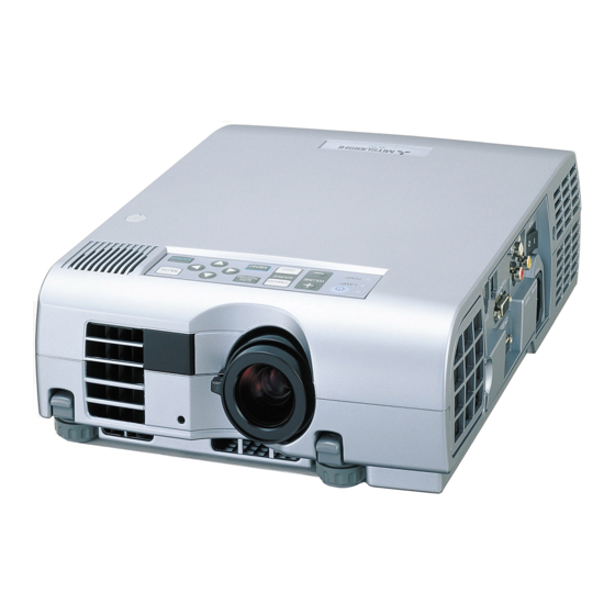
MODEL
SL1U / XL1U
SPECIFICATIONS
MITSUBISHI ELECTRIC
LCD PROJECTOR
LC31 CHASSIS [SL1U]
LC29 CHASSIS [XL1U]
: Luminance signal: 1.0 V(p-p) 75 Ω
• S-Video Input
Chroma signal: 0.286 V(p-p) 75 Ω
: 1.0 V(p-p) 75 Ω (negative sync.)
• Video Input
: RGB : 0.7 V(p-p) 75 Ω (negative sync.)
• Analog RGB Input
(mini D-SUB 15P)
YC
C
HD/CS: TTL level (positive or negative)
VD: TTL level (positive or negative)
• Control connector
:
[SL1U]
Serial (DIN 8 pin female connector)
RS-232C standards
[XL1U]
Serial (DIN 8 pin female connector)
RS-232C standards
USB terminal for mouse
: 9.3"(W) × 3.7"(H) × 12.4"(D)
• Cabinet
(237 × 94 × 315 mm)
Dimensions
(Legs and lens are included.)
• Weight
: Approx. 2.9 kg (6.5 lbs)
• Length of Power Cord
: 9.5 feet (2.9 m)
• Weight and dimensions shown are approximate.
• Design and specifications are subject to change without notice.
(negative sync.)
(burst signal)
C
Y : 1.0 V(p-p) (negative sync.)
B
R
C
:
0.7 V(p-p)
B
R
2001
Advertisement
Table of Contents

Related Manuals for Mitsubishi SL1U


Summary of Contents for Mitsubishi SL1U
-
Page 1: Specifications
: 1 W mono • Weight and dimensions shown are approximate. • Audio Input : 350 mV(rms), 10 kΩ or more • Design and specifications are subject to change without notice. MITSUBISHI ELECTRIC Copyright C 2001 Mitsubishi Electric Corporation All Rights Reserved. -
Page 2: Table Of Contents
CONTENTS – FILE “COVERPGE” – SPECIFICATIONS ···································································································································· CONTENTS ··········································································································································· – FILE “EXPOSED” – TRADEMARK, REGISTERED TRADEMARK ·························································································· PRODUCT SAFETY NOTICE ·················································································································· SAFETY PRECAUTIONS························································································································· PCBs LOCATION ····································································································································· EXPOSED VIEW ······································································································································ DISASSEMBLY ········································································································································ LEAD DRESS··········································································································································· PACKING ··········································································································································· – FILE “MAINTENA” – LAMP REPLACEMENT···························································································································· MAINTENANCE ·······································································································································... -
Page 3: Trademark, Registered Trademark
TRADEMARK, REGISTERED TRADEMARK Apple, Macintosh are registered trademarks of Apple Computer Inc. IBM, VGA, PS/2 are trademarks or registered trademarks of International Business Machines Corporation. Microsoft Windows 95 is a registered trademark of Microsoft in the U.S. and other countries. Space Pointer is registered trademarks of ALPS ELECTRIC CO., LTD. -
Page 4: Safety Precautions
SAFETY PRECAUTIONS North America NOTICE: Observe all cautions and safety related notes located inside the cabinet and on the chassis. WARNING 1. Operation of this LCD PROJECTOR outside the cabinet or with the cover removed presents a shock hazard from the LCD PROJECTOR power supplies. -
Page 5: Pcbs Location
PCBs LOCATION Fig. 1 Parts List : See Parts List Page 2. Item No. Parts Name POWER PCB ASSY LAMP POWER UNIT PREAMP PCB ASSY INLET PCB ASSY TERMINAL PCB ASSY MAIN PCB ASSY AUDIO PCB ASSY SENSOR PCB ASSY Table. -
Page 6: Exposed View
EXPOSED VIEW LVP ASSY Note: Technicians must put on a wrist band to protect LCD panel against Static electricity during the repairs. Parts List : See Parts List Page 3. Parts Name Number of Screws q Top Case Assy A x6 w Membrane Switch B x3 A x6... - Page 7 B x2, G x1 w INLET PCB ASSY I x1 (Washer) e MAIN PCB ASSY C x2, D x2 E x1 [SL1U], E x2 [XL1U] r Terminal Shield t Cooling Fan (Power) F x2, H x1 6 Inlet Barrier none...
- Page 8 POWER ASSY Part AUDIO ASSY Part A x2 Fig. 2-4 Parts List : See Parts List Page 4. Parts Name Number of Screws q Audio Barrier none Fig. 2-3 w AUDIO PCB ASSY none e Audio Holder none Parts List : See Parts List Page 4. Table 2-4 Parts Name Number of Screws...
- Page 9 OPTICAL UNIT Part Note: Technicians must put on a wrist band to protect LCD panel against Static electricity during the repairs. B x1 L x1 C x1 F x5 A x4 E x2 I x1 D x1 J x1 M x1 K x1 G x2 H x1...
- Page 10 OPTICAL UNIT Part Note: Directions of setting parts of !7 to @0 as shown in the pictorial below. Fig. 2-7 Directions which the setting parts face in Light source side (Lamp side) !8 ! 9 @ 0 Flat surface Flat surface RGB Marking shaved edge Uneven surface...
-
Page 11: Disassembly
DISASSEMBLY 1. Removal of TOP CASE ASSY and SPEAKER 1. Remove the seven (a) screws and the Top Case Assy and the Terminal Board as shown in Fig. 3-1. Top Case Assy a x6 Note: Also remove the ST connector on the MAIN PCB Terminal Board ASSY and the GE connector on the AUDIO PCB ASSY when removing the Top Case Assy. - Page 12 3. Removal of PREAMP PCB ASSY and LAMP POWER UNIT a x2 PREAMP PCB ASSY 1. Remove the Top Case Assy and the Terminal Board d x1 c x2 following “1.Removal of TOP CASE ASSY and LAMP POWER UNIT SPEAKER”. (Fig. 3-1) 2.
- Page 13 3. Remove the two (a) screws, (b) screw, two (c) screws and MAIN PCB ASSY as shown in Fig. 3-5-1. Note: The number of screws b is follows: INLET PCB ASSY SL1U 1 screw TERMINAL PCB ASSY XL1U 2 screws Terminal Shield 4.
- Page 14 6. Removal of POWER ASSY 1. Remove the Top Case Assy and the Terminal Board a x2 following “1.Removal of TOP CASE ASSY and SPEAKER”. (Fig. 3-1) Power Assy 2. Remove the Terminal Assy (MAIN PCB ASSY, INLET PCB ASSY, and TERMINAL PCB ASSY) following “4.Removal of TERMINAL ASSY (MAIN PCB ASSY, INLET PCB ASSY, and TERMINAL PCB ASSY) ”.
- Page 15 8. Removal of OPTICAL UNIT 1. Remove the Top Case Assy and the Terminal Board following “1.Removal of TOP CASE ASSY and SPEAKER”. (Fig. 3-1) b x4 2. Remove the Terminal Assy (MAIN PCB ASSY, INLET Optical Unit PCB ASSY, and TERMINAL PCB ASSY) following “4.Removal of TERMINAL ASSY (MAIN PCB ASSY, INLET PCB ASSY, and TERMINAL PCB ASSY) ”.
- Page 16 9. Removal of COOLING FAN UNIT ASSY (PBS) and COOLING FAN UNIT ASSY Cooling Fan Unit Assy (PBS) (EXHAUST) 1. Remove the Top Case Assy and the Terminal Board following “1.Removal of TOP CASE ASSY and Optical Unit a x1 SPEAKER”.
-
Page 17: Removal Of Lcd Block
11. Removal of LENS UNIT 1. Remove the Top Case Assy and the Terminal Board following “1.Removal of TOP CASE ASSY and SPEAKER”. (Fig. 3-1) Optical Unit 2. Remove the Terminal Assy (MAIN PCB ASSY, INLET PCB ASSY, and TERMINAL PCB ASSY) following “4.Removal of TERMINAL ASSY (MAIN PCB ASSY, INLET PCB ASSY, and TERMINAL PCB ASSY) ”. - Page 18 13. Removal of LAMP BOX ASSY Optical Unit 1. Remove the Top Case Assy and the Terminal Board following “1.Removal of TOP CASE ASSY and SPEAKER”. (Fig. 3-1) 2. Remove the Terminal Assy (MAIN PCB ASSY, INLET PCB ASSY, and TERMINAL PCB ASSY) following “4.Removal of TERMINAL ASSY (MAIN PCB ASSY, INLET PCB ASSY, and TERMINAL PCB ASSY) ”.
-
Page 19: Lead Dress
LEAD DRESS Note: 1. The inner wires are clamped so that they do not come close to heat generating or high voltage parts. After servicing route all wires in their original position. 2. Technicians must put on a wrist band to protect LCD panel against Static electricity during the repairs. 1. -
Page 20: Packing
PACKING !1 ! 2 ! 3 ! 4 Put the packages in the packing case !5 ! 6 ! 7 ! 8 Fold the sections shown yuio!0 inside and close the packing case Place the soft case between the folded sections inside. -
Page 21: Electrical Adjustments
ELECTRICAL ADJUSTMENTS Use communication program [Hyper Terminal] of Microsoft ® Windows ® 95 Operating system for every circuit adjustment of this product. Either Windows ® 95 or Windows ® 98 can be applied to the ones described as Microsoft ® Windows ®... - Page 22 ¢ ¢ Adjustment with Microsoft ® Windows ® 95 Operating System 1. Starting 1. Start Windows 2. Double click [Accessories] holder. 3. Double click [Hyper Terminal] holder. 4. Double click [HyperTrm] icon. 2. Hyper Terminal Setting 1. Click [Properties] in File menu on the Hyper Item Setting Terminal window.
- Page 23 Adjustment Procedures [A/D Pre-Amplification Circuit] Adjustment purpose To set amplitude of a video signal to be entered to A/D converter. 1. A/D Convertor Symptom when Incorrectly displayed white portions. incorrectly adjusted Measuring * Enter the adjustment command in capital alphanumeric letters. instrument ...
- Page 24 [Liquid Crystal Panel Adjustment purpose To remove ghosts from the screen. Driving Adjustment Circuit] 2. Ghost (SL1U) Symptom when Ghosts appear. incorrectly adjusted Measuring * Make this adjustment only when ghosts remarkably appear on the screen. instrument * Enter the adjustment command with capital alphanumeric letters.
- Page 25 [Liquid Crystal Panel Adjustment purpose To remove ghosts from the screen. Driving Adjustment Circuit] 2. Ghost (XL1U) Symptom when Ghosts appear. incorrectly adjusted Measuring * Make this adjustment only when ghosts remarkably appear on the screen. instrument * Enter the adjustment command with capital alphanumeric letters. Test point ...
- Page 26 [Liquid Crystal Panel Adjustment purpose To remove flickers form the screen. Driving Adjustment Circuit] 3. Flicker Symptom when Flickers appear. incorrectly adjusted Measuring * Make this adjustment only when flickers remarkably appear on the screen. instrument * Enter the adjustment commands and adjustment values of the hexadecimal number in capital alphanumeric letters.
-
Page 27: Diagnosis Information
DIAGNOSIS INFORMATION Outline of self-diagnosis function This product is provided with the self-diagnosis function. In case of any abnormality, the LED at the top of the product will indicate the errors. There are 2 ways for diagnosis. 1 Connect a personal computer to the product. Then, input [00 ~ CHK] from the hyper-terminal window of the personal computer during stand-by. - Page 28 : LED off Orange : Both Red and Green light Red flash N : The cycle that Red flashes N times and goes out for fixed time is repeated. LED Indication Check Point Preferen- Symptom Failure Reset tial order POWER LAMP TEMP Reference...
-
Page 29: Diagnostic Software, To Read Warning History ( Pcgce Ver.8 )
Select “XL1U” when Warning History 2: The second oldest warning history data using “XL1U” or “SL1U” when using are stored in the Warning History 2. “SL1U”. Warning History 3: The oldest warning history data stored in the Warning History 3. - Page 30 saved when the stand-by power fails during the button to cancel clearing them. stand-by mode. In this case, LED warning indication 5. Pressing the Back button displays the main dialog will appear, so check the error data by the warning window again and carries out communication with the status.) projector again to get information from it.
-
Page 31: Specification Of Rgb Signals In Each Computer Mode Of The Projector
SPECIFICATION OF RGB SIGNALS IN EACH COMPUTER MODE OF THE PROJECTOR [SL1U] resolution horizontal Vertical Normal mode Real mode Signal mode (H x V) frequency (kHz) frequency (Hz) (H x V) (H x V) TV60 15.73 59.94 800 x 600 TV50 15.63... - Page 32 [XL1U] resolution horizontal Vertical Normal mode Real mode Signal mode (H x V) frequency (kHz) frequency (Hz) (H x V) (H x V) TV60 15.73 59.94 1024 x 768 TV50 15.63 50.00 1024 x 768 1080i 33.75 60.00 1024 x 576 720p 45.00 60.00...
-
Page 33: Diagnosis Flow Chart
DIAGNOSIS FLOW CHART Image system Is the lamp lit? Is the indication on LED normal after POWER ON? (POWER : Green, LAMP : Green) An image is not projected properly. Is the proper video signal inputted? Or is the image projected correctly? Malfunction of the drive circuit. - Page 34 Power source system 1 The product does not LED is not lit. enter the stand-by mode. Check STBY5. Check the failure on the PCB- Has the FUSE (F901) POWER, then replace the parts. blown? PCB-INLET Reset the thermal protector Does the thermal thermal protector : on the lamp box and check the dust on the protector work?
- Page 35 Power source system 2 STBY5 Diagnosed as abnormal power source. Insert the lead wire. Or Is RD-SD lead wire OK? replace the lead wire. Remove the SD connector from the PCB-MAIN. Is the voltage on Is the pin No. 6 Malfunction of Z950 or Z951.
- Page 36 Power source system 3 Abnormal power source for SW (SW3.3, SW15.5, SW5A, SW9AU) Are RD-SD, RF-SF, Insert the lead wire. RN-GN and GV-SV lead wires OK? Remove the PCB-MAIN Turn on FAN and POWER and connect the PCB- on the PCB-POWER TEST. POWER TEST.
- Page 37 Power source system 4 The lamp does not light. Are RE-CN1 and SA- Insert or replace them. CN2 lead wires OK? Remove the PCB-MAIN and Turn on FAN and LAMP on connect the PCB-POWER the PCB-POWER TEST. TEST. Is the lamp lit? Malfunction of the PCB-MAIN.
-
Page 38: Control Projector By Using A Personal Computer
LCD Projector XL1U SL1U Control projector by using a personal computer This projector can be controlled by connecting a personal computer with RS-232C terminal. Functions can be controlled by a personal computer: • Turn the ON or OFF • Changing input signals •... - Page 39 3) Control sequence (1) Send the command from a personal computer to the projector. (The commands must be sent at least 400ms apart.) (2) The projector will send a return command 400ms* after it has received an end code. If the command is not received correctly, the projector will not send the return command.
- Page 40 6) Remote commands Some remote control operations can be done by remote command codes. Button's name on remote ASCII + VOLUME – VOLUME KEYSTONE EXPAND MUTE MENU ENTER AUTO POSITION STILL [Example] Display MENU selection bar. (' 'is for ASCII code) Sending commands Status code from Meaning...
- Page 41 VERT LINES 0000 - 9999 VERT.SYNC 0 (AUTO), 1 (ON), 2 (OFF) SHUTTER (U) 000 - 383 (000 - 299 for SL1U) SHUTTER (L) 000 - 383 (000 - 299 for SL1U) SHUTTER (LS) SHLS 000 - 510 (000 - 398 for SL1U)
-
Page 42: Parts List
PARTS LIST MODEL : SL1U / XL1U In order to expedite delivery of replacement part orders. Specify : 1. Model number/Serial number 2. Part number and Description 3. Quantity Unless full information is supplied,delay in execution of orders will result. - Page 43 * ! 4 935C989O01 INLET PCB ASSY * ! 5 935C984O01 TERMINAL PCB ASSY * ! 6 935B267O03 MAIN PCB ASSY [SL1U] * ! 6 935B267O01 MAIN PCB ASSY [XL1U] * ! 7 935C990O01 AUDIO PCB ASSY * ! 8...
- Page 44 The PARTS on this page correspond to ones on page 4 in the EXPOSED file. ITEM PARTS NO. PARTS NAME DESCRIPTION EXPOSED VIEW LVP ASSY (Fig. 2-1) w, 3 975D152O50 TOP CASE ASSY include [SL1U] include w, 3 750A422O10 TOP CASE ASSY [XL1U] 439B001O10 MEMBRANE SWITCH CONTROL SW 480P064O10 SPEAKER 761B381O20...
- Page 45 * ! 1 935C984O01 TERMINAL PCB ASSY * ! 2 935C989O01 INLET PCB ASSY * ! 3 935B267O03 MAIN PCB ASSY [SL1U] * ! 3 935B267O01 MAIN PCB ASSY [XL1U] - - - - - TERMINAL SHIELD 288P227O10 COOLING FAN...
- Page 46 PARTS NO. PARTS NAME DESCRIPTION EXPOSED VIEW OPTICAL UNIT (Fig. 2-6) 499D029O30 LENS CAP 499D029O20 LENS UNIT 499D030O20 LCD BLOCK [SL1U] 499D029O40 LCD BLOCK [XL1U] 499D029O60 THERMISTOR ASSY 499D029O90 THERMAL PROTECTOR 499D030O30 COOLING FAN UNIT ASSY 499D029O80 COOLING FAN UNIT ASSY...
- Page 47 PARTS NO. PARTS NAME DESCRIPTION PACKING 772P037O10 SOFT CASE 803A582O10 PACKING CUSHION 831D190O10 PACKING SHEET 900X900 802B819O30 PACKING CASE [SL1U] 802B819O10 PACKING CASE [XL1U] - - - - - PACKING CASE 6, 11 831D337O10 PACKING BAG 871D341O30 INSTRUCTION BOOK [SL1U] 871D341O10...
-
Page 48: Electrical Parts And Others
ELECTRICAL PARTS AND OTHERS [S] : SL1U [X] : XL1U SYMBOL PARTS SYMBOL PARTS PARTS NAME DESCRIPTION PARTS NAME DESCRIPTION INTEGRATED CIRCUITS TRANSISTORS IC220 270P792O10 IC CLC5633IM Q200 261P005O10 CHIP TRANSISTOR 2SC3123 IC240 275P121O10 MOS IC HD74LVC14T Q201 261P005O10 CHIP TRANSISTOR... - Page 49 [S] : SL1U [X] : XL1U SYMBOL PARTS SYMBOL PARTS PARTS NAME DESCRIPTION PARTS NAME DESCRIPTION D242 264P878O20 CHIP DIODE HZM6.2ZWA D2M0 264P830O20 CHIP DIODE DA204U L5A1 409P865O20 EMI FILTER BLM11A601S L5A2 409P865O20 EMI FILTER BLM11A601S D2M1 264P830O20 CHIP DIODE...
- Page 50 [S] : SL1U [X] : XL1U SYMBOL PARTS SYMBOL PARTS PARTS NAME DESCRIPTION PARTS NAME DESCRIPTION L2C7 325C241O70 CHIP COIL 22µH-K L7M1 103P509O50 CHIP RESISTOR 0Ω(RM1608) L386 325C241O70 CHIP COIL 22µH-K L7M9 103P509O50 CHIP RESISTOR 0Ω(RM1608) L502 325C241O30 CHIP COIL 10µH-K...
- Page 51 [S] : SL1U [X] : XL1U SYMBOL PARTS SYMBOL PARTS PARTS NAME DESCRIPTION PARTS NAME DESCRIPTION R3M0 103P505O50 CHIP RESISTOR 1/16W 330kΩ-J R738 103P500O50 CHIP RESISTOR 1/16W 22Ω-J R3M4 103P505O50 CHIP RESISTOR 1/16W 330kΩ-J R462 103P500O50 CHIP RESISTOR 1/16W 22Ω-J...
- Page 52 [S] : SL1U [X] : XL1U SYMBOL PARTS SYMBOL PARTS PARTS NAME DESCRIPTION PARTS NAME DESCRIPTION R7M2 103P502O50 CHIP RESISTOR 1/16W 1kΩ-J R8A8 103P500O10 CHIP RESISTOR 1/16W 10Ω-J R7M3 103P502O50 CHIP RESISTOR 1/16W 1kΩ-J R8A9 103P500O10 CHIP RESISTOR 1/16W 10Ω-J...
- Page 53 [S] : SL1U [X] : XL1U SYMBOL PARTS SYMBOL PARTS PARTS NAME DESCRIPTION PARTS NAME DESCRIPTION R918 103P471O30 CHIP RESISTOR 1/10W 330Ω-F C288 141P144O60 CHIP CAPACITOR F16/10V 1µF-Z C2E5 141P144O20 CHIP CAPACITOR F16V 0.1µF-Z R919 103P472O50 CHIP RESISTOR 1/10W 1kΩ-F...
- Page 54 [S] : SL1U [X] : XL1U SYMBOL PARTS SYMBOL PARTS PARTS NAME DESCRIPTION PARTS NAME DESCRIPTION C402 141P144O20 CHIP CAPACITOR F16V 0.1µF-Z C4H6 141P144O20 CHIP CAPACITOR F16V 0.1µF-Z C403 181P520O10 CHIP ELE CAPACITOR 6.3V 22µF-M C413 181P528O10 CHIP ELE CAPACITOR 4V 220µF-M...
- Page 55 [S] : SL1U [X] : XL1U SYMBOL PARTS SYMBOL PARTS PARTS NAME DESCRIPTION PARTS NAME DESCRIPTION C508 141P144O30 CHIP CAPACITOR F16V 0.22µF-Z C635 141P144O20 CHIP CAPACITOR F16V 0.1µF-Z C509 181P532O20 CHIP ELE CAPACITOR 16V 4.7µF-M C636 141P144O20 CHIP CAPACITOR F16V 0.1µF-Z...
- Page 56 [S] : SL1U [X] : XL1U SYMBOL PARTS SYMBOL PARTS PARTS NAME DESCRIPTION PARTS NAME DESCRIPTION C7F0 141P140O90 CHIP CAPACITOR B50V 1000pF-K C809 141P144O20 CHIP CAPACITOR F16V 0.1µF-Z C811 141P144O20 CHIP CAPACITOR F16V 0.1µF-Z C7F1 141P140O90 CHIP CAPACITOR B50V 1000pF-K...
- Page 57 [S] : SL1U [X] : XL1U SYMBOL PARTS SYMBOL PARTS PARTS NAME DESCRIPTION PARTS NAME DESCRIPTION C8D7 141P144O20 CHIP CAPACITOR F16V 0.1µF-Z C919 141P135O80 CHIP CAPACITOR F25V 0.1µF-Z C8D9 141P144O20 CHIP CAPACITOR F16V 0.1µF-Z C8E0 141P144O20 CHIP CAPACITOR F16V 0.1µF-Z C920 181P183O10 ELECTROLYTIC CAPACITOR 25V 100µF-M...
- Page 58 [S] : SL1U [X] : XL1U SYMBOL PARTS SYMBOL PARTS PARTS NAME DESCRIPTION PARTS NAME DESCRIPTION 452C247O20 CARD LEAD SOCKET (SG X) 669D522O60 SCREW 2 L=10 452C247O20 CARD LEAD SOCKET (SR S) 683D048O10 WASHER 0.45X4.3X8.5 452C247O20 CARD LEAD SOCKET (SR X)
-
Page 59: Ic Block Diagrams
IC BLOCK DIAGRAMS PCB-MAIN (1/8) IC500 M52036SP CLAMP CLAMP DIGITAL TIMING V.POL. H.POL. VERT S/S IN IC530 HD74LVC14T CLAMP EDGE GEN. FUNCTION TABLE INPUT OUTPUT V.SYNC SEP. LOGIC LOGIC SYNC SEP. HOR. HOR. VERT. VERT. SHAPE SHAPE V.STATE GREEN IN COMP/H VERT IN VERT S/S... - Page 60 IC2A2 SAA7114H 28 29 36 34 35 94 95 81,82, 92 91 96 80 64-67, 32 31 78 77 74 73 44 84-87, 69-72, 89,90, RT out eXpansion port pin mapping I/O control X port I/O formatting chroma of 16 bit input RESON Note: The pins RTCO and ALRCLK...
- Page 61 PCB-MAIN (3/8) IC4G0,IC4H0,IC4J0,IC4S0 A45L9332F-6 MASK REGISTER DQMi CLOCK BLOCK WRITE REGISTER WRITE CONTROL CONTROL LOGIC LOGIC COLUMN (i=0 - 31) MASK DQMi 256K X 32 256K X 32 CELL CELL ARRAY ARRAY ROW DECORDER DQMi BANK SELECTION SERIAL COLUMN ADDRESS REFRESH ADDRESS COUNTER...
- Page 62 10 bit RIN[9:0] ROUT[9:0] γ 10 bit VIDEO PICTURE COLOR REFERENCE CONTRAST CORRECTION GIN[9:0] SIGNAL QUALITY CORRECTION VOLTAGE GOUT[9:0] BRIGHT MASK CONTROL 10 bit BIN[9:0] BOUT[9:0] HPLL HRESETO OSDRIN[1:0] VRESETO OSDGIN[1:0] ENVY1-2 OSDBIN[1:0] DXOUT(R:G:B) OSDSW ENBX1(R:G:B) ENBX2(R:G:B) ENBX3(R:G:B) ENBX4(R:G:B) TIMING CLXOUT(R:G:B) SERIAL SCLK...
- Page 63 PCB-MAIN (5/8) IC5A2 M62358FP N.C. VrefU Gain Determination Latch 8 bit Upper R-2R R-2R R-2R R-2R R-2R Address Segment Decoder R-2R 8 bit Latch 8 bit Latch 8 bit Upper R-2R R-2R R-2R R-2R R-2R Segment R-2R Gain Determination Latch Ao10 Ao11 Ao12...
- Page 64 IC803 L3E01031F0A VCC GND VDD2 DGND 1,13 2,12 46,47 23,37,48 DYIN INVERT LEVEL SHIFT CLYIN LEVEL SHIFT INVERT LEVEL SHIFT DIRYIN LEVEL SHIFT DIRY INVERT LEVEL SHIFT DIRY INVERT LEVEL SHIFT ENBY1IN ENBY1 ENBY2IN INVERT LEVEL SHIFT ENBY2 (VDD2 System) (VDD1 System) DXIN INVERT LEVEL SHIFT...
- Page 65 PCB-MAIN (7/8) IC7A2 HD74LVC14T IC7A3 TC74VHCT32AFT FUNCTION TABLE FUNCTION TABLE INPUT OUTPUT (each gate) INPUTS OUTPUT : HIGH LEVEL : LOW LEVEL IC7H2 SP232ECN +5V to +10V Voltage Doubler +10V to -10V Voltage Inverter 400kΩ T1 IN T1 OUT TTL/CMOS RS-232 400kΩ...
- Page 66 IC901 MC33232D PCB-POWER 1.4V Zero-current detection 5.3V 1.6V /1.4V 2.5V Reference UVLO Timer Output Current detection one-shot 1.5V Overvoltage detection Vref 1.067Vref Mult Multiplier Err Amp Quickstart COMP ON/OFF IC907 LM2594M-5.0 220mV 200mV CURRENT 1.235V 2.5V START SOURCE REFERENCE REGULATOR BIAS COMP.
- Page 67 SCHEMATIC DIAGRAMS MODEL : SL1U XL1U NOTE 1. TP6A, etc. show Test Points. 2. Capacitors pF, for numbers more than 1 Value Not indicated µF, for numbers less than 1 Dielectric Not indicated : 50V Strength ± 10 % Not indicated =...
- Page 68 C3M4 R3M4 D3M1 R2E6 R2E7 C2E9 C2F0 R2G9 R2H0 R2E5 C2E5 TP2A2 R2E3 TP2A1 SL1U/XL1U CONTENTS BLOCK DIAGRAM •••••• q MICROCOM1-MAIN (7/8) •••••• i •••••• w •••••• o AD/DEC-MAIN(1/8) MICROCOM2-MAIN (8/8) TERMINAL •••••• w SENSOR •••••• !0 •••••• e •••••• !0...
- Page 69 C459 R4C5 TPSVD C448 C447 C445 C443 C458 C454 R4C2 R4B8 R4C7 R4C1 C472 SL1U/XL1U CONTENTS BLOCK DIAGRAM •••••• q MICROCOM1-MAIN (7/8) •••••• i •••••• w •••••• o AD/DEC-MAIN(1/8) MICROCOM2-MAIN (8/8) TERMINAL •••••• w SENSOR •••••• !0 •••••• e •••••• !0...
- Page 70 C4H8 C4S5 C4S7 C4G5 C4J7 C4J5 C4H5 C4H7 C4S6 C4G6 C4J6 C4H6 CGCLK SGCLK SL1U/XL1U CONTENTS BLOCK DIAGRAM •••••• q MICROCOM1-MAIN (7/8) •••••• i •••••• w •••••• o AD/DEC-MAIN(1/8) MICROCOM2-MAIN (8/8) TERMINAL •••••• w SENSOR •••••• !0 •••••• e •••••• !0...
- Page 71 C4X3 ENBX2R R4W3 R4W5 DXOUTR R4W2 R4W6 CLXOUTR GSCLK FRPR STSQOR STSQER XFRR SHCLKR SL1U/XL1U CONTENTS BLOCK DIAGRAM •••••• q MICROCOM1-MAIN (7/8) •••••• i •••••• w •••••• o AD/DEC-MAIN(1/8) MICROCOM2-MAIN (8/8) TERMINAL •••••• w SENSOR •••••• !0 •••••• e •••••• !0...
- Page 72 C815 C828 C814 R825 C831 C816 Q803 R839 C829 C830 C844 P831 R840 C837 SL1U/XL1U CONTENTS BLOCK DIAGRAM •••••• q MICROCOM1-MAIN (7/8) •••••• i •••••• w •••••• o AD/DEC-MAIN(1/8) MICROCOM2-MAIN (8/8) TERMINAL •••••• w SENSOR •••••• !0 •••••• e •••••• !0...
- Page 73 R8R0 C8D7 C8Q7 C8E2 C8R2 C8E0 C8R0 C8E4 C8E3 C8R4 C8R3 C8D9 C8Q9 P8Q1 SL1U/XL1U CONTENTS BLOCK DIAGRAM •••••• q MICROCOM1-MAIN (7/8) •••••• i •••••• w •••••• o AD/DEC-MAIN(1/8) MICROCOM2-MAIN (8/8) TERMINAL •••••• w SENSOR •••••• !0 •••••• e •••••• !0...
- Page 74 P7H6 L7M9 R7K7 P7S3 R7P7 P7H7 L7J0 P7S4 R7Q0 R7K8 P7H8 L7J1 P7H9 L7J2 SL1U/XL1U CONTENTS BLOCK DIAGRAM •••••• q MICROCOM1-MAIN (7/8) •••••• i •••••• w •••••• o AD/DEC-MAIN(1/8) MICROCOM2-MAIN (8/8) TERMINAL •••••• w SENSOR •••••• !0 •••••• e •••••• !0...
- Page 75 R750 UCSLD UCSDT UCSCK AU-P-ON DIRX DIRXZ FANON DIRY S-MUTE LAMP-L/H HSTATE VSTATE COMP/S SL1U/XL1U CONTENTS BLOCK DIAGRAM •••••• q MICROCOM1-MAIN (7/8) •••••• i •••••• w •••••• o AD/DEC-MAIN(1/8) MICROCOM2-MAIN (8/8) TERMINAL •••••• w SENSOR •••••• !0 •••••• e •••••• !0...
- Page 76 R926 L908 R939 L907 D903 C930 D905 D904 C933 C931 IC903 IC908 R940 C932 SL1U/XL1U CONTENTS BLOCK DIAGRAM •••••• q MICROCOM1-MAIN (7/8) •••••• i •••••• w •••••• o AD/DEC-MAIN(1/8) MICROCOM2-MAIN (8/8) TERMINAL •••••• w SENSOR •••••• !0 •••••• e •••••• !0...
- Page 77 R386 A – 1 R9B3 C – 5 C9F1 C – 4 J9F1 A – 3 B – 1 C954 B – 4 A – 2 R391 A – 1 R9B4 C – 4 C9F1 C – 5 SL1U XL1U...
Need help?
Do you have a question about the SL1U and is the answer not in the manual?
Questions and answers