
Related Manuals for Winbond W25Q16BV


Summary of Contents for Winbond W25Q16BV
- Page 1 W25Q16BV 16M-BIT SERIAL FLASH MEMORY WITH DUAL AND QUAD SPI Publication Release Date: July 08, 2010 - 1 - Revision F...
-
Page 2: General Description
Pages can be erased in groups of 16 (sector erase), groups of 128 (32KB block erase), groups of 256 (64KB block erase) or the entire chip (chip erase). The W25Q16BV has 512 erasable sectors and 32 erasable blocks respectively. The small 4KB sectors allow for greater flexibility in applications that require data and parameter storage. -
Page 3: Pad Configuration Wson 6X5-Mm
/HOLD (IO /HOLD (IO /WP (IO /WP (IO DI (IO DI (IO Figure 1a. W25Q16BV Pin Assignments, 8-pin SOIC 150 / 208-mil (Package Code SN & SS) 4. PAD CONFIGURATION WSON 6X5-MM DO (IO DO (IO /HOLD (IO /HOLD (IO... -
Page 4: Pad Configuration Pdip 300-Mil
/HOLD (IO /HOLD (IO /WP (IO /WP (IO DI (IO DI (IO Figure 1c. W25Q16BV Pin Assignments, 8-pin PDIP (Package Code DA) 6. PIN DESCRIPTION SOIC 150/208-MIL, PDIP 300-MIL AND WSON 6X5-MM PIN NO. PIN NAME FUNCTION Chip Select Input... -
Page 5: Pin Configuration Soic 300-Mil
DI (IO DI (IO DO (IO ) DO (IO ) /WP (IO ) /WP (IO ) Figure 1d. W25Q16BV Pin Assignments, 16-pin SOIC 300-mil (Package Code SF) 8. PIN DESCRIPTION SOIC 300-MIL PAD NO. PAD NAME FUNCTION /HOLD (IO3) Hold Input (Data Input Output 3)*... -
Page 6: Package Types
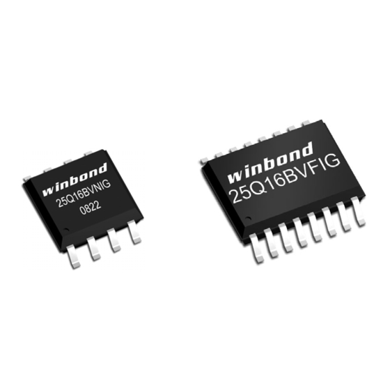
W25Q16BV Package Types W25Q16BV is offered in an 8-pin plastic 150-mil or 208-mil width SOIC (package code SN & SS) and 6x5-mm WSON (package code ZP) as shown in figure 1a, and 1b, respectively. The 300-mil 8-pin PDIP is another option of package selections (Figure 1c). The W25Q16BV is also offered in a 16-pin plastic 300-mil width SOIC (package code SF) as shown in figure 1d. -
Page 7: Block Diagram
Column Decode And 256-Byte Page Buffer And 256-Byte Page Buffer Data Data DI (IO DI (IO DO (IO DO (IO Byte Address Byte Address Latch / Counter Latch / Counter Figure 2. W25Q16BV Serial Flash Memory Block Diagram - 10 -... -
Page 8: Functional Description
10.1.4 Hold Function The /HOLD signal allows the W25Q16BV operation to be paused while it is actively selected (when /CS is low). The /HOLD function may be useful in cases where the SPI data and clock signals are shared with other devices. -
Page 9: Write Protection
One Time Program (OTP) write protection Note 1: These features are available upon special order. Please refer to Ordering Information. Upon power-up or at power-down, the W25Q16BV will maintain a reset condition while VCC is below the threshold value of V , (See Power-up Timing and Voltage Levels and Figure 32). -
Page 10: Control And Status Registers
W25Q16BV CONTROL AND STATUS REGISTERS The Read Status Register-1 and Status Register-2 instructions can be used to provide status on the availability of the Flash memory array, if the device is write enabled or disabled, the state of write protection, the Quad SPI setting and Erase Suspend status. The Write Status Register instruction can be used to configure the devices write protection features and Quad SPI setting. - Page 11 W25Q16BV 11.1.6 Status Register Protect (SRP1, SRP0) The Status Register Protect bits (SRP1 and SRP0) are non-volatile read/write bits in the status register (S8 and S7). The SRP bits control the method of write protection: software protection, hardware protection, power supply lock-down or one time programmable (OTP) protection.
- Page 12 W25Q16BV SRP0 SRP0 WEL BUSY WEL BUSY STATUS REGISTER PROTECT 0 STATUS REGISTER PROTECT 0 (non-volatile) (non-volatile) SECTOR PROTECT SECTOR PROTECT (non-volatile) (non-volatile) TOP/BOTTOM PROTECT TOP/BOTTOM PROTECT (non-volatile) (non-volatile) BLOCK PROTECT BITS BLOCK PROTECT BITS (non-volatile) (non-volatile) WRITE ENABLE LATCH...
- Page 13 W25Q16BV 1 1.1.9 Status Register Memory Protection STATUS REGISTER W25Q16BV (16M-BIT) MEMORY PROTECTION BLOCK(S) ADDRESSES DENSITY PORTION NONE NONE NONE NONE 1F0000h – 1FFFFFh 64KB Upper 1/32 30 and 31 1E0000h – 1FFFFFh 128KB Upper 1/16 28 thru 31 1C0000h – 1FFFFFh...
- Page 14 W25Q16BV 11.2 INSTRUCTIONS The instruction set of the W25Q16BV consists of thirty basic instructions that are fully controlled through the SPI bus (see Instruction Set table1-3). Instructions are initiated with the falling edge of Chip Select (/CS). The first byte of data clocked into the DI input provides the instruction code. Data on the DI input is sampled on the rising edge of clock with most significant bit (MSB) first.
-
Page 15: Instruction Set Table 1 (Erase, Program Instructions)
W25Q16BV 11.2.2 Instruction Set Table 1 (Erase, Program Instructions) BYTE 1 INSTRUCTION NAME BYTE 2 BYTE 3 BYTE 4 BYTE 5 BYTE 6 (CODE) Write Enable Write Disable Read Status Register-1 (S7–S0) Read Status Register-2 (S15-S8) Write Status Register (S7–S0) -
Page 16: Instruction Set Table 2 (Read Instructions)
W25Q16BV 11.2.3 Instruction Set Table 2 (Read Instructions) BYTE 1 INSTRUCTION NAME BYTE 2 BYTE 3 BYTE 4 BYTE 5 BYTE 6 (CODE) Read Data A23-A16 A15-A8 A7-A0 (D7-D0) Fast Read A23-A16 A15-A8 A7-A0 dummy (D7-D0) Fast Read Dual Output... -
Page 17: Instruction Set Table 3 (Id, Security Instructions)
W25Q16BV 11.2.4 Instruction Set Table 3 (ID, Security Instructions) INSTRUCTION BYTE 1 BYTE 2 BYTE 3 BYTE 4 BYTE 5 BYTE 6 NAME (CODE) Release Power down / dummy dummy dummy (ID7-ID0) Device ID Manufacturer/ dummy dummy (MF7-MF0) (ID7-ID0) Device ID... -
Page 18: Write Enable (06H)
W25Q16BV 11.2.5 Write Enable (06h) The Write Enable instruction (Figure 4) sets the Write Enable Latch (WEL) bit in the Status Register to a 1. The WEL bit must be set prior to every Page Program, Sector Erase, Block Erase, Chip Erase and Write Status Register instruction. -
Page 19: Read Status Register-1 (05H) And Read Status Register-2 (35H)
W25Q16BV 11.2.7 Read Status Register-1 (05h) and Read Status Register-2 (35h) The Read Status Register instructions allow the 8-bit Status Registers to be read. The instruction is entered by driving /CS low and shifting the instruction code “05h” for Status Register-1 and “35h” for Status Register-2 into the DI pin on the rising edge of CLK. - Page 20 W25Q16BV 11.2.8 Write Status Register (01h) The Write Status Register instruction allows the Status Register to be written. A Write Enable instruction must previously have been executed for the device to accept the Write Status Register Instruction (Status Register bit WEL must equal 1). Once write enabled, the instruction is entered by driving /CS low, sending the instruction code “01h”, and then writing the status register data byte as illustrated in figure 7.
- Page 21 W25Q16BV 11.2.9 Read Data (03h) The Read Data instruction allows one more data bytes to be sequentially read from the memory. The instruction is initiated by driving the /CS pin low and then shifting the instruction code “03h” followed by a 24-bit address (A23-A0) into the DI pin.
-
Page 22: Fast Read (0Bh)
W25Q16BV 11.2.10 Fast Read (0Bh) The Fast Read instruction is similar to the Read Data instruction except that it can operate at the highest possible frequency of F (see AC Electrical Characteristics). This is accomplished by adding eight “dummy” clocks after the 24-bit address as shown in figure 9. The dummy clocks allow the devices internal circuits additional time for setting up the initial address. - Page 23 IO and IO . This allows data to be transferred from the W25Q16BV at twice the rate of standard SPI devices. The Fast Read Dual Output instruction is ideal for quickly downloading code from Flash to RAM upon power-up or for applications that cache code-segments to RAM for execution.
-
Page 24: Fast Read Quad Output (6Bh)
Fast Read Quad Output Instruction (Status Register bit QE must equal 1). The Fast Read Quad Output Instruction allows data to be transferred from the W25Q16BV at four times the rate of standard SPI devices. - Page 25 W25Q16BV 11.2.13 Fast Read Dual I/O (BBh) The Fast Read Dual I/O (BBh) instruction allows for improved random access while maintaining two IO pins, IO and IO . It is similar to the Fast Read Dual Output (3Bh) instruction but with the capability to input the Address bits (A23-0) two bits per clock.
- Page 26 W25Q16BV Figure 12b. Fast Read Dual I/O Instruction Sequence Diagram (M7-0 = Axh) Publication Release Date: July 08, 2010 - 29 - Revision F...
- Page 27 W25Q16BV 11.2.14 Fast Read Quad I/O (EBh) The Fast Read Quad I/O (EBh) instruction is similar to the Fast Read Dual I/O (BBh) instruction except that address and data bits are input and output through four pins IO , IO...
- Page 28 W25Q16BV Figure 13b. Fast Read Quad I/O Instruction Sequence Diagram (M7-0 = Axh) Publication Release Date: July 08, 2010 - 31 - Revision F...
-
Page 29: Word Read Quad I/O (E7H)
W25Q16BV 11.2.15 Word Read Quad I/O (E7h) The Word Read Quad I/O (E7h) instruction is similar to the Fast Read Quad I/O (EBh) instruction except that the lowest Address bit (A0) must equal 0 and only two Dummy clocks are required prior to the data output. - Page 30 W25Q16BV Byte 1 Byte 1 Byte 2 Byte 2 Byte 3 Byte 3 Figure 14b. Word Read Quad I/O Instruction Sequence Diagram (M7-0 = Axh) Publication Release Date: July 08, 2010 - 33 - Revision F...
-
Page 31: Octal Word Read Quad I/O (E3H)
W25Q16BV 11.2.16 Octal Word Read Quad I/O (E3h) The Octal Word Read Quad I/O (E3h) instruction is similar to the Fast Read Quad I/O (EBh) instruction except that the lower four Address bits (A0, A1, A2, A3) must equal 0. As a result, the four dummy clocks are not required, which further reduces the instruction overhead allowing even faster random access for code execution (XIP). - Page 32 W25Q16BV Byte 1 Byte 1 Byte 2 Byte 2 Byte 3 Byte 3 Byte 4 Byte 4 Figure 15b. Octal Word Read Quad I/O Instruction Sequence Diagram (M7-0 = Axh) Publication Release Date: July 08, 2010 - 35 - Revision F...
-
Page 33: Page Program (02H)
W25Q16BV 11.2.17 Page Program (02h) The Page Program instruction allows from one byte to 256 bytes (a page) of data to be programmed at previously erased (FFh) memory locations. A Write Enable instruction must be executed before the device will accept the Page Program Instruction (Status Register bit WEL= 1). The instruction is initiated by driving the /CS pin low then shifting the instruction code “02h”... - Page 34 W25Q16BV 11.2.18 Quad Input Page Program (32h) The Quad Page Program instruction allows up to 256 bytes of data to be programmed at previously erased (FFh) memory locations using four pins: IO , IO , IO , and IO . The Quad Page Program can improve performance for PROM Programmer and applications that have slow clock speeds <5MHz.
-
Page 35: Sector Erase (20H)
W25Q16BV 11.2.19 Sector Erase (20h) The Sector Erase instruction sets all memory within a specified sector (4K-bytes) to the erased state of all 1s (FFh). A Write Enable instruction must be executed before the device will accept the Sector Erase Instruction (Status Register bit WEL must equal 1). -
Page 36: 32Kb Block Erase (52H)
W25Q16BV 11.2.20 32KB Block Erase (52h) The Block Erase instruction sets all memory within a specified block (32K-bytes) to the erased state of all 1s (FFh). A Write Enable instruction must be executed before the device will accept the Block Erase Instruction (Status Register bit WEL must equal 1). -
Page 37: 64Kb Block Erase (D8H)
W25Q16BV 11.2.21 64KB Block Erase (D8h) The Block Erase instruction sets all memory within a specified block (64K-bytes) to the erased state of all 1s (FFh). A Write Enable instruction must be executed before the device will accept the Block Erase Instruction (Status Register bit WEL must equal 1). - Page 38 W25Q16BV 11.2.22 Chip Erase (C7h / 60h) The Chip Erase instruction sets all memory within the device to the erased state of all 1s (FFh). A Write Enable instruction must be executed before the device will accept the Chip Erase Instruction (Status Register bit WEL must equal 1).
- Page 39 W25Q16BV 11.2.23 Erase Suspend (75h) The Erase Suspend instruction “75h”, allows the system to interrupt a Sector or Block Erase operation and then read from or program data to, any other sectors or blocks. The Erase Suspend instruction sequence is shown in figure 22.
- Page 40 W25Q16BV 11.2.24 Erase Resume (7Ah) The Erase Resume instruction “7Ah” must be written to resume the Sector or Block Erase operation after an Erase Suspend. The Resume instruction “7Ah” will be accepted by the device only if the SUS bit in the Status Register equals to 1 and the BUSY bit equals to 0.
- Page 41 W25Q16BV 11.2.25 Power-down (B9h) Although the standby current during normal operation is relatively low, standby current can be further reduced with the Power-down instruction. The lower power consumption makes the Power-down instruction especially useful for battery powered applications (See ICC1 and ICC2 in AC Characteristics).
- Page 42 CLK with most significant bit (MSB) first as shown in figure 25b. The Device ID values for the W25Q16BV is listed in Manufacturer and Device Identification table. The Device ID can be read continuously. The instruction is completed by driving /CS high.
- Page 43 W25Q16BV Figure 25b. Release Power-down / Device ID Instruction Sequence Diagram - 46 -...
-
Page 44: Read Manufacturer / Device Id (90H)
Device ID are shifted out on the falling edge of CLK with most significant bit (MSB) first as shown in figure 26. The Device ID values for the W25Q16BV is listed in Manufacturer and Device Identification table. If the 24-bit address is initially set to 000001h the Device ID will be read first and then followed by the Manufacturer ID. -
Page 45: Read Manufacturer / Device Id Dual I/O (92H)
24-bit address (A23-A0) of 000000h, 8-bit Continuous Read Mode Bits, with the capability to input the Address bits two bits per clock. After which, the Manufacturer ID for Winbond (EFh) and the Device ID are shifted out 2 bits per clock on the falling edge of CLK with most significant bits (MSB) first as shown in figure 27. - Page 46 Address bits four bits per clock. After which, the Manufacturer ID for Winbond (EFh) and the Device ID are shifted out four bits per clock on the falling edge of CLK with most significant bit (MSB) first as shown in figure 28.
-
Page 47: Read Unique Id Number (4Bh)
The Read Unique ID Number instruction accesses a factory-set read-only 64-bit number that is unique to each W25Q16BV device. The ID number can be used in conjunction with user software methods to help prevent copying or cloning of a system. The Read Unique ID instruction is initiated by driving the /CS pin low and shifting the instruction code “4Bh”... - Page 48 2003. The instruction is initiated by driving the /CS pin low and shifting the instruction code “9Fh”. The JEDEC assigned Manufacturer ID byte for Winbond (EFh) and two Device ID bytes, Memory Type (ID15-ID8) and Capacity (ID7-ID0) are then shifted out on the falling edge of CLK with most significant bit (MSB) first as shown in figure 30.
-
Page 49: Continuous Read Mode Reset (Ffh Or Ffffh)
If the system controller is Reset during operation it will likely send a standard SPI instruction, such as Read ID (9Fh) or Fast Read (0Bh), to the W25Q16BV. However, as with most SPI Serial Flash memories, the W25Q16BV does not have a hardware Reset pin, so if Continuous Read Mode bits are set to “Ax”... -
Page 50: Electrical Characteristics
W25Q16BV 12. ELECTRICAL CHARACTERISTICS 12.1 Absolute Maximum Ratings PARAMETERS SYMBOL CONDITIONS RANGE UNIT Supply Voltage –0.6 to +4.0 Voltage Applied to Any Pin Relative to Ground –0.6 to VCC+0.4 <20nS Transient Transient Voltage on any Pin –2.0V to VCC+2.0V Relative to Ground Storage Temperature –65 to +150... -
Page 51: Power-Up Timing And Write Inhibit Threshold
W25Q16BV 12.3 Power-up Timing and Write Inhibit Threshold SPEC PARAMETER SYMBOL UNIT VCC (min) to /CS Low µs Time Delay Before Write Instruction Write Inhibit Threshold Voltage Note: 1. These parameters are characterized only. Figure 32. Power-up Timing and Voltage Levels... -
Page 52: Dc Electrical Characteristics
W25Q16BV 12.4 DC Electrical Characteristics SPEC PARAMETER SYMBOL CONDITIONS UNIT IN (1) Input Capacitance = 0V Output Capacitance Cout = 0V ±2 µA Input Leakage I/O Leakage ±2 µA /CS = VCC, Standby Current µA VIN = GND or VCC... -
Page 53: Ac Measurement Conditions
W25Q16BV 12.5 AC Measurement Conditions SPEC PARAMETER SYMBOL UNIT Load Capacitance Input Rise and Fall Times Input Pulse Voltages 0.2 VCC to 0.8 VCC Input Timing Reference Voltages 0.3 VCC to 0.7 VCC Output Timing Reference Voltages 0.5 VCC to 0.5 VCC Note: 1. -
Page 54: Ac Electrical Characteristics
W25Q16BV 12.6 AC Electrical Characteristics SPEC DESCRIPTION SYMBOL UNIT Clock frequency for all instructions, except Read Data (03h) & Octal Word Read (E3h) D.C. 2.7V-3.6V VCC & Industrial Temperature Clock frequency for all instructions, except Read Data (03h) & Octal Word Read (E3h) D.C. - Page 55 W25Q16BV 12.7 AC Electrical Characteristics ( cont’d) SPEC DESCRIPTION SYMBOL UNIT /HOLD Active Setup Time relative to CLK HLCH /HOLD Active Hold Time relative to CLK CHHH /HOLD Not Active Setup Time relative to CLK HHCH /HOLD Not Active Hold Time relative to CLK...
- Page 56 W25Q16BV 12.8 Serial Output Timing 12.9 Serial Input Timing 12.10 Hold Timing Publication Release Date: July 08, 2010 - 59 - Revision F...
-
Page 57: 8-Pin Soic 150-Mil (Package Code Sn)
W25Q16BV PACKAGE SPECIFICATION 13.1 8-Pin SOIC 150-mil (Package Code SN) θ θ 0.25 0.25 SEATING PLANE SEATING PLANE GAUGE PLANE GAUGE PLANE b b b MILLIMETERS INCHES SYMBOL 1.35 1.75 0.053 0.069 0.10 0.25 0.004 0.010 0.33 0.51 0.013 0.020 0.19... -
Page 58: 8-Pin Soic 208-Mil (Package Code Ss)
W25Q16BV 13.2 8-Pin SOIC 208-mil (Package Code SS) GAUGE PLANE GAUGE PLANE MILLIMETERS INCHES SYMBOL 1.75 1.95 2.16 0.069 0.077 0.085 0.05 0.15 0.25 0.002 0.006 0.010 1.70 1.80 1.91 0.067 0.071 0.075 0.35 0.42 0.48 0.014 0.017 0.019 0.19 0.20... -
Page 59: 8-Pin Pdip 300-Mil (Package Code Da)
W25Q16BV 13.3 8-Pin PDIP 300-mil (Package Code DA) MILLIMETERS INCHES SYMBO 5.33 0.210 0.38 0.015 3.18 3.30 3.43 0.125 0.130 0.135 9.02 9.27 10.16 0.355 0.365 0.400 7.62 BSC. 0.300 BSC. 6.22 6.35 6.48 0.245 0.250 0.255 2.92 3.30 3.81 0.115... - Page 60 W25Q16BV 13.4 8-Contact 6x5mm WSON (Package Code ZP) MILLIMETERS INCHES SYMBOL 0.70 0.75 0.80 0.028 0.030 0.031 0.00 0.02 0.05 0.000 0.001 0.002 0.35 0.40 0.48 0.014 0.016 0.019 0.20 REF. 0.008 REF. 5.90 6.00 6.10 0.232 0.236 0.240 3.35 3.40...
- Page 61 0.026 Notes: 1. Advanced Packaging Information; please contact Winbond for the latest minimum and maximum specifications. 2. BSC = Basic lead spacing between centers. 3. Dimensions D and E do not include mold flash protrusions and should be measured from the bottom of the package.
- Page 62 W25Q16BV 13.5 16-Pin SOIC 300-mil (Package Code SF) GAUGE PLANE GAUGE PLANE DETAIL A DETAIL A MILLIMETERS INCHES SYMBOL 2.36 2.49 2.64 0.093 0.098 0.104 0.10 0.30 0.004 0.012 2.31 0.091 0.33 0.41 0.51 0.013 0.016 0.020 0.18 0.23 0.28 0.007...
-
Page 63: Ordering Information
W25Q16BV ORDERING INFORMATION W 25Q 16B V xx W = Winbond 25Q = SpiFlash Serial Flash Memory with 4KB sectors, Dual/Quad I/O 16B = 16M-bit V = 2.7V to 3.6V SN = 8-pin SOIC 150-mil ZP = 8-pad WSON 6x5mm... - Page 64 W25Q16BV 14.1 Valid Part Numbers and Top Side Marking The following table provides the valid part numbers for the W25Q16BV SpiFlash Memory. Please contact Winbond for specific availability by density and package type. Winbond SpiFlash memories use an 12- digit Product Number for ordering. However, due to limited space, the Top Side Marking on all packages use an abbreviated 10-digit number.
Need help?
Do you have a question about the W25Q16BV and is the answer not in the manual?
Questions and answers