Table of Contents
Advertisement
Quick Links
SERVICE MANUAL
Ver 1.0 2000. 08
General
Spread method
Direct-Sequence Spread-Spectrum
Access method
FDMA-TDD
Operation frequency
902 - 928 MHz
Operating channel
14 channels
Dial signal
Tone, 10 PPS (pulse) selectable
Handset
Power source
Rechargeable battery pack BP-T31
Battery charging time
Approx. 12 hours
Battery life
Standby: Approx. 7 days
Talk:
Dimensions
Approx. 2
antenna excluded
(approx. 56 x 183 x 55 mm)
Antenna: Approx. 3 inches
(approx. 75 mm)
Mass
Approx. 9.5 oz (approx. 270 g), battery
included
SPECIFICATIONS
Approx. 6 hours
1
1
1
⁄
x 7
⁄
x 2
⁄
inches (w/h/d),
4
4
4
SPP-A9171
Base unit
Power source
DC 9V from AC power adaptor AC-T46
Battery charging time
Approx. 24 hours
Dimensions
3
7
3
Approx. 6
⁄
x 2
⁄
x 8
⁄
8
8
4
antenna excluded
(approx. 160 x 71 x 222 mm)
1
Antenna: Approx. 4
⁄
inches
2
(approx. 113 mm)
Mass
Approx. 1 lb 3 oz (approx. 540 g), wall
bracket excluded
Answering machine
Maximum recording time
About 18 minutes (at NORM (Long)
recording quality), using incorporated IC
Greeting message
Up to 4 minutes
Incoming message
Up to 4 minutes/message
Memo
Up to 4 minutes/message
Design and specifications are subject to
change without notice.
CORDLESS TELEPHONE
US Model
Canadian Model
inches (w/h/d),
Advertisement
Chapters
Table of Contents

Related Manuals for Sony SPP-A9171


Summary of Contents for Sony SPP-A9171
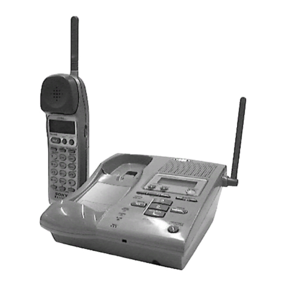
- Page 1 SPP-A9171 SERVICE MANUAL US Model Canadian Model Ver 1.0 2000. 08 SPECIFICATIONS General Base unit Spread method Power source Direct-Sequence Spread-Spectrum DC 9V from AC power adaptor AC-T46 Access method Battery charging time FDMA-TDD Approx. 24 hours Operation frequency Dimensions 902 - 928 MHz Approx.
-
Page 2: Table Of Contents
PIÈCES SONT CRITIQUES POUR LA SÉCURITÉ DE FONCTIONNEMENT. NE REMPLACER CES COMPOSANTS 6. DIAGRAMS QUE PAR DES PIÈCES SONY DONT LES NUMÉROS 6-1. IC Block Diagrams ............34 6-2. Block Diagram –Base Unit (Main) Section– ....35 SONT DONNÉS DANS CE MANUEL OU DANS LES –Handset Section–... -
Page 3: General
Before you use your phone, you must set it up. Here’s a quick way to set up your phone: Steps 1, 2, 3 and 4. Make sure you have received the following items in the package. If anything is missing, contact your local Sony dealer. Step 1 (page 7) First, unpack the phone and the supplied accessories. - Page 4 If the battery lasts only a few minutes even after 12 hours of charging, the usable life of the battery has expired and needs replacement. Contact your local Sony authorized dealer or service center, and ask for Sony BP-T31 rechargeable battery pack.
- Page 5 Step 4 Entering the area code Notes • If the home area code is already entered, it appears on the display in step 3. To enter a different home area code, see “To change the home area code” below. When you use this phone for the first time, or move to an area •...
-
Page 6: Identifying The Parts
Identifying the parts Display Refer to the pages indicated in parentheses for details. The display on the base unit shows the Base Unit answering machine operation. wdwf wgwhwj ql HANDSET LOCATOR button 1 Memory capacity indicator 1 ERASE button (p. 37, 45) 9 CHARGE lamp (p. -
Page 7: Making Calls
Basics Making calls Notes • When you increase the sound volume, in some cases the background noise may be increased as well. You should adjust the volume accordingly. Pick up the handset from the • If the handset beeps every second during conversation and “OUT OF base unit. -
Page 8: Phone Directory
Storing phone numbers and names Enter the phone number. SONY You can enter up to 20 digits, including a tone 1234567 Example: to store “SONY” “123-4567”. and a pause, each of which is counted as one Turn Press digit. Press (PGM). -
Page 9: Preparing The Answering Machine
Turn Jog Dial up to make “YES” flash, then press Jog Dial. • Initial character: To search for “SONY” for example, press (7) and You hear a long confirmation beep and the then turn Jog Dial to search through the names starting with P, Q, R, S or 7. -
Page 10: Recording The Greeting
Preparing the answering machine (continued) Recording the greeting This answering machine has prerecorded greetings (see page 37). Set the hour (1 to 12) and choose “AM” or SET DAY & TIME However, you can record your own greeting. “PM” by turning Jog Dial, and then press Jog SUNDAY The greeting must be between two seconds and four minutes long. -
Page 11: Selecting The Ring Time
Preparing the answering machine (continued) Selecting the recording quality Selecting the ring time For the user who does not utilize the maximum recording capacity (about 18 minutes), you can select a higher recording grade and enjoy You can select the number of rings before the answering machine superior sound quality and clarity compared to the standard (NORM) starts to play back the greeting and records incoming messages. -
Page 12: Playing Back Messages
Preparing the answering machine (continued) Playing back messages (MAILBOX 1) Display Mailbox usage When you come home (MAILBOX 2) (ERASE) This phone offers you three voice mailboxes, providing a convenient (MAILBOX 3) If (ANSWER ON/OFF) flashes in way to share the mailbox feature with other members of your red, or the message counter household or business. -
Page 13: Screening Incoming Calls
Screening incoming calls Recording a memo You can screen calls by leaving the answering function on (see page You can record a “memo” (up to four minutes) as a personal reminder 41) while you are at home. When a call is answered, you can hear the or as a message for other people. -
Page 14: Looking At The Caller Id List
Caller ID Features Operating from an outside phone (continued) Understanding the Caller ID service Caller ID allows the caller’s phone number to be shown on the display Picking up new messages before you answer the call. In order to use this feature, you must first Call your phone from a touch-tone phone. -
Page 15: Using The Caller Id List
Using the Caller ID list Looking at the Caller ID list (continued) By using the Caller ID list, you can call back a phone number from the To erase the entire list at once Caller ID list easily, or store numbers from the Caller ID list into the Phone Directory. -
Page 16: Mounting The Base Unit On A Wall
Using the Caller ID list (continued) Using “Caller ID with call waiting” service When the local area code matches This telephone is compatible with the “Caller ID with call waiting” SMITH JOHN SMITH JOHN service. Make sure that your telephone company offers this service. 1-123-4567 201-123-4567 Like the basic Caller ID service, you need to subscribe to “Caller ID... -
Page 17: Disassembly
SECTION 2 DISASSEMBLY Note: Follow the disassembly procedure in the numerical order given. 2-1. CABINET (REAR)(HANDSET) 2-2. HAND MAIN BOARD (HANDSET) Nickel cadmium battery Screw (BTP 2.6x12) Screw (BTP 2.6x8) Two screws (BTP 2.6x8) Two screws (BTP 2.6x12) Cabinet (rear) Battery case lid Connector (CN601) Hand main board... -
Page 18: Mhz System Operation
SECTION 3 900 MHz SYSTEM OPERATION 3-1. ACCESS METHOD 3-2. PROTOCOL 1. Transfer Format & Rate 1. General The transfer format & rate of our system is as follows; This system realizes the TX/RX superframe by TDD system. The relation of master/slave dose not decide identification regarding the Table 3-1. - Page 19 4. Stand-by Mode Operation (1) HANDSET When the HANDSET is the stand-by mode (sleep mode), the HANDSET do the intermittent operation for power save, because the HANDSET is the battery operation. This process of stand-by mode operation is as follows. 10 sec 10 sec Heart-Beat...
- Page 20 5. Link Establishment Master Slave According to the following Fig. 3-1, the requested side for link establishment is the master. The system have to exchange the A-Frame for link establishment, and each system ID should be the same ID, and then the system link A-Frame is established.
-
Page 21: Test Mode
SECTION 4 TEST MODE 4-1. BASE UNIT TEST MODE A [Base Set AUDIO Input/Output Level test [ADPCM Forward Loop Back (L2) Mode]] Manual System Test Mode Level meter [Start-up] Audio analyzer 1. Set the DIAL MODE switch to P (PULSE), and turn on the power while pressing the MEMO ANSWER BOX3 key. -
Page 22: Base Unit Test Mode B
4-2. BASE UNIT TEST MODE B HANDSET LOCATOR Manual System Test Mode Radio mode button pressing [Start-up] count 1. Set the DIAL MODE switch to T (TONE), and turn on the 1ch single carrier continuous transmission mode power while pressing the MEMO ANSWER BOX3 key. (high power) 2. -
Page 23: Base Unit Test Mode
4-3. BASE UNIT TEST MODE 3. LCD Test; LCD “2” indication Select the test mode “2” from the test mode idle state using the VOLUME +/- keys. Press the “ANSWER” key and the system Automatic Answering System Test Mode enters the test mode “2” [LCD test mode]. •... - Page 24 5. Caller-ID Detection Test; LCD”4” indication (4) LINE playback audio path setting Select the test mode “4” from the test mode idle state using the The LINE playback audio path can be set by pressing the VOLUME +/- keys. Press the “ANSWER” key and the system “REPEAT”...
-
Page 25: Handset Test Mode
4-4. HANDSET TEST MODE 9. RECORDING QUALITY Slide Switch Test; LCD ”8” indication Select the test mode “8” from the test mode idle state using the [Start-Up] VOLUME +/- keys. Press the “ANSWER” key and the system 1. Press the TALK , 0 , and 1 keys simultaneously to start. enters the test mode “8”... - Page 26 C) Continuous Transmission Test D) Loopback Test Command Mode/Operation Mode/Operation Command 2-1-# One channel continuous send (TX power: HIGH) 3-1-# CODEC Forward Loopback (L1) 2-2-# One channel continuous send (TX power: Medium) (MIC n SP) (within CODEC) 2-3-# One channel continuous send (TX power: Low) 3-2-# ADPCM Forward Loopback (L2) 2-4-#...
- Page 27 Details 4-5. RF TESTING 1. Key Matrix Test: 5-1-# This test is for checking the RF system without disassembling the If the keys are pressed continuously in the following desig nated set in servicing. Perform measurement using the spectrum analyzer order correctly, a confirmation beep sounds.
- Page 28 • Transmission Wave: –16.00 dBm ATTEN 10 dB 0 dBm 10 dB/ 903.392 MHz –5 –6 –1 –4 –7 903.392 MHz 18dB –3 –16.00 dBm –2 –8 –9 CENTER 904.2 MHz SPAN 5.000 MHz Fig. 4 50.0 msec 30 kHz 30 kHz Fig.
- Page 29 • Measurement: Measure peak level by Spectrum analyzer. 903.587 MHz .0 dBm AT 10 dB –3.67 dBm PEAK PLOTTER ADRS WA SB SC FC CORR CENTER 903.600 MHz SPAN 5.000 MHz RES BW 1.0 MHz VBW 100 kHz SWP 20.0 msec •...
-
Page 30: Electrical Adjustments
SECTION 5 ELECTRICAL ADJUSTMENTS 5-1. BASE UNIT SECTION 3. Checking TX Output Setting: • Make the set in Test mode (see page 21) peak power meter 1. Checking RX I&Q Output Level Setting: ANTENNA TERMINAL – oscilloscope level meter TP558: RXIP Procedure: TP557: RXIN 1. -
Page 31: Handset Section
5-2. HANDSET SECTION 3. Checking TX Output Setting: • Make the set in Test mode (see page 21) peak power meter 1. Checking RX I&Q Output Level Setting: ANTENNA TERMINAL (TP812) – oscilloscope level meter TP804: RXIP Procedure: TP803: RXIN 1. - Page 32 ADJUSTMENT LOCATION: [BASE MAIN BOARD] (Conductor Side) TP555 : RXQN TP556 : RXQP TP557 : RXIN TP558 : RXIP level meter Chcking RX I & Q Output Level ANTENNA TERMINAL short : TP515 ˜ TP567 (GND) : Checking RX I & Q Output Level Checking TX Center Frequency frequency counter : Checking TX Center Frequency peak power meter : Checking TX Output...
-
Page 33: Diagrams
SECTION 6 DIAGRAMS Waveforms THIS NOTE IS COMMON FOR PRINTED WIRING – BASE UNIT SECTION – BOARDS AND SCHEMATIC DIAGRAMS. (In addition to this, the necessary note is printed in each block.) For schematic diagrams. 4 Vp-p Note: • All capacitors are in µF unless otherwise noted. pF: µµF 9.6 MHz 50 WV or less are not indicated except for electrolytics and tantalums. -
Page 34: Ic Block Diagrams
6-1. IC BLOCK DIAGRAMS • BASE MAIN Board • HAND MAIN Board IC502 S-24C01AFJA-TB-01 IC402 AT24C32N-10SI-1.8-TR DOUT START/ STOP LOGIC LOGIC H.V. DOUT/ACK SERIAL PUMP/ LOAD DEVICE CONTROL TIMING COMP ADDRESS LOGIC TEST COMPARATOR SERIAL MUX Y DEC DATA EEPROM ADDRESS/COUNTER RECOVERY DATA WORD... -
Page 35: Block Diagram -Base Unit (Main) Section
SPP-A9171 6-2. BLOCK DIAGRAM –BASE UNIT SECTION– RFU801 IC501 IC351 ANT701 RF UNIT ASIC DSP/CODEC (ANTENNA) SP901 RXIP RXIP (SPEAKER) CIDIP RXIN RXIN CIDIN RXQP RXQP SPOUTP RAQN RAQN SPOUTN RXEN RXEN MJ101 TXDATA D111-114 TXDATA TXEN TXEN LNAATTN LNAATN... -
Page 36: Handset Section
SPP-A9171 –HANDSET SECTION– RFU801 IC401 RF UNIT ANT1 ASIC (ANTENNA) SP601 (SPEAKER) : TX RXIP RXIP RXIN RXIN SPKROP : RX RXQP RXQP RAQN SPKRON RAQN : BELL RXEN RXEN TXDATA TXDATA MIC601 TXEN TXEN LNAATTN LNATTN (MIC) MICINP TXPWR0... -
Page 37: Printed Wiring Board -Base Main Section
SPP-A9171 6-3. PRINTED WIRING BOARD –BASE MAIN SECTION– • See page 33 for Note on Printed Wiring Board and Semiconductor Location. D103 D102 D104 D105 BASE KEY BOARD (Page 46) BASE KEY BOARD (Page 46) DSP BOARD (Page 51) — 39 —... - Page 38 SPP-A9171 • See page 33 for Note on Schematic Diagrams. 6-4. SCHEMATIC DIAGRAM –BASE MAIN SECTION (1/2)– — 41 — — 42 —...
- Page 39 SPP-A9171 6-5. SCHEMATIC DIAGRAM –BASE MAIN SECTION (2/2)– • See page 33 for Note on Schematic Diagrams. — 43 — — 44 —...
-
Page 40: Printed Wiring Board -Base Key Section
SPP-A9171 • See page 33 for Note on Printed Wiring Board. 6-6. PRINTED WIRING BOARD –BASE KEY SECTION– • Semiconductor Location Ref. No. Location D301 D302 D303 D304 D305 D306 D307 D308 D309 D310 D311 D312 D313 (Page 39) D314... -
Page 41: Schematic Diagram -Base Key Section
SPP-A9171 6-7. SCHEMATIC DIAGRAM –BASE KEY SECTION– • See page 33 for Note on Schematic Diagrams. — 47 — — 48 —... -
Page 42: Printed Wiring Board -Display Section
SPP-A9171 • See page 33 for Note on Printed Wiring Board. 6-8. PRINTED WIRING BOARD –DISPLAY SECTION– (Page 40) C385 1-678-526 1-678-526 — 49 — — 50 —... -
Page 43: Schematic Diagram -Disp Section
SPP-A9171 6-9. SCHEMATIC DIAGRAM –DISPLAY SECTION– • See page 33 for Note on Schematic Diagrams. — 51 — — 52 —... -
Page 44: Printed Wiring Board -Hand Main Section
SPP-A9171 • See page 33 for Note on Printed Wiring Board. 6-10. PRINTED WIRING BOARD –HAND MAIN SECTION– • Semiconductor Location Ref. No. Location D201 D202 D203 D205 D206 D207 D208 D209 D401 D404 D405 D406 D407 D408 D409 D410... -
Page 45: Schematic Diagram -Hand Main Section
SPP-A9171 6-11. SCHEMATIC DIAGRAM –HAND MAIN SECTION– • See page 33 for Note on Schematic Diagrams. — 55 — — 56 —... -
Page 46: Ic Pin Functions
SPP-A9171 6-12. IC PIN FUNCTIONS • BASE MAIN BOARD IC501 R6797-76 (HUMMINGBIRD ASIC) Pin No. Pin Name Function Pin No. Pin Name Function VSSC – VSS supply to core CDCICLK – Bit clock input/output for digital serial interface Not used (open) VDDP –... - Page 47 • HAND MAIN BOARD IC401 R6797-76 (HUMMINGBIRD ASIC) Pin No. Pin Name Function VSSC – VSS supply to core VDDP – VDD supply to pad ring VSSP – VSS supply to pad ring OSCO 9.6 MHz crystal oscillator output OSCI 9.6 MHz crystal oscillator input RING ON/OFF Detection signal input of the ringer coming...
- Page 48 Pin No. Pin Name Function Bit clock input/output for digital serial interface Not used (open) CDCICLK Codec reset RESETOP Keypad bidirectional control/LCD data KEYPADC0 – Keypad bidirectional control/LCD data KEYPADC1 – Keypad bidirectional control/LCD data KEYPADC2 – Keypad bidirectional control/LCD data KEYPADC3 –...
- Page 49 • BASE MAIN BOARD IC201 TMP87CM21F (TAD CPU) Pin No. Pin Name Function – Ground XOUT Main clock output Main clock input RESET Reset signal input TADACK TADuC ACK output TADREQ TADuC REQ output TEST Test pin for out-going test STOP TADuC power down input ASICREQ...
-
Page 50: Exploded Views
SECTION 7 EXPLODED VIEWS NOTE: • -XX, -X mean standardized parts, so they may • The mechanical parts with no reference number The components identified by mark 0 or have some differences from the original one. in the exploded views are not supplied. dotted line with mark 0 are critical for safety. - Page 51 7-2. BASE MAIN SECTION SP901 LCD301 MIC1 Ref. No. Part No. Description Remarks Ref. No. Part No. Description Remarks 3-048-685-01 PANEL (LCD) X-3379-140-1 CABINET (LOWER) ASSY 3-034-829-01 LID(BASE), BATTERY CASE 3-037-081-01 PLUG(ANTENNA) X-3379-517-1 TERMINAL ASSY, CHARGE * 69 A-3622-469-A BASE MAIN BOARD, COMPLETE 3-048-688-01 LENS * 70 A-3673-094-A DSP BOARD, COMPLETE...
-
Page 52: Electrical Parts List
BASE KEY SECTION 8 ELECTRICAL PARTS LIST BASE MAIN NOTE: • Due to standardization, replacements in the • RESISTORS • Abbreviation parts list may be different from the parts All resistors are in ohms. CND : Canadian model. specified in the diagrams or the components METAL: metal-film resistor When indicating parts by reference number, used on the set. - Page 53 BASE MAIN Ref. No. Part No. Description Remarks Ref. No. Part No. Description Remarks C202 1-162-919-11 CERAMIC CHIP 22PF C903 1-126-154-11 ELECT 47uF 6.3V C203 1-162-117-00 CERAMIC 100PF 10.00% 500V C904 1-126-154-11 ELECT 47uF 6.3V C205 1-162-974-11 CERAMIC CHIP 0.01uF C905 1-162-921-11 CERAMIC CHIP 33PF...
-
Page 54: Q613
BASE MAIN Ref. No. Part No. Description Remarks Ref. No. Part No. Description Remarks < IC > Q613 8-729-120-28 TRANSISTOR 2SC1623-L5L6 Q614 8-729-922-34 TRANSISTOR 2SD1758F5-QR IC201 8-759-699-87 IC TMP87CM21F-IU09 Q615 8-729-026-49 TRANSISTOR 2SA1037AK-T146-R IC202 8-759-234-77 IC TC4S66F Q616 8-729-026-49 TRANSISTOR 2SA1037AK-T146-R IC501 8-759-699-16 IC R6797-76... - Page 55 BASE MAIN Ref. No. Part No. Description Remarks Ref. No. Part No. Description Remarks R221 1-216-821-11 METAL CHIP 1/16W R509 1-216-833-11 METAL CHIP 1/16W R222 1-216-821-11 METAL CHIP 1/16W R510 1-216-833-11 METAL CHIP 1/16W R223 1-216-821-11 METAL CHIP 1/16W R511 1-216-817-11 METAL CHIP 1/16W R224...
- Page 56 BASE MAIN Ref. No. Part No. Description Remarks Ref. No. Part No. Description Remarks R624 1-215-862-11 METAL OXIDE C376 1-162-921-11 CERAMIC CHIP 33PF R625 1-215-859-00 METAL OXIDE C377 1-162-921-11 CERAMIC CHIP 33PF R626 1-216-833-11 METAL CHIP 1/16W C378 1-162-921-11 CERAMIC CHIP 33PF R627 1-216-833-11 METAL CHIP...
- Page 57 HAND MAIN Ref. No. Part No. Description Remarks Ref. No. Part No. Description Remarks A-3673-091-A HAND MAIN BOARD, COMPLETE C620 1-162-921-11 CERAMIC CHIP 33PF C621 1-115-565-11 CERAMIC CHIP 2.2uF ************************** C622 1-162-921-11 CERAMIC CHIP 33PF 3-034-819-01 TERMINAL (H BATT), CHARGE C623 1-107-682-11 CERAMIC CHIP 3-038-844-01 SPACER (MICROPHONE CUSHION)
- Page 58 HAND MAIN Ref. No. Part No. Description Remarks Ref. No. Part No. Description Remarks L206 1-469-891-21 INDUCTOR R423 1-216-817-11 METAL CHIP 1/16W L207 1-469-891-21 INDUCTOR R424 1-216-845-11 METAL CHIP 100K 1/16W L401 1-414-733-11 INDUCTOR 100nH R425 1-216-845-11 METAL CHIP 100K 1/16W L402 1-414-528-11 INDUCTOR...
- Page 59 HAND MAIN MICROPHONE Ref. No. Part No. Description Remarks Ref. No. Part No. Description Remarks < MODULATOR > ACCESSORIES & PACKING MATERIALS ******************************* RFU801 1-476-251-11 RF UNIT 1-473-475-61 ADAPTOR, AC (AC-T46) < SWITCH > 1-528-976-11 BATTERY, NI-CD (BP-T31) 1-696-453-21 CORD (WITH MODULAR PLUG)(LINE) S401 1-762-636-11 SWITCH, SLIDE (RING) 1-696-454-11 CORD (WITH MODULAR PLUG)(LINE)
- Page 60 SPP-A9171 Sony Corporation 2000H16093-1 Audio Entertainment Group 9-927-982-11 Printed in Japan ©2000.8 — 72 — Published by General Engineering Dept.
Need help?
Do you have a question about the SPP-A9171 and is the answer not in the manual?
Questions and answers