Table of Contents
Advertisement
Quick Links
SERVICE MANUAL
SERVICE MANUAL
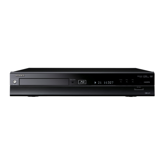
BLU-RAY DISC PLAYER
DBS-6.9
MODEL
Black model
BCDD
120V AC, 60Hz
SAFETY-RELATED COMPONENT
WARNING!!
COMPONENTS IDENTIFIED BY MARK
SCHEMATIC DIAGRAM AND IN THE PARTS LIST ARE
CRITICAL FOR RISK OF FIRE AND ELECTRIC SHOCK.
REPLACE THESE COMPONENTS WITH ONKYO
PARTS WHOSE PART NUMBERS APPEAR AS SHOWN
IN THIS MANUAL.
MAKE LEAKAGE-CURRENT OR RESISTANCE
MEASUREMENTS TO DETERMINE THAT EXPOSED
PARTS ARE ACCEPTABLY INSULATED FROM THE
SUPPLY CIRCUIT BEFORE RETURNING THE
APPLIANCE TO THE CUSTOMER.
RC-731DV
ON THE
DBS-6.9
Ref. No. 4116
Oct, 2008
Advertisement
Table of Contents

Subscribe to Our Youtube Channel
Related Manuals for Integra DBS-6,9


Summary of Contents for Integra DBS-6,9
- Page 1 DBS-6.9 Ref. No. 4116 SERVICE MANUAL SERVICE MANUAL Oct, 2008 BLU-RAY DISC PLAYER DBS-6.9 MODEL RC-731DV Black model BCDD 120V AC, 60Hz SAFETY-RELATED COMPONENT WARNING!! COMPONENTS IDENTIFIED BY MARK ON THE SCHEMATIC DIAGRAM AND IN THE PARTS LIST ARE CRITICAL FOR RISK OF FIRE AND ELECTRIC SHOCK. REPLACE THESE COMPONENTS WITH ONKYO PARTS WHOSE PART NUMBERS APPEAR AS SHOWN IN THIS MANUAL.
-
Page 2: Table Of Contents
TABLE OF CONTENTS Specifications ................1-1-1 Laser Beam Safety Precautions . -
Page 3: Specifications
SPECIFICATIONS 1-1-1 E5H55SP... -
Page 4: Laser Beam Safety Precautions
LASER BEAM SAFETY PRECAUTIONS This BD player uses a pickup that emits a laser beam. Do not look directly at the laser beam coming from the pickup or allow it to strike against your skin. The laser beam is emitted from the location shown in the figure. When checking the laser diode, be sure to keep your eyes at least 30 cm away from the pickup lens when the diode is turned on. -
Page 5: Important Safety Precautions
IMPORTANT SAFETY PRECAUTIONS Product Safety Notice Also check areas surrounding repaired locations. J. Be careful that foreign objects (screws, solder Some electrical and mechanical parts have special droplets, etc.) do not remain inside the set. safety-related characteristics which are often not K. - Page 6 Safety Check after Servicing Examine the area surrounding the repaired location for damage or deterioration. Observe that screws, parts, and wires have been returned to their original positions. Afterwards, do the following tests and confirm the specified values to verify compliance with safety standards. 1.
-
Page 7: Standard Notes For Servicing
STANDARD NOTES FOR SERVICING Circuit Board Indications Pb (Lead) Free Solder 1. The output pin of the 3 pin Regulator ICs is When soldering, be sure to use the Pb free solder. indicated as shown. How to Remove / Install Flat Pack-IC Top View Bottom View 1. - Page 8 3. The flat pack-IC on the CBA is affixed with glue, so With Soldering Iron: be careful not to break or damage the foil of each 1. Using desoldering braid, remove the solder from pin or the solder lands under the IC when all pins of the flat pack-IC.
- Page 9 2. Installation With Iron Wire: 1. Using desoldering braid, remove the solder from 1. Using desoldering braid, remove the solder from all pins of the flat pack-IC. When you use solder the foil of each pin of the flat pack-IC on the CBA flux which is applied to all pins of the flat pack-IC, so you can install a replacement flat pack-IC more you can remove it easily.
- Page 10 Instructions for Handling Semi- conductors Electrostatic breakdown of the semi-conductors may occur due to a potential difference caused by electrostatic charge during unpacking or repair work. 1. Ground for Human Body Be sure to wear a grounding band (1 MΩ) that is properly grounded to remove any static electricity that may be charged on the body.
-
Page 11: Cabinet Disassembly Instructions
CABINET DISASSEMBLY INSTRUCTIONS 1. Disassembly Flowchart Removal Remove/*Unhook/ This flowchart indicates the disassembly steps to gain Loc. Part Fig. Unlock/Release/ Note access to item(s) to be serviced. When reassembling, Unplug/Desolder follow the steps in reverse order. Bend, route, and Front dress the cables as they were originally. - Page 12 [1] Top Cover (S-1) (S-1) (S-6) (S-5) [6] BE Main CBA Unit CN7401 (S-7) [5] FE Main CN7001 CN6401 CBA& BD Mechanism CN7602 Assembly Locking Card (S-1) Spacers CN2601 Fig. D3 Fig. D1 (S-9) (S-8) (S-8) (S-8) (S-10) [7] Power Supply CBA [4] Power SW CN2001...
- Page 13 CN2004 (S-14) (S-15) (S-14) (S-14) [10] AV CBA (S-19) (S-11) [13] BE PCB (S-13) (S-11) Holder Assembly (S-12) [9] Motor DC Fan (S-11) [8] Rear Panel (S-16) (S-17) (S-18) [12] Front SD Card [11] SD CBA Bracket R Holder Fig. D5 3.
-
Page 14: How To Initialize The Blu-Ray Disc Player
HOW TO INITIALIZE THE BLU-RAY DISC PLAYER To put the program back at the factory-default, initialize the BD player as the following procedure. 1. Turn the power on. 2. Remove the disc on the tray and close the tray. 3. Press [1], [2], [3], [4], and [DISPLAY] buttons on the remote control unit in that order. -
Page 15: Firmware Renewal Mode
FIRMWARE RENEWAL MODE 1. Turn the power on and remove the disc on the tray. The appearance shown in (*1) of Fig. c is described as follows: 2. To put the BD player into version up mode, press [9], [8], [7], [6], and [POP UP MENU/MENU] Appearance State buttons on the remote control unit in that order. - Page 16 How to Verify the Firmware Version 9. Press [STOP] button on the remote control unit. Fig. h appears on the screen and Fig. i appears on 1. Turn the power on. the VFD. 2. Remove the disc on the tray and close the tray. "...
-
Page 17: Block Diagrams
BLOCK DIAGRAMS System Control Block Diagram 1-8-1 E5H55BLS... - Page 18 Digital Signal Process 1 Block Diagram 1-8-2 E5H55BLD1...
- Page 19 Digital Signal Process 2 Block Diagram 1-8-3 E5H55BLD2...
- Page 20 Video Block Diagram TMDS SERIALIZER TMDS ENCODER HDCP CIPHER/ ENCRYPTOR CONTROLLER AUDIO 1-8-4 E5H55BLV...
- Page 21 Audio Block Diagram 1-8-5 E5H55BLA...
- Page 22 Power Supply Block Diagram 1-8-6 E5H55BLP...
-
Page 23: Schematic Diagrams / Cba And Test Points
SCHEMATIC DIAGRAMS / CBA AND TEST POINTS Standard Notes WARNING Many electrical and mechanical parts in this chassis have special characteristics. These characteristics often pass unnoticed and the protection afforded by them cannot necessarily be obtained by using replacement components rated for higher voltage, wattage, etc. - Page 24 LIST OF CAUTION, NOTES, AND SYMBOLS USED IN THE SCHEMATIC DIAGRAMS ON THE FOLLOWING PAGES: 1. CAUTION: FOR CONTINUED PROTECTION AGAINST FIRE HAZARD, REPLACE ONLY WITH THE SAME TYPE FUSE. ATTENTION: POUR UNE PROTECTION CONTINUE LES RISQES D'INCELE N'UTILISER QUE DES FUSIBLE DE MÊME TYPE. RISK OF FIRE-REPLACE FUSE AS MARKED.
- Page 25 AV 1/3 Schematic Diagram * NOTE These components (IC2001, C2013) can be used in any models. However, you cannot mix components under Group A with the ones under Group B. You can choose either Group. The difference between Group A and Group B is shown below. Group A Group B IC2001...
- Page 26 AV 2/3 Schematic Diagram E5H55SCAV2 1-9-4...
- Page 27 AV 3/3 Schematic Diagram E5H55SCAV3 1-9-5...
- Page 28 Power Supply Schematic Diagram CAUTION ! CAUTION ! NOTE: Fixed voltage (or Auto voltage selectable) power supply circuit is used in this unit. For continued protection against fire hazard, The voltage for parts in hot circuit is measured using If Main Fuse (F1001) is blown , check to see that all components in the power supply replace only with the same type fuse.
- Page 29 Front & Power SW Schematic Diagram E5H55SCF 1-9-7...
- Page 30 SD Schematic Diagram E5H55SCSD 1-9-8...
- Page 31 FE Main 1/5 Schematic Diagram 1 NOTE: The order of pins shown in this diagram is different from that of actual IC001. IC001 is divided into four and shown as IC001 (1/4) ~ IC001 (4/4) in this FE Main Schematic Diagram Section. E5H55SCFM1 1-9-9...
- Page 32 FE Main 2/5 Schematic Diagram 1 NOTE: The order of pins shown in this diagram is different from that of actual IC001. IC001 is divided into four and shown as IC001 (1/4) ~ IC001 (4/4) in this FE Main Schematic Diagram Section. E5H55SCFM2 1-9-10...
- Page 33 FE Main 3/5 Schematic Diagram E5H55SCFM3 1-9-11...
- Page 34 FE Main 4/5 Schematic Diagram 1 NOTE: The order of pins shown in this diagram is different from that of actual IC001. IC001 is divided into four and shown as IC001 (1/4) ~ IC001 (4/4) in this FE Main Schematic Diagram Section. E5H55SCFM4 1-9-12...
- Page 35 FE Main 5/5 Schematic Diagram 1 NOTE: The order of pins shown in this diagram is different from that of actual IC001. IC001 is divided into four and shown as IC001 (1/4) ~ IC001 (4/4) in this FE Main Schematic Diagram Section. E5H55SCFM5 1-9-13...
- Page 36 BE Main 1/10 Schematic Diagram 2 NOTE: The order of pins shown in this diagram is different from that of actual IC6001. IC6001 is divided into eight and shown as IC6001 (1/8) ~ IC6001 (8/8) in this BE Main Schematic Diagram Section. E5H55SCBM1 1-9-14...
- Page 37 BE Main 2/10 Schematic Diagram 2 NOTE: The order of pins shown in this diagram is different from that of actual IC6001. IC6001 is divided into eight and shown as IC6001 (1/8) ~ IC6001 (8/8) in this BE Main Schematic Diagram Section. E5H55SCBM2 1-9-15...
- Page 38 BE Main 3/10 Schematic Diagram 2 NOTE: The order of pins shown in this diagram is different from that of actual IC6001. IC6001 is divided into eight and shown as IC6001 (1/8) ~ IC6001 (8/8) in this BE Main Schematic Diagram Section. E5H55SCBM3 1-9-16...
- Page 39 BE Main 4/10 Schematic Diagram 2 NOTE: The order of pins shown in this diagram is different from that of actual IC6001. IC6001 is divided into eight and shown as IC6001 (1/8) ~ IC6001 (8/8) in this BE Main Schematic Diagram Section. E5H55SCBM4 1-9-17...
- Page 40 BE Main 5/10 Schematic Diagram 2 NOTE: The order of pins shown in this diagram is different from that of actual IC6001. IC6001 is divided into eight and shown as IC6001 (1/8) ~ IC6001 (8/8) in this BE Main Schematic Diagram Section. E5H55SCBM5 1-9-18...
- Page 41 BE Main 6/10 Schematic Diagram 2 NOTE: The order of pins shown in this diagram is different from that of actual IC6001. IC6001 is divided into eight and shown as IC6001 (1/8) ~ IC6001 (8/8) in this BE Main Schematic Diagram Section. E5H55SCBM6 1-9-19...
- Page 42 BE Main 7/10 Schematic Diagram 2 NOTE: The order of pins shown in this diagram is different from that of actual IC6001. IC6001 is divided into eight and shown as IC6001 (1/8) ~ IC6001 (8/8) in this BE Main Schematic Diagram Section. E5H55SCBM7 1-9-20...
- Page 43 BE Main 8/10 Schematic Diagram 2 NOTE: The order of pins shown in this diagram is different from that of actual IC6001. IC6001 is divided into eight and shown as IC6001 (1/8) ~ IC6001 (8/8) in this BE Main Schematic Diagram Section. E5H55SCBM8 1-9-21...
- Page 44 BE Main 9/10 Schematic Diagram E5H55SCBM9 1-9-22...
- Page 45 BE Main 10/10 Schematic Diagram E5H55SCBM10 1-9-23...
- Page 46 AV CBA Top View BE5H50F01072A 1-9-24...
- Page 47 AV CBA Bottom View 1-9-25 BE5H50F01072A...
- Page 48 Power Supply CBA Top View CAUTION ! CAUTION ! Because a hot chassis ground is present in the power For continued protection against fire hazard, Fixed voltage (or Auto voltage selectable) power supply circuit is used in this unit. supply circut, an isolation transformer must be used. replace only with the same type fuse.
- Page 49 Power Supply CBA Bottom View CAUTION ! CAUTION ! Because a hot chassis ground is present in the power For continued protection against fire hazard, Fixed voltage (or Auto voltage selectable) power supply circuit is used in this unit. supply circut, an isolation transformer must be used. replace only with the same type fuse.
- Page 50 Front CBA Top View SD CBA Bottom View BE5E20F01042 Front CBA Bottom View Power SW CBA Power SW CBA Top View Bottom View BE5H50F01072C BE5H50F01072B 1-9-28...
-
Page 51: Exploded Views
EXPLODED VIEWS Cabinet 2L082 2L082 See Electrical Parts List for parts with this mark. 2L082 Some Ref. Numbers are 2L082 not in sequence. Power Supply CBA 2L047 2L015 2L027 F1001 2L082 2L027 BE Main CBA Unit 2L082 FE Main CBA & BD Mechanism 2L034 Assembly... - Page 52 Packing Lower Side Upper Side X1-A Some Ref. Numbers are not in sequence. 1-10-2 E5H55PEX...
-
Page 53: Mechanical Parts List
MECHANICAL PARTS LIST PRODUCT SAFETY NOTE: Products marked with a Ref. No. Description Part No. # have special characteristics important to safety. PACKING Before replacing any of these components, read SIDE PAD E5H50UD 1VM122220 carefully the product safety notice in this service GIFT BOX CARTON E5H55UD 1VM327880 manual. -
Page 54: Electrical Parts List
ELECTRICAL PARTS LIST PRODUCT SAFETY NOTE: Products marked with a Ref. No. Description Part No. # have special characteristics important to safety. C2018 ELECTROLYTIC CAP . 47µF/6.3V M CE0KMASDL470 Before replacing any of these components, read CHIP RES.(1608) 1/10W 0 Ω C2019 RRXAZR5Z0000 carefully the product safety notice in this service... - Page 55 Ref. No. Description Part No. Ref. No. Description Part No. CARBON RES. 1/4W J 270 Ω C2762 RCX4JATZ0271 Q2101 TRANSISTOR KTC3199-GR-AT/P NQS4KTC3199P CONNECTORS Q2200 RES. BUILT-IN TRANSISTOR KRA105M-AT/P NQSZ0KRA105M Q2201 RES. BUILT-IN TRANSISTOR KRA105M-AT/P NQSZ0KRA105M CN2000 FFC CONNECTOR IMSA-9615S-28A-PP-A JC96J28ER007 Q2202 MUTE TRANSISTOR 2SD2144S QQSZ2SD2144S...
- Page 56 Ref. No. Description Part No. Ref. No. Description Part No. CARBON RES. 1/4W J 300 Ω CHIP RES.(1608) 1/10W 0 Ω R2067 RCX4JATZ0301 R2402 RRXAZR5Z0000 CHIP RES. 1/10W J 10k Ω CHIP RES.(1608) 1/10W 0 Ω R2068 RRXAJR5Z0103 R2403 RRXAZR5Z0000 CHIP RES.(1608) 1/10W 0 Ω...
- Page 57 Ref. No. Description Part No. Ref. No. Description Part No. CONNECTORS CONNECTORS CN3000 WX1E5E10-003 18/155/1.0 WX1E5E10-003 CN1001 TWG CONNECTOR 23P TWG-P23P-A1 J3TWA23TG001 CN3001 CONNECTOR PRINT OSU S3B-PH-K- J3PHC03JG030 CN1002 PH CONNECTOR TOP 11P B11B-PH-K- J3PHC11JG029 S(LF)(SN) S(LF)(SN) COIL DIODES L3000 INDUCTOR(100µH K) LAP02TA101K LLAXKATTU101 D1001...
- Page 58 Ref. No. Description Part No. CHIP RES. 1/10W F 1.0k Ω R1025 RRXAFR5H1001 CHIP RES. 1/10W F 1.0k Ω R1026 RRXAFR5H1001 CHIP RES. 1/10W J 1k Ω R1039 RRXAJR5Z0102 CARBON RES. 1/4W J 100 Ω R1040 RCX4JATZ0101 R1041 PCB JUMPER D0.6-P5.0 JW5.0T CHIP RES.
Need help?
Do you have a question about the DBS-6,9 and is the answer not in the manual?
Questions and answers