
Related Manuals for Caen DT5725


Summary of Contents for Caen DT5725
- Page 1 CAEN Electronic Instrumentation Tools for Discovery User Manual UM3148 DT5730/DT5725 8-Channel 14-bit 500/250 MS/s Digitizer Rev. 2 - 10 June 2016...
-
Page 2: Purpose Of This Manual
Purpose of this Manual This document contains the full hardware description of the DT5730 and DT5725 digitizers and the principle of operating as Waveform Digitizer (based on the hereafter called default firmware). Firmware version of reference: rel. 4.8_0.5 For any reference to registers in this user manual, please refer to document [RD2] at the digitizer web page... - Page 3 The information contained herein has been carefully checked and is believed to be accurate; however, no responsibility is assumed for inaccuracies. CAEN SpA reserves the right to modify its products specifications without giving any notice; for up to date information please visit www.caen.it.
-
Page 4: Table Of Contents
Block Transfers ............................42 Single Data Transfer ............................ 42 Optical Link and USB Access ......................43 10 Drivers & Libraries ....................... 44 Drivers ..............................44 Libraries .............................. 44 11 Software Tools ......................46 UM3148 – DT5730/DT5725 User Manual rev. 2... -
Page 5: List Of Figures
List of Tables Tab. 1.1: Table of models and related items .............................7 Tab. 3.1: Specifications table ................................9 Tab. 9.1: Buffer Organization ................................28 Tab. 9.2: TRG OPTIONS configuration table ..........................29 Tab. 9.3: Event Format Example ..............................30 UM3148 – DT5730/DT5725 User Manual rev. 2... -
Page 6: Introduction
Each channel has a SRAM Multi-Event Buffer divisible into 1 ÷ 1024 buffers of programmable size. Two sizes of the channel digital memory are available by ordering option (see Tab. 1.1). DT5730 and DT5725 digitizers are provided with FPGAs that can run special DPP firmware for Physics Applications (see § 13). -
Page 7: Tab. 1.1: Table Of Models And Related Items
DT5730B B - 8 ch. 14bit 500 MS/s Digitizer: 5.12MS/ch,CE30, SE WDT5730BXAAAA DT5730 DT5725 DT5725 - 8 ch. 14bit 250 MS/s Digitizer: 640kS/ch,CE30, SE WDT5725XAAAAA DT5725B DT5730B - 8 ch. 14bit 250 MS/s Digitizer: 5.12MS /ch,CE30, SE WDT5725BXAAAA DPP Firmware⁽*⁾... -
Page 8: Block Diagram
CLOCK CLK IN MANAGER (AD9520) TRG IN ROC [FPGA] - Readout Controller - Optical link Interface - USB interface OPTICAL LINK - Global Trigger Logic - I/O Control Logic Fig. 2.1: Block Diagram UM3148 – DT5730/DT5725 User Manual rev. 2... -
Page 9: Technical Specifications
Sampling Rate DIGITAL CONVERSION 14 bits 500 MS/s Simultaneously on each channel (DT5730 250 MS/s Simultaneously on each channel (DT5725) Clock source: internal/external ADC CLOCK GENERATION On-board programmable PLL provides generation of the main board clocks from an internal (50 MHz... -
Page 10: Packaging And Compliancy
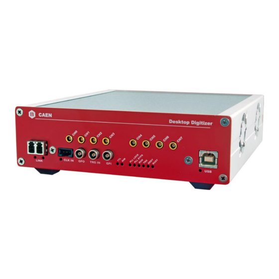
CAEN Electronic Instrumentation 4 Packaging and Compliancy DT5725 and DT5730 modules are Desktop boards housed in a 154 W x 50 H x 164 D mm³ alloy box. Fig. 4.1: Front view CAUTION: to manage the product, consult the operating instructions provided. -
Page 11: Power Requirements
Electronic Instrumentation 5 Power Requirements Both DT5725 and DT5730 modules are powered by the external AC/DC stabilized power supply provided with the digitizer and included in the delivered kit. The DT5730 typical power consumption is 2.8 A (@ +12 V). -
Page 12: Cooling Management
Bit[3] = 1 sets HIGH the fan speed. WARNING: It is recommended not to run ROC FPGA firmware revision < 4.4 on DT5730 or DT5725 with hardware revision ≥ 4 as the fans will work always at the maximum speed to prevent from hardware damages, but with a high noisiness on the other hand. -
Page 13: Temperature Protection
TEMPERATURE PROTECTION IS NOT AVAILABLE FOR DEFAULT FIRMWARE RELEASES < 4.5_0.3 (REFER TO § 13) To preserve hardware damages, DT5730 and DT5725 implement an automatic turning off of the board channels in event of internal over-temperature. Internal temperature can be monitored through register address 0x1nA8. -
Page 14: Panels Description
CAEN Electronic Instrumentation 8 Panels Description Fig. 8.1: Front panel view Fig. 8.2: Rear panel view UM3148 – DT5730/DT5725 User Manual rev. 2... -
Page 15: Front Panel
Manufacturer: AMP Inc. CML). CAEN provides single-ended to differential PINOUT A318 cable adapter (see Tab. 1.1) for CLK-IN. Coupling: AC. : 100 Ω. diff CLK IN LED (GREEN): indicates the external clock is enabled. UM3148 – DT5730/DT5725 User Manual rev. 2... - Page 16 Type: DLP 101 A 004-28. Reset) or to start/stop the acquisition. Manufacturer: FISCHER. ELECTRICAL SPECS Alternatively: Signal level: NIM or TTL. Type: EPL 00 250 NTN. Input impedance (Z ): 50 Ω. Manufacturer: LEMO. UM3148 – DT5730/DT5725 User Manual rev. 2...
- Page 17 RUN (GREEN): indicates the acquisition is running (data taking). See § Acquisition Run/Stop; TRG (GREEN): indicates the trigger is accepted. DRDY (GREEN): indicates the event/data is present in the Output Buffer. BUSY (RED): indicates all the buffers are full for at least one channel. UM3148 – DT5730/DT5725 User Manual rev. 2...
-
Page 18: Rear Panel
Manufacturer: Molveno. I → power supply ON. ELECTRICAL SPECS Not available. IDENTIFYING LABEL FUNCTION Board’s identifying label indicating: the model; the serial number (S/N); the symbol of the CE conformity marking. UM3148 – DT5730/DT5725 User Manual rev. 2... -
Page 19: Functional Description
The input bandwidth ranges from DC to 250 MHz (@3dB) for DT5730, to 125 MHz (@3dB) for DT5725, by 2 order linear phase anti-aliasing low-pass filter. -
Page 20: Clock Distribution
AD9520 configuration can be changed and stored into non-volatile memory. Changing the AD9520 configuration is primarily intended to be used for external PLL reference clock frequency change: DT5730 and DT5725 lock to an external 50 MHz clock with default AD9520 configuration (see § PLL Mode). Refer to the AD9520 datasheet for more details: http://www.analog.com/static/imported-files/data_sheets/AD9520-3.pdf... -
Page 21: Pll Mode
The Phase Detector within the AD9520 device allows to couple REF-CLK with a VCXO (500 MHz frequency) providing out the nominal ADCs frequency (500 MHz for DT5730 and 250 MHz for DT5725); for this purpose, it is necessary that REF-CLK is a submultiple of the VCXO frequency. -
Page 22: Acquisition Modes
The calibration will not need to be repeated at each run unless the operating temperature changes significantly, or clock settings are modified (e.g. switching from internal to external clock). Fig. 9.3: Typical channel before the calibration (A and B) and after the calibration (C) UM3148 – DT5730/DT5725 User Manual rev. 2... - Page 23 IMPORTANT NOTE: Starting from CAENDigitizer release 2.6.1, the Reset() function has been modified so that it no longer includes the channel calibration routine implemented in the code. This calibration must be performed on command by the dedicated Calibrate() function. Please, see the Library user manual for reference ([RD5]). UM3148 – DT5730/DT5725 User Manual rev. 2...
-
Page 24: Fig. 9.4: Automatic Calibration At Wavedump First Run
CAEN Electronic Instrumentation At software level, CAEN manages the on command channel calibration in different readout software (please, refer the relevant software User Manual for details). ➢ WaveDump 1. Lauch WaveDump. This software performs an automatic ADC calibration and displays a message when it is completed (see Fig. -
Page 25: Fig. 9.6: Channel Calibration In Dpp-Psd Control Software
3. Before to start the acquisition, monitor the channel temperatures in Tools->ADC calibration 4. Press “Calibrate” button to perform the calibration 5. Start the acquisition Fig. 9.7: Channel calibration in MC Analyzer software UM3148 – DT5730/DT5725 User Manual rev. 2... -
Page 26: Acquisition Run/Stop
(rising edge) on the TRG-IN connector. This pulse is not used as a trigger; actual triggers start from the second pulse on TRG-IN. The Stop acquisition must be SW controlled (i.e. reset of bit[2]). UM3148 – DT5730/DT5725 User Manual rev. 2... -
Page 27: Acquisition Triggering: Samples & Events
125 MHz (i.e. 8 ns or 4 ADC clock cycles in case of DT5730, while 2 ADC clock cycles in case of DT5725). Due to the way the acquired data are written into the board internal memory (i.e. in 4-sample bunches), the TTT counter is read every 2 trigger logic clock cycles, which means the trigger time stamp resolution results in 16 ns (i.e. -
Page 28: Multi-Event Memory Organization
Multi-Event Memory Organization Each channel of the DT5730/DT5725 features a SRAM memory to store the acquired events. The memory size for the event storage is 640 kS/ch or 5.12 MS/s, according to the board version (see Tab. 1.1), and it can be divided in a programmable number of buffers, N from 1 up to 1024), by register address 0x800C, as described in Tab. -
Page 29: Event Structure
(reserved otherwise), this bit is set to “1” in consequence of a hardware problem (e.g. PLL unlocking or over- temperature condition). The user can collect more information about the cause by reading at register address 0x8104 and contact CAEN Support Service if necessary (see § 14); •... -
Page 30: Event Format Example
125-MHz frequency (every 4 ADC clock cycles in case of DT5730 or 2 ADC clock cycles with DT5725). The trigger time tag value is read at half this frequency (62.5 MHz). So, the trigger time tag specifications result in 16 ns resolution and 17 s range(i.e. 8 ns*(2 -1)), which can be extended to 625 h (i.e. -
Page 31: Acquisition Synchronization
N or N-1, depending on bit[5] at register address 0x8100 as described above. It is possible to provide the BUSY signal on the digitizer front panel GPO output (bit[20], bits[19:18] and bits[17:16] at register address 0x811C are involved). UM3148 – DT5730/DT5725 User Manual rev. 2... -
Page 32: Trigger Management
A TTL or NIM external signal can be provided in the front panel TRG-IN connector (configurable at register address 0x811C). If the external trigger is not synchronized with the internal clock, a 1-clock period jitter occurs. UM3148 – DT5730/DT5725 User Manual rev. 2... -
Page 33: Self-Trigger
(depending on the trigger polarity bit at register address 0x8000). THRESHOLD CH0 IN over-threshold signal [0] under-threshold signal [0] Fig. 9.11: Channel over/under threshold signal UM3148 – DT5730/DT5725 User Manual rev. 2... -
Page 34: Fig. 9.12: Channel Pulse Signal
Previous firmware don’t implement the register address 0x1n84 as well as the 0x1n70, the self-trigger is intended only as the over/under threshold signal and a trigger request is intended only as the OR of the self-triggers couple. UM3148 – DT5730/DT5725 User Manual rev. 2... -
Page 35: Trigger Coincidence Level
= 00 (i.e. Majority level = 0), which means the coincidence acquisition mode is disabled and the T TVAW meaningless. In this case, the board common trigger is simple OR of the signals from the enabled channels pairs. UM3148 – DT5730/DT5725 User Manual rev. 2... -
Page 36: Fig. 9.13: Trigger Request Management At Mezzanine Level With Majority Level = 0
Fig. 9.13: Trigger request management at mezzanine level with Majority level = 0 TRG_REQ [0] TRG_REQ [1] ORed signal COMMON TRIGGER (Maj. Lev. = 0) Fig. 9.14: Trigger request management at motherboard level with Majority level = 0 UM3148 – DT5730/DT5725 User Manual rev. 2... -
Page 37: Fig. 9.15: Trigger Request Relationship With Majority Level = 1 And T
Note: with respect to the position where the common trigger is generated, the portion of input signal stored depends on the programmed length of the acquisition window and on the post trigger setting. UM3148 – DT5730/DT5725 User Manual rev. 2... - Page 38 In this case, the common trigger is issued if at least two of the enabled trigger requests are instantaneously in coincidence (no TTVAW is waited). Note: a practical example of making coincidences with the digitizer in the standard operating is detailed in [RD11]. UM3148 – DT5730/DT5725 User Manual rev. 2...
-
Page 39: Trigger Distribution
Fig. 9.17: Trigger configuration on GPO front panel output connector The registers involved in the GPO programming are: Register address 0x8110; Register address 0x811C. Note: Refer to [RD2] for registers complete description. UM3148 – DT5730/DT5725 User Manual rev. 2... -
Page 40: Example
Register 0x810C on all the boards in the system (including board “n”): Enable External Trigger to participate in the board’s common acquisition trigger, disable Software Trigger and the Trigger Requests from the channels (bits[31:30] = 01; bits[3:0] = 0000). UM3148 – DT5730/DT5725 User Manual rev. 2... -
Page 41: Reset, Clear And Default Configuration
The Timer Reset allows to initialize the timer which allows to tag an event. The Timer Reset can be forwarded with a pulse sent to the front panel GPI input (leading edge sensitive). UM3148 – DT5730/DT5725 User Manual rev. 2... -
Page 42: Data Transfer Capabilities
Data Transfer Capabilities DT5730 and DT5725 feature a Multi-Event digital memory per channel, configurable by the user to be divided into 1 up to 1024 buffers, as detailed in § Multi-Event Memory Organization. Once they are written in the memory, the events become available for readout via USB or Optical Link. -
Page 43: Optical Link And Usb Access
(communication path which uses optical fiber cables as physical transmission line) providing transfer rate up to 80 MB/s. The latter allows to connect up to 8 DT5730/DT5725 boards to a single A2818 PCI Optical Link Controller or up to 32 boards to a single A3818 PCIe Optical Link Controller. Detailed information on CAEN PCI/PCIe Controllers can be find at www.caen.it:... -
Page 44: Drivers & Libraries
(communication, configuration, readout, etc.): • CAENVMELib is a set of ANSI C functions which permit a user program to use and configure the CAEN Bridges and Controllers V1718/VX1718 (VME-USB2.0 Bridge), V2718/VX2718 (VME-PCI/PCIe Optical Link Bridge), A2818/A3818 (PCI/PCIe-CONET Controller). -
Page 45: Fig. 10.1: Required Libraries And Drivers
DT5730/DT5725 Fig. 10.1: Required libraries and drivers If required to be installed apart by the user (see § 11), CAEN Libraries are available for download on CAEN web site (www.caen.it) in the “Download” tab at the library web page: Home / Products / Firmware/Software / Digitizer Software / Software Libraries / <CAEN Library>... -
Page 46: Software Tools
CAEN Electronic Instrumentation 11 Software Tools CAEN provides software tools to interface the DT5730/DT5725, which are available for free download on www.caen.it Home / Products / Firmware/Software / Digitizer Software CAENUpgrader CAENUpgrader is a free software composed of command line tools together with a Java Graphical User Interface. -
Page 47: Caencomm Demo
CAENComm Demo can operate with Windows OSs, 32 and 64-bit. It requires CAENComm and CAEVMElib libraries as additional software to be installed (see § 10). The Demo is included in the CAENComm library installation Windows package, which can be downloaded on CAEN web site (login required) at: Home / Products / Firmware/Software / Digitizer Software / Software Libraries / CAENComm Library UM3148 –... -
Page 48: Caen Wavedump
Electronic Instrumentation CAEN WAVEDump WaveDump is a basic console application, with no graphics, supporting only CAEN digitizers running the default firmware. It allows the user to program a single board (according to a text configuration file containing a list of parameters and instructions), to start/stop the acquisition, read the data, display the readout and trigger rate, apply some post-processing (e.g. -
Page 49: Fig. 11.4: Caenscope Main Frame
Linux needs the required libraries to be previously installed by the user. The installation packages can be downloaded on CAEN web site (login required) at: Home / Products / Firmware/Software / Digitizer Software / Readout Software / CAENSCOPE The reference document for installation instructions and program detailed description is [RD8], downloadable at the same page above, in the Documentation tab. -
Page 50: Dpp-Psd Control Software
Electronic Instrumentation DPP-PSD Control Software The DT730 and DT5725 can be equipped (on payment) with a special DPP-PSD firmware. DPP-PSD Control Software is a software interface for configuration, acquisition, data plotting to be used with the digitizers who can run the DPP-PSD special firmware. It allows the user to set the parameters for the acquisition, to configure the DPP, to perform the data readout, the histogram collection and the spectrum or waveform plotting and saving. -
Page 51: Fig. 11.6: Mc²Analyzer (Mc²A) Software Tool
Fig. 11.6: MC²Analyzer (MC²A) software tool MC²Analyzer is currently available only for Windows platforms. The installation package can be downloaded on CAEN web site (www.caen.it) at: Home / Products / Firmware/Software / Digitizer Software / Readout Software The reference document for installation instructions and program detailed description is [RD10]. -
Page 52: Hw Installation
Power-on Sequence To power on the board, follow the procedure below: 1. connect the 12V DC power supply to the DT5730/DT5725 through the DC input rear connector; 2. power up the DT5730/DT5725 through the ON/OFF rear switch. See § Rear Panel to identify the relevant components... -
Page 53: Firmware And Upgrades
The user can so perform a further upgrade attempt on the STD page to restore the firmware copy. At power-on, if the user cannot communicate with the board, it needs to be sent back to CAEN in repair (see § 14). -
Page 54: Default Firmware Upgrade
(30 minutes). Details on the license ordering procedure can be found in [RD1]. Note: if the DPP firmware license is included in the same order of a DT5730 (DT5725), the customer will be delivered ... -
Page 55: Technical Support
CAEN Electronic Instrumentation 14 Technical Support CAEN support services are available for the user by accessing the Support & Services area on CAEN website at www.caen.it. Returns and Repairs Users who need for product(s) return and repair have to fill and send the Product Return Form (PRF) in the Returns and Repairs area at Home / Support &... - Page 56 UM3148 - DT5730/DT5725 - User Manual rev. 2 - 10 June 2016 00108-12-DT5730-MUTX Copyright © CAEN SpA. All rights reserved. Information in this publication supersedes all earlier versions. Specifications subject to change without notice. UM3148 – DT5730/DT5725 User Manual rev. 2...
Need help?
Do you have a question about the DT5725 and is the answer not in the manual?
Questions and answers