
Related Manuals for Caen N6724


Summary of Contents for Caen N6724
- Page 1 User Manual UM3247 N6724 2/4 Channel 14bit 100 MS/s Waveform Digitizer Rev. 10 - January 27 , 2017...
-
Page 2: Purpose Of This Manual
Purpose of this Manual This document contains the full hardware descrip on of the N6724 CAEN digi zer and their principle of opera ng as Waveform Recording Digi zer (basing on the herea er called ”waveform recording firmware”). The reference firmware revision is: 4.12_0.14. - Page 3 The informa on contained herein has been carefully checked and is believed to be accurate; however, no responsi- bility is assumed for inaccuracies. CAEN SpA reserves the right to modify its products specifica ons without giving any no ce; for up to date informa on please visit www.caen.it.
-
Page 4: Table Of Contents
Example ..........UM3247 - N6724 User Manual rev. 10... - Page 5 CAEN WaveDump ........
- Page 6 Fig. 9.3 CAEN WaveDump ........
-
Page 7: Safety No Ces
USE ONLY CRATES WITH FORCED COOLING AIR FLOW SINCE OVERHEATING THE BOARD MAY DEGRADE ITS PERFORMANCES! CAUTION: this product needs proper handling. N6724 DOES NOT SUPPORT LIVE INSERTION (HOT SWAP)! REMOVE OR INSERT THE BOARD WHEN THE NIM CRATE IS POWERED OFF! -
Page 8: Introduc On
1 Introduc on The Mod. N6724 is a 1-unit wide NIM module housing a 2/4 Channel 14 bit 100 MS/s Desktop Waveform Digi zer with 2.25 V input dynamic range on single ended MCX coaxial connectors. Customized versions of 10 V and 500 mV input range are available (see Tab. -
Page 9: Tab. 1.1 Table Of Models And Related Items
Op cal Fibre 30 cm simplex AY2730 Op cal Fibre 30 m duplex AY2720 Op cal Fibre 20 m duplex AY2705 Op cal Fibre 5 m duplex Tab. 1.1: Table of models and related items UM3247 - N6724 User Manual rev. 10... -
Page 10: Block Diagram
CLOCK CLK IN MANAGER (AD9520) TRG IN ROC [FPGA] - Readout control - Optical link control - USB interface control - Trigger control OPTICAL LINK - External interface control Fig. 2.1: Block Diagram UM3247 - N6724 User Manual rev. 10... -
Page 11: Technical Specifica Ons
- 10 s range; 64 bit sw - So ware-trigger: common trigger by extension so ware command DPP-DAW: 31-bit counter – 10 ns resolu on - 21 s range; 64 bit sw extension UM3247 - N6724 User Manual rev. 10... -
Page 12: Tab. 3.1 Specifica On Table
General purpose C libraries, configura on tools, readout so ware (Windows® and SOFTWARE Linux® support). LabVIEW™ VIs and demos for Windows® only POWER 3.9A @ +6V, 90mA @ -6V CONSUMPTIONS Tab. 3.1: Specifica on table UM3247 - N6724 User Manual rev. 10... -
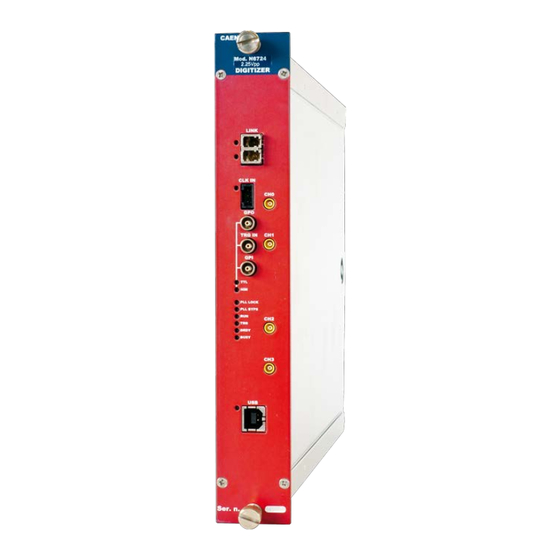
Page 13: Packaging And Compliancy
4 Packaging and Compliancy The module is housed in a single-width NIM unit. Fig. 4.1: Front view Fig. 4.2: Side view UM3247 - N6724 User Manual rev. 10... - Page 14 ALL CABLES MUST BE REMOVED FROM THE FRONT PANEL BEFORE EXTRACTING THE BOARD FROM THE CRATE! CAEN provides the specific document “Precau ons for Handling, Storage and Installa- on”, available in the documenta on tab of the product’s web page, that it is manda- tory to read before operating with CAEN equipment.
-
Page 15: Power Requirements
5 Power Requirements The table below resumes the N6724 power consump ons per relevant power supply rail. MODULE SUPPLY VOLTAGE +6 V -6 V N6724 3.9 A 90 mA Tab. 5.1: Power requirements table UM3247 - N6724 User Manual rev. 10... -
Page 16: Panels Descrip On
6 Panels Descrip on Fig. 6.1: Front panel view UM3247 - N6724 User Manual rev. 10... -
Page 17: Front Panel
Run signal, ClkOut signal, ClockPhase signal, PLL_Unlock signal or Busy signal according to register address 0x811C. ELECTRICAL SPECS Signal level: NIM or TTL. Requires 50 Ω termina on. UM3247 - N6724 User Manual rev. 10... - Page 18 Type: 787780-2 (B-Type). Manufacturer: AMP Inc. ELECTRICAL SPECS Standard: compliant with USB 2.0 and USB 1.0. Transfer rate: up to 30 MB/s. USB LINK LED (GREEN): indicates the USB communica on is ac ve. UM3247 - N6724 User Manual rev. 10...
- Page 19 - Manufacturer name and func onal name - Module name and the input range informa on A li le silver label on the bo om of the NIM front panel reports: - Serial Number (S/N) UM3247 - N6724 User Manual rev. 10...
-
Page 20: Func Onal Descrip On
DC Offset Individual Setting Se ng the DC offset for channel n requires a write access at register addresses 0x1n98 [RD1]. Wri ng at 0x8098, the DC offset will apply to all channels at once. UM3247 - N6724 User Manual rev. 10... -
Page 21: Clock Distribu On
The external clock signal must be differen al (LVDS, ECL, PECL, LVPECL, CML) with a ji er lower than 100 ppm (see Chap. Technical Specifica ons). CAEN provides the A318 cable to adapt single ended signals coming from an external clock unit into the differen al CLK-IN connector (see Tab. 1.1). -
Page 22: Pll Mode
If the digi zer is locked, the PLL-LOCK front panel LED must be on. Note: the user who wants to work as in point 3, please contact CAEN (see Chap. Technical Support) indicat- ing the required reference clock frequency, to check its feasibility and then receive the PLL programming file. -
Page 23: Decima On
= [0, 1, , 7]. The n parameter is set through the register address 0x8044 [RD1]. Trigger Clock The TRG-CLK logic works at 100 MHz, equal to the sampling frequency: TRG-CLK = SAMPL-CLK. UM3247 - N6724 User Manual rev. 10... -
Page 24: Acquisi On Modes
Sec. Acquisi on Run/Stop) or with respect to a buffer emptying a er a Memory FULL status (see Sec. Acquisi on Synchroniza on). - The trigger overlaps the previous one and the board is not enabled for accep ng overlapped triggers. UM3247 - N6724 User Manual rev. 10... -
Page 25: Fig. 7.3 Trigger Overlap
EVENT COUNTER value iden fies the trigger number sent (but the event number sequence is lost); if the func on is not enabled, the EVENT COUNTER value coincides with the sequence of buffers saved and readout. UM3247 - N6724 User Manual rev. 10... -
Page 26: Mul -Event Memory Organiza On
Multi-Event Memory Organization Each channel of the N6724 features a SRAM memory to store the acquired events. The memory size for the event storage is 512 kS/ch or 4 MS/ch, according to the board version (see Tab . 1.1), and it can be divided in a programmable number of buffers, N... -
Page 27: Event Structure
(reserved otherwise), it is set to “1” in consequence of a hardware problem (e.g. PLL unlocking). The user can collect more informa on about the cause by reading at register address 0x8104 and contact CAEN Support Service if necessary (see Chap. Technical Support). • ZLE FLAG (bit[24] of 2 header word) indicates whether the ZLE suppression mode is enabled (1) or not (0) (see Sec. -
Page 28: Data
Data are the stored samples. Data from masked channels are not read. Event Format Examples Figure 7.4 shows the data format in case all the 4 channels are enabled, with Zero Length Encoding disabled and enabled respec vely. UM3247 - N6724 User Manual rev. 10... -
Page 29: Fig. 7.4 Event Format
SAMPLE [N-2 ] – CH [1] SIZE CONTROL WORD SAMPLE [1] – CH[3] SAMPLE [0] – CH[3] CONTROL WORD SAMPLE [N-1] – CH[3] SAMPLE [N-2 ] – CH [3] Fig. 7.4: Event Format UM3247 - N6724 User Manual rev. 10... -
Page 30: Acquisi On Synchroniza On
0x8100 as above described. It is possible to provide the BUSY signal on the digi zer front panel GPO output (bit[20], bits[19:18] and bits[17:16] at register address 0x811C are involved [RD1]). UM3247 - N6724 User Manual rev. 10... -
Page 31: Zero Suppression
• Full Suppression based on the integral of the signal (ZS_INT). • Full Suppression based on the signal amplitude (ZS_AMP). • Zero Length Encoding (ZLE). The user can select the zero suppression algorithm by se ng bits[19:16] of register 0x8000 [RD1]. UM3247 - N6724 User Manual rev. 10... -
Page 32: Full Suppression Based On The Integral Of The Signal
31 30 29 28 27 26 25 24 23 22 21 20 19 18 17 16 15 14 13 12 11 10 9 8 7 6 5 4 3 2 1 0 . . . Channel Mask = 0x5 ..Fig. 7.5: Zero Suppression based on the integral. UM3247 - N6724 User Manual rev. 10... -
Page 33: Full Suppression Based On The Amplitude Of The Signal
31 30 29 28 27 26 25 24 23 22 21 20 19 18 17 16 15 14 13 12 11 10 9 8 7 6 5 4 3 2 1 0 . . . Channel Mask = 0x5 ..Fig. 7.6: Zero Suppression based on the amplitude. UM3247 - N6724 User Manual rev. 10... -
Page 34: Zero Length Encoding Zle
). Within the good area there are the samples back, the over-threshold SKIP GOOD and the samples forward (N , and N respec vely). The bo om figure shows the corresponding LFWD event structure. UM3247 - N6724 User Manual rev. 10... -
Page 35: Fig. 7.8 Zero Suppression Based On The Zero Length Encoding
. . . Channel Mask = 0x1 SIZE CH0 RESERVED SKIP1 RESERVED GOOD1 SAMPLES GOOD1 RESERVED SKIP2 RESERVED GOOD2 SAMPLES GOOD2 RESERVED SKIP3 Fig. 7.8: Zero Suppression based on the Zero Length Encoding. UM3247 - N6724 User Manual rev. 10... -
Page 36: Zle Examples
, and N = 0. LFWD ≤ N Analogously, in case N = 0 and N overlaps with N < N ), all samples of N LFWD LFWD tagged as good and acquired (N GOOD2 UM3247 - N6724 User Manual rev. 10... -
Page 37: Lbk Lfwd
31 30 29 28 27 26 25 24 23 22 21 20 19 18 17 16 15 14 13 12 11 10 9 8 7 6 5 4 3 2 1 0 . . . SIZE CHx RESERVED RESERVED GOOD1 SAMPLES GOOD1 RESERVED GOOD2 SAMPLES GOOD2 RESERVED Fig. 7.12: Example with posi ve logic and N overlapping with N UM3247 - N6724 User Manual rev. 10... -
Page 38: Trigger Management
A TTL or NIM external signal can be provided to the front panel TRG-IN connector (configurable at register address 0x811C). If the external trigger is not synchronized with the internal clock, a 1-clock period ji er occurs. UM3247 - N6724 User Manual rev. 10... -
Page 39: Self-Trigger
Over-threshold signal from CHn SELF_TRG Under-threshold signal from CHn Fig. 7.14: Self-trigger genera on. Bits[3:0] of register 0x810C allows the user to program which channel par cipates to the global trigger genera on. UM3247 - N6724 User Manual rev. 10... -
Page 40: Trigger Coincidence Level
Note: with respect to the posi on where the common trigger is generated, the por on of input signal stored depends on the programmed length of the acquisi on window and on the post trigger se ng. UM3247 - N6724 User Manual rev. 10... -
Page 41: Fig. 7.16 Self-Trigger Rela Onship With Majority Level = 1 And T
Fig. 7.17 shows the trigger management in case the coincidences are enabled with Majority level = 1 and = 0 (i.e. 1 clock cycle). TVAW Note: CAEN provides a guide to coincidences including a prac cal example of making coincidences with the waveform recording firmware [RD5]. UM3247 - N6724 User Manual rev. 10... -
Page 42: Fig. 7.17 Self-Trigger Rela Onship With Majority Level = 1 And Ttvaw = 0
CH0 THRESHOLD CH0(enabled) IN SELF-TRG[CH0] CH1 THRESHOLD CH1(enabled) IN SELF-TRG[CH1] OR signal TVAW TRIGGER (Maj.lev = 1) Fig. 7.17: Self-trigger rela onship with Majority level = 1 and T = 0. TVAW UM3247 - N6724 User Manual rev. 10... -
Page 43: Trg-In As Gate
- the OR of all the enabled trigger sources (only the So ware Trigger is provided by default, as in the red path of Fig. 7.18); - the OR, AND or MAJORITY exclusively of the channel self-triggers. The registers involved in the GPO programming are: - Register address 0x8110; - Register address 0x811C. UM3247 - N6724 User Manual rev. 10... -
Page 44: Example
(board “n”) crosses its threshold. Trigger Out signal is then fed to an external Fan Out logic unit (e.g. CAEN V2495 board); the obtained signal has then to be provided to the external trigger input TRG-IN of all the boards in the system (including the board which generated the Trigger Out signal). -
Page 45: Global Reset
Timer Reset The Timer Reset allows to ini alize the mer which tags an event. The Timer Reset can be forwarded with a pulse sent either to the GPI input (leading edge sensi ve). UM3247 - N6724 User Manual rev. 10... -
Page 46: Block Transfer
It is suggested, a er the 1st word is transferred, to check the EVENT SIZE informa on and then do as many cycles as necessary (actually EVENT SIZE -1) in order to read completely the event. UM3247 - N6724 User Manual rev. 10... - Page 47 Op cal Link (communica on path which uses op cal fiber cables as physical transmission line) able to transfer data at 80 MB/s, therefore it is possible to connect up to eight N6724 to a single Op cal Link Controller by using the A2818 PCI card or up to thirty-two N6724 with the A3818 PCIe card.
-
Page 48: Drivers & Libraries
[RD8]. Libraries CAEN libraries are a set of middleware so ware required by CAEN so ware tools for a correct func oning. These libraries, including also demo and example programs, represent a powerful base for users who want to develop customized applica ons for the digi zer control (communica on, configura on, readout, etc.): •... -
Page 49: Fig. 8.1 Drivers And So Ware Layers
DLL files of the required libraries. LINUX® compliant CAEN so ware = YES. CAEN so ware for Linux® OS is not stand-alone. The user must install the required libraries apart to run the so ware. The only no ceable excep on is the CAENDPPLib library which is stand-alone also for LINUX®. -
Page 50: So Ware Tools
9 So ware Tools CAEN provides so ware tools to interface the 724 digi zer family, which are available for free download at www.caen.it following the path: Home / Products / Firmware/So ware / Digi zer So ware CAENUpgrader CAENUpgrader is free so ware composed of command line tools together with a Java Graphical User In- terface. -
Page 51: Caencomm Demo
CAEN web site (login required) at: Home / Products / Firmware/So ware / Digi zer So ware / So ware Libraries / CAENComm Library CAEN provides the Demo descrip on in the CAENComm library User Manual, free downloadable at the web page above. -
Page 52: Caen Wavedump
Home / Products / Firmware/So ware / Digi zer So ware / Readout So ware / CAEN WaveDump CAEN provides the so ware User Manual [RD9] and a guide for ge ng started with it, free downloadable at the web page above. -
Page 53: Caen Scope
CAEN Scope In a brand new framework, CAENScope so ware allows to manage the CAEN digi zers running the wave- form recording firmware. CAENScope user friendly interface presents different sec ons to easily manage the digi zer configura on and plot the waveforms. Once connected, the program retrieves the digi zer informa on. Different pa- rameters can be set for the channels, trigger and trace visualiza on (up to 12 traces) can be simultaneously plo ed. -
Page 54: Caen Mc
Home / Products / Firmware/So ware / Digi zer So ware / Readout So ware / MC Analyzer CAEN provides the so ware User Manual [RD3], free downloadable at the web page above. Note: MC Analyzer is currently available only for Windows® OS, all required libraries are installed locally with the program;... -
Page 55: Fig. 9.6 Compass So Ware Tool
CoMPASS CoMPASS (CAEN Mul -PArameter Spectroscopy So ware) is the new so ware from CAEN able to imple- ment a Mul -parametric DAQ for Physics Applica ons, where the detectors can be connected directly to the digi zers inputs and the so ware acquires energy, ming, and PSD spectra. -
Page 56: Hw Installa On
USE ONLY CRATES WITH FORCED COOLING AIR FLOW SINCE OVERHEATING THE BOARD MAY DEGRADE ITS PERFORMANCES! CAUTION: this product needs proper handling. N6724 DOES NOT SUPPORT LIVE INSERTION (HOT SWAP)! REMOVE OR INSERT THE BOARD WHEN THE NIM CRATE IS POWERED OFF! -
Page 57: Power-On Sequence
Power-on Sequence To power on the board, perform the following steps: 1. Insert the N6724 into the crate; 2. power up the crate. Power-on Status At power-on, the module is in the following status: • the Output Buffer is cleared;... -
Page 58: Firmware And Upgrades
All firmware updates are available for download on CAEN website www.caen.it (login required) at the following path: Home / Products / Modular Pulse Processing Electronics / NIM / Digi zers / N6724 Different firmware are available for the 724 family: •... -
Page 59: Troubleshooting
When a failure occurs during the upgrade of the STD page of the FLASH, which compromises the commu- nica on with the N6724 , the user can perform the following recovering procedure as first a empt: - force the board to reboot loading the copy of the firmware stored on the BKP page of the FLASH. -
Page 60: Technical Support
12 Technical Support CAEN support services are available for the user by accessing the Support & Services area on CAEN website at h p://www.caen.it. Returns and Repairs Users who need for product(s) return and repair have to fill and send the Product Return Form (PRF) in the Returns and Repairs area at Home / Support &... - Page 61 UM3247 - N6724 User Manual rev. 10- January 27 th , 2017 00000-00-02827-GXXX Copyright ©CAEN SpA. All rights reserved. Informa on in this publica on supersedes all earlier versions. Specifica ons subject to change without no ce.
Need help?
Do you have a question about the N6724 and is the answer not in the manual?
Questions and answers