Table of Contents
Advertisement
Quick Links
CAUTION:
Before servicing this chassis, it is important that the service technician read the "Safety
Precautions" and "Product Safety Notices" in this service manual.
ATTENTION:
Avant d'effectuer l'entretien du châassis, le technicien doit lire les «Précautions de sécurité»
et les «Notices de sécurité du produit» présentés dans le présent manuel.
VORSICHT:
Vor Öffnen des Gehäuses hat der Service-Ingenieur die „Sicherheitshinweise" und „Hinweise
zur Produktsicherheit" in diesem Wartungshandbuch zu lesen.
SPECIFICATIONS AND PARTS ARE SUBJECT TO CHANGE FOR IMPROVEMENT
SERVICE MANUAL
MANUEL D'ENTRETIEN
WARTUNGSHANDBUCH
Digital Versatile Disk
August 2004
Downloaded Free from http://www.free-service-manuals.com
No. 9403
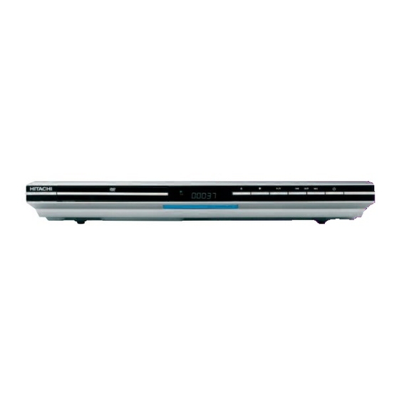
DV-P345UK
DV-P345E
Data contained within this Service
manual is subject to alteration for
improvement.
Les données fournies dans le présent
manuel d'entretien peuvent faire l'objet
de modifications en vue de perfectionner
le produit.
Die in diesem Wartungshandbuch
enthaltenen Spezifikationen können sich
zwecks Verbesserungen ändern.
Advertisement
Table of Contents

Related Manuals for Hitachi DV-P345E


Summary of Contents for Hitachi DV-P345E
- Page 1 No. 9403 DV-P345UK DV-P345E SERVICE MANUAL MANUEL D'ENTRETIEN WARTUNGSHANDBUCH CAUTION: Before servicing this chassis, it is important that the service technician read the “Safety Precautions” and “Product Safety Notices” in this service manual. Data contained within this Service manual is subject to alteration for improvement.
-
Page 2: General Description
1. G ENERAL ESCRIPTION 1.1 ZR36768 The ZR36768 Disc Loader Controller and Decoder Device can control disc loaders and read bitstreams using the following media: DVD-ROM, DVDRW, CD-DA, CD-ROM, CD-R and CD-R/W discs. The device can decode bitstreams and process navigation data of the following formats: DVD-Video, DVD-Audio, CD-DA, VCD (Video-CD), SVCD (Super Video-CD) and MP3. -
Page 3: Drive Interfaces
• Letterbox and Pan-scan display aspect ratio conversion (16:9 to 4:3) • Automatic frame rate conversion (e.g., 3/2 pull down) and format conversion (16:9, 4:3, 1:1). • EIA-608 compatible modulation of line 21 (NTSC) or line 22 (PAL) closed captions data over the video output. - Page 4 1.5 R ANEL A typical rear panel supports: - Six channel or two channel audio outputs - Optical and coax S/PDIF outputs. - Composite, S-Video, and SCART outputs Outputs provided by ZR36768 are Composite, Y/C, YUV or RGB interlaced analog video output or component progressive analog video output (using 10 bits on-chip DACs).
- Page 5 SDATA[2] // I // SERVO channel sample data input for AFE by-pass // PM[2] Probe mux data output 149,147 GPCI/O[34-31] I/O General purpose input/output pins, monitored/controlled by the CPU or DSP 145,136 ICGPCI/O[5,4] I/O General purpose input/output pins monitored/controlled by the CPU or DSP 148,146 SW.
- Page 6 DACTEST[6] DACs test input VID[5] // O // Digital video luma/chroma output, multiplexed in time according to the CCIR656 standard (for interlaced video) or luma (for progressive) // ICETDO // O // ADP debug interface // DJTDO // O // DSP debug interface // IDGPCI/O[1]// I/O //...
- Page 7 SW. When input, the pin can be used as general purpose external interrupt to the CPU // CJTMS // I // CPU debug interface // DACTEST[10] // I // DACs test input // PM[11] Probe mux data output HSYNC# // O // Digital video horizontal sync signal// GPCI/O[25]//...
- Page 8 PWMACT[0] O // PWM0 output signal // GPCI/O[39] I/O // General purpose input/output pin, monitored/controlled by the CPU or DSP SW // DVDDAT[0] I // DVD-DSP data input for FE by-pass // NRZDATA NRZ data input for AFE and DRC by-pass PWMACT[1] O // PWM1 output signal //...
- Page 9 RFDAT[4] RF channel sample data inputs for AFE by-pass ICGPCI/O[7] // I/O // General purpose input/output pin, monitored/controlled by the CPU or DSP SW. When input, the pin can be used as general purpose external interrupt to the CPU // DVDERR // I // DVD-DSP error input for FE by-pass.
- Page 10 SW // PM[15] Probe mux data output SSCCLK // I/O // SSC clock input signal or output // GPCI/O[47] // I/O // General purpose input/output pin, monitored/controlled by the CPU or DSP SW // PM[13] Probe mux data output PNVM/SRAM Interface (41 pins) 9,14,18, MEMDA[15-0] PNVM/SRAM bidirectional data bus...
- Page 11 MEMCS[0]# PNVM/SRAM chip select (active low) output MEMCS[1]# // O // PNVM/SRAM chip select (active low) output// GPCI/O[18] General purpose input/output pin, monitored/controlled by the CPU or DSP Power Signals (56 pins) 12,32,50 GNDP Digital periphery ground of 3.3 V supply (12 pins) ,62,72,8 3,91,101 ,107,125...
-
Page 12: System Block Diagram
2.1 SYSTEM BLOCK DIAGRAM A sample system block diagram for the MT1379 DVD player board design is shown in the following figure: 3. A UDIO UTPUT The ZR36768 supports two-channel to eight-channel analog audio output. This version has two- channel output. The ZR36768 also provides digital output in S/PDIF format. -
Page 13: Flash Memory
The image post-processing unit can scale the stored image (horizontally and vertically with scale ratios of 1/2 to 2) and shift it with 1/4 pixel resolution. Then, it can enhance the image and pad it with background colour. In addition, the VPU has a DVD sub-picture decoding unit. The sub-picture is blended with the enhanced image. -
Page 14: Vfd Controller
9. PLL - P ROCESSING LOCK ENERATION The PLL unit consists of three sub-units: The PLLa unit generates (under ADP control) the audio interface master clock (AMCLK). It has 13 bits of frequency multiply and divide factors. Its input can be a separate clock generator or be (externally) tied to the clock generator or crystal input to the processing clock PLL (see below). - Page 15 16 à Fast Blanking 17 à Video Gnd 18 à Fast Blanking Gnd 19 à Composite Video In 20 à Composite Video Out 21 à Shield Some cheaper SCART cables use unshielded wires, which is just about acceptable for short cable lengths. For longer lengths, shielded co-ax cable become essential. Scart Signals: Audio signals 0.5V RMS, <1K output impedance, >10K input impedance.
-
Page 16: Circuit Description
CIRCUIT DESCRIPTION 12.1 POWER SUPPLY: • Socket PL2 is the 220VAC input. • 2.5A fuse F1 is used to protect the device against short circuit. • Line filters and capacitors L1, C1, L5 and L6 are used to block the parasitic coming from the mains. - Page 17 • TOTX176 is used for laser output. • For coaxial audio output SPDIF is used. • Q4, Q5, Q6, Q7, Q8 and Q9 transistors are to mute the audio outputs while switching the state of the unit(power on/off) • There are two op-amps in U9, U12 and U14. They are used for left,right,rear left and right, subwoofer center audio channels.
- Page 18 VFD Type: O = Old VFD / N = New small VFD / T = TV DVD/7 NoVFD OPU Type: A = ASA SANYO HD60 / F = FUSS HITACHI HOP 1200 DAC Type: A6 = AK4356 / A2 = AK4382 / P6 = PCM1606 / C2 = CS4392 Example: A6AO1.bin = AK4356, ASA, OLD VFD,Language Group 1...
- Page 19 11) When CD update is finished tray is closed, screen is refreshed, update is finished. 12) To see Version Page; - Press DISPLAY button from remote - Press “1”-“3”-“5”-“7” at Setup Menu Setup Menu screen refresh and “Version” selection can be seen under “Preferences Setup” - Select “Version”or version Page 1st line contains release number like EFXX line contains hardware options and build number...
- Page 20 THE UPDATED PARTS LIST FOR THIS MODEL IS AVAILABLE ON ESTA Downloaded Free from http://www.free-service-manuals.com...
- Page 21 14.CIRCUIT SCHEMATICS: No. 9403 MAIN BOARD SHEET 1 Downloaded Free from http://www.free-service-manuals.com...
- Page 22 No. 9403 MAIN BOARD SHEET 2 Downloaded Free from http://www.free-service-manuals.com...
- Page 23 No. 9403 MAIN BOARD SHEET 3 Downloaded Free from http://www.free-service-manuals.com...
- Page 24 No. 9403 MAIN BOARD SHEET 4 Downloaded Free from http://www.free-service-manuals.com...
- Page 25 No. 9403 MAIN BOARD SHEET 5 Downloaded Free from http://www.free-service-manuals.com...
- Page 26 No. 9403 MAIN BOARD SHEET 6 Downloaded Free from http://www.free-service-manuals.com...
- Page 27 No. 9403 MAIN BOARD SHEET 7 Downloaded Free from http://www.free-service-manuals.com...
-
Page 28: Power Supply Board
No. 9403 POWER SUPPLY BOARD Downloaded Free from http://www.free-service-manuals.com... - Page 29 No. 9403 FP BOARD Downloaded Free from http://www.free-service-manuals.com...
-
Page 30: Main Board
15.CIRCUIT BOARDS: COMPONENT (TOP) SIDE SOLDER (BOTTOM) SIDE No. 9403 MAIN BOARD Downloaded Free from http://www.free-service-manuals.com... -
Page 31: Power Board
SOLDER (BOTTOM) SIDE COMPONENT (TOP) SIDE COMPONENT SOLDER (TOP) SIDE (BOTTOM) SIDE SCART BOARD FRONT PANEL BOARD COMPONENT (TOP) SIDE POWER BOARD No. 9403 POWER, FP & SC BOARDS Downloaded Free from http://www.free-service-manuals.com... - Page 32 Fax: +46 (0) 8 562 711 13 Tel: +39 02 38073415 Servizio Clienti Email: csgswe@hitachi-eu.com Fax: +39 02 48786381/2 Email: customerservice.italy@hitachi-eu.com HITACHI EUROPE S.A.S HITACHI EUROPE LTD (Norway) AB Lyon Office STRANDVEIEN 18 B.P. 45, 69671 BRON CEDEX 1366 Lysaker FRANCE...
Need help?
Do you have a question about the DV-P345E and is the answer not in the manual?
Questions and answers