Table of Contents
Advertisement
このサービスマニュアルはエコパルプ
(ECF:無塩素系漂白パルプ)を使用しています。
011652
PA
PC9500N: 20020925-400000
PC4800N: 20020925-330000
POWER AMPLIFIERS
SERVICE MANUAL
CONTENTS
(目次)
(総合仕様)
(パネルレイアウト)
(ブロックダイアグラム)
(結線図)
..................................................................... 8
(寸法図)
DIMENSIONS
(LSI端子機能表)
(ICブロック図)
(シート基板図)
(検査)
................................................ 3/4
.................................... 5
.............................. 6
.......................................................... 10
(分解手順)
............................ 11
.............................. 16
................................. 17
....................................... 19
...................................................... 30/37
(総回路図)
HAMAMATSU, JAPAN
1.361K-3611
PC9500N/PC4800N
PC9500N
1
Printed in Japan 2002.9
Advertisement
Table of Contents

Related Manuals for Yamaha PC4800N


Summary of Contents for Yamaha PC4800N
- Page 1 LSI PIN DESCRIPTION (LSI端子機能表) ......16 (ICブロック図) IC BLOCK DIAGRAM ......... 17 (シート基板図) CIRCUIT BOARDS ........19 INSPECTIONS (検査) ............30/37 PARTS LIST このサービスマニュアルはエコパルプ (総回路図) OVERALL CIRCUIT DIAGRAMS (ECF:無塩素系漂白パルプ)を使用しています。 011652 HAMAMATSU, JAPAN PC9500N: 20020925-400000 1.361K-3611 Printed in Japan 2002.9 PC4800N: 20020925-330000...
- Page 2 IMPOR TANT NOTICE This manual has been provided for the use of authorized Yamaha Retailers and their service personnel. It has been assumed that basic service procedures inherent to the industry, and more specifically Yamaha Products, are already known and under- stood by the users, and have therefore not been restated.
- Page 3 Power cord, Security cover, Owner’s Manual, Euroblock connector (2) 0 dB=0.775 Vrms, Half Power=1/2 Power Output Level (Rated Power) For European Model Purchaser/User information specified in EN55103-1 and EN55103-2. Inrush Current: 20A (PC9500N) / 25A (PC4800N) Conformed Environment: E1, E2, E3 and E4.
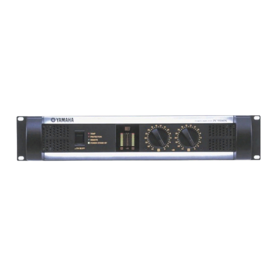
- Page 4 MODE スイッチ:STEREO/BRIDGE/PARALLEL HPF スイッチ:ON/OFF(チャンネル単位) fc = 40Hz DIP スイッチ(6P) コネクター INPUT XLR-3-31 タイプ ユーロブロックコネクター(バランス) (チャンネル単位) OUTPUT スピコン(チャンネル単位) 、5 ウェイバインディング・ポスト NETWORK RJ45 POWER AC インレット(PC4800N) インジケーター POWER/STAND-BY 緑/オレンジ PROTECTION 赤 TEMP 赤(ヒ−トシンク温度≧ 85℃) REMOTE 緑 レベルメーター 10 ポイント LED メーター ロードプロテクション...
- Page 5 XLR 入力端子 MODE switch MODE スイッチ HPF 40 switches HPF 40 スイッチ SPEAKERS 端子 SPEAKERS jacks DATA ポート DATA ports AMP ID スイッチ AMP ID switch ユーロブロックコネクター Euroblock connector AC インレット(PC4800N ) AC inlet (only PC4800N) GND 端子 GND terminals...
- Page 6 PC9500N/PC4800N (ブロックダイアグラム) BLOCK DIAGRAM IN 2/5 IN 1/5 LD704 CN701-11P IC402-1/2 IC402-2/2 JK401 INPUT A ATT IC401 A ATT CN601-11P VR401 RY403-1/2 CN402-35P IC408 1/2 CN401-35P SW402-1/2 IC406 JK403 IN 3/5 RY401 SW401 IN 5/5 -2/4 -3/4 -4/4 CN401-35P CN402-35P...
- Page 7 PC9500N/PC4800N IN 2/5 LD701 +B -B GND CN701-11P CN205-2P CN609-2P CN601-11P CN403 CN201-3P CN605 IC201 CN202 Q420 CN603-6P A ch CN202-6P SP602 W401 CN603-6P SP601 +B -B GND CN205-2P SP603 B ch CN404 CN201-3P IC201 Q418 CN202 CN202-6P CN601-11P CN604-6P...
- Page 8 PC9500N/PC4800N (基板結線図) WIRING B ch PC4800N only...
- Page 9 PC9500N/PC4800N A ch 00N only 38C99-8823966...
- Page 10 PC9500N/PC4800N (寸法図) DIMENSIONS 25 30 30 25 Units: mm (単位)...
- Page 11 PC9500N/PC4800N (分解手順) DISASSEMBLY PROCEDURE トップカバー(所要時間:約 2 分) Top Cover (Time required: about 2 minutes) Remove the nine (9) screws marked [260]. The top [260]のネジ 9 本を外し、トップカバーを外します。 cover can then be removed. (Fig. 1) (Fig.1) リア Ass’y(所要時間:約 4 分) Rear Assembly (Time required: about 4 minutes) トップカバーを外します。...
- Page 12 PC9500N/PC4800N IN 1/5 Circuit Board (Time required: about 5 minutes) IN 1/5 シート(所要時間:約 5 分) Remove the top cover. (See Procedure 1.) トップカバーを外します。 (1 項参照) Remove the rear assembly. (See Procedure 2.) リア Ass’ y を外します。 (2 項参照) Remove the two (2) screws marked [R310] and then [R310]のネジ2本を外し、...
- Page 13 PC9500N/PC4800N [200] [190b] [190a] Side Cover R Side Cover L (サイドカバーR) (サイドカバーL) [170] [170] [170]: Bonding Tapping Screw-B 4.0X8 MFZN2BL (VR779900) ボンディングBタイト [190]: Bonding Tapping Screw-B 4.0X8 MFZN2BL (VR779900) ボンディングBタイト [200]: Bind Head Screw 3.0X4 MFZN2BL (VR139400) +バインド小ネジ Fig.4 DC ファン(所要時間:約 4 分)...
- Page 14 ネジ[P70] (PC9500N:33 本、PC4800N:25 本)と diode marked [P70] (33 screws for PC9500N, 25 [P76]のネジ 3 本、 [P40]のネジ 6 本を外し、PA シー screws for PC4800N), three (3) screws marked [P76] トを外します。 (Fig.7) and six (6) screws marked [P40]. The PA circuit board can then be removed. (Fig. 8)
- Page 15 PC9500N/PC4800N PA5: not installed PA5: not installed [P76] [P70] [P70] [P40] [P40] [P40] PA5: not installed PA5: not installed [P76] [P70] [P70] [P40]: Bind Head Screw 3.0X6 MFZN2BL (EG330360) +バインド小ネジ +バインド小ネジ [P70]: Bind Head Screw-SP 3.0X12 MFZN2Y (VB763800) +バインド小ネジ...
- Page 16 PC9500N/PC4800N (LSI 端子機能表) LSI PIN DESCRIPTION PC9500N IN10: IC801 HD6437042AF28 (X2263100) CPU PC4800N IN5: IC801 NAME FUNCTION NAME FUNCTION TIOC4/DACK0/PE14 MTU I/O / DMA acknowledge / Port E PE15 Port E Data bus Ground Ground Data bus Power supply Address bus...
- Page 17 PC9500N/PC4800N (IC ブロック図) IC BLOCK DIAGRAM TC7W14FU XN883A00 DS36276M (X2155A00) NJM4558M(T1) (IG103520) ● ● PC9500M IN10: IC601, IC602, IC603, PC9500M IN10: IC804 PC9500M IN10: IC802 IC604, IC605, IC606 PC4800M IN5: IC804 PC4800M IN5: IC802 INVERTER TRANSCEIVER PC4800M IN5: IC601, IC602, IC603,...
- Page 18 PC9500N/PC4800N IR2110 (X2382A00) ● PC9500M PS10: IC103,IC104 PC4800M PS5: IC103,IC104 DRIVER DETECT LEVEL PULSE SHIFT FILTER LEVEL SHIFT PULSE PULSE DETECT LEVEL SHIFT DELAY LB1409M (X0654A00) ● PC9500M IN10: IC701, IC702 PC4800M IN5: IC701, IC702 LED DRIVE 13, 12, 11, 10, 9, 8 R7(2.34K), R6(1.66K), R5(1.17K)
- Page 19 PC9500N/PC4800N (シート基板図) CIRCUIT BOARDS CONTENTS (目次) IN 1/5 Circuit Board (X2073C0) ............. 20 IN 2/5 Circuit Board (X2073C0) ............. 22 IN 3/5 Circuit Board (X2073C0) ............. 22 IN 4/5 Circuit Board (X2073C0) ............. 23 IN 5/5 Circuit Board (X2073C0) ............. 23 PA Circuit Board (X2074C0) ............
- Page 20 PC9500N/PC4800N IN 1/5 Circuit Board (PC9500N: IN10, PC4800N: IN5) SPEAKERS OUTPUT from PS-W102 from PS-W103 from PA BCH-W204 from PA ACH-CN205 from PA ACH-W204 from PA ACH-CN205 CN603: to PA ACH-CN202 CN604: to CN601: to IN 2/5-CN701 CN602: f IN: 3NA-V848170...
- Page 21 PC9500N/PC4800N PA BCH-W204 ACH-CN205 from PA ACH-CN201 from PA BCH-CN201 CN402: to IN 5/5-CN401 CN406: to IN 3/5-CN407 ACH-CN202 CN604: to PA BCH-CN202 CN405: to IN 4/5-CN801 to IN 2/5-CN701 CN602: from PS-CN102 (部品側) Component side Pattern side (パターン側) IN: 3NA-V848170...
- Page 22 PC9500N/PC4800N IN 2/5 Circuit Board CN701: to IN 1/5-CN601 (部品側) Component side Pattern side (パターン側) IN 3/5 Circuit Board CN407: to IN 1/5-CN406 Pattern side (パターン側) (部品側) Component side IN: 3NA-V848170...
- Page 23 PC9500N/PC4800N IN 4/5 Circuit Board IN 5/5 Circuit Board CHANNEL INPUT CN801: to IN 1/5-CN405 HPF 40Hz BRIDGE from IN 1/5-CN402 (部品側) Component side AMP ID DATA PORT (部品側) Component side Pattern side (パターン側) Pattern side (パターン側) IN: 3NA-B848170...
- Page 24 PC9500N/PC4800N PA Circuit Board (PC9500N: PA10, PC4800N: PA5) PA ACH: from IN 1/5-CN603 PA BCH: from IN 1/5-CN604 Q235N Q236N Q237N Q238N Q239N Q240N Q241N Q234N Q221N PA ACH: from IN 1/5 -CN609 PA BCH: from IN1/5 -CN610 PA ACH:...
- Page 25 PC9500N/PC4800N Following semi-conductors are installed for the PA unit. (下記半導体はPAユニットで取付さ PA ACH: to PS-CN105 れます。) PA BCH: to PS-CN108 Circuit board ref. Q242N Q243N Q243N Q244N Q245N Q228 Q230 Q232 D241 PA10 D242 ○ ○ Q233 ○ Q231 ○ ○...
- Page 26 to IN 1/5-CN606 from PA ACH-W201 from PA ACH-W202 from PA ACH-W203 AC IN to IN10 1/5 -CN602 from FAN ACH from FAN BCH POWER ON/OFF from PA BCH-W203 from PA BCH-W201 to IN10 1/5-CN607 from PA BCH-W202...
- Page 28 to IN5 1/5-CN606 from PA ACH-W202 from PA ACH-W201 from PA ACH-W203 AC IN to IN5 1/5 -CN602 from FAN ACH from FAN BCH POWER ON/OFF from PA BCH-W203 from PA BCH-W201 from PA BCH-W202 to IN5 1/5-CN607...
- Page 30 PC9500N/PC4800N INSPECTIONS 1. Inspections in STEREO mode and PARALLEL mode 1.1 Preparation Input attenuator Input terminal XLR-3-31 type connector No.2: hot No.1,3: ground MODE SW STEREO Output terminal Unless otherwise specified, load resistance: 8Ω, Non-inductive resistance, power capacity: 1kW or more...
- Page 31 PC9500N/PC4800N 1.2.8 Channel separation Feed the sine wave as specified below to the input terminal of one channel and measure the output voltage. Also, measure the output voltage at the other channel grounded via a 600Ω resistance and check that the voltage measured here is less than - 70dB as compared with the above measured voltage (0dB).
- Page 32 2.3.2 REMOTE, MODEL ID check Using the keyboard of Windows PC, press the return key once and check that REMOTE LED lights up. The monitor screen appears as shown below (for PC4800N). MODEL ID: 0 (PC9500N), MODEL ID: 1 (PC4800N) MODEL ID : 1(PC4800N)
- Page 33 PC9500N/PC4800N 2.3.3 Automatic inspection 2.3.3.1 TEST 10 (STANDBY, PROTECT) Using the keyboard of Windows PC, enter 00 and check that PROTECTION LED lights up and POWER LED lights in orange. (POWER LED lights in orange for about 2 seconds and then changes to green.) The monitor screen appears as shown below and judgment is made automatically.
- Page 34 PC9500N/PC4800N 2.3.3.5 TEST 50 (MUTE) The monitor screen appears as shown below and judgment is made automatically. >>50:MUTE TEST MUTE ON VSP(CH A): 0.00V--<OK> VSP(CH B): 0.00V--<OK> ------------------<TEST50:K> When the TEST 50 result is OK, “——————<TEST 50:OK>” appears on the screen.
- Page 35 PC9500N/PC4800N 2.3.3.8 TEST 80 (MONITOR) The monitor screen appears as shown below and judgment is made automatically. >> 80:MONITOR TEST TEMP(CH A):29C--<OK> TEMP(CH B):28C--<OK> Vpre(CH A):0.67V--<OK> Vpre(CH B):0.65V--<OK> VSP(CH A):29.95V--<OK> VSP(CH B):30.28V--<OK> ISP(CH A):3.37A--<OK> ISP(CH B):3.30A--<OK> ------------------<TEST80:OK> When the TEST 80 result is OK, “—————<TEST 80:END>” appears on the screen.
- Page 36 PC9500N/PC4800N BRIDGE mode 3.1 Preparation Input attenuator Operation for Ach only. MAX. Input terminal XLR-3-31 type MODE switch BRIDGE Output terminal Ach + and Bch+ used. DATA port Unused AMP ID switch 1,2,4,8,16,T OFF Load resistor 8Ω+8Ω non-inductive resistance, power capacity 1kW or more Connection of measuring instrument Connect to the mid-point of load resistor with the ground floated.
- Page 37 PC9500N/PC4800N 検査 STEREO モード、PARALLEL モード時の検査 1.1 準備 入力アッテネーター 入力端子 XLR-3-31 type 2 番ホット 1,3 番アース MODE SW STEREO 出力端子 指定のない場合は、負荷抵抗 8 Ω 無誘導抵抗 電力容量 1KW 以上 DATA PORT 使用しない。 AMP ID SW 1, 2, 4, 8, 16, T OFF その他 指定のない場合は、両 ch 駆動とする。...
- Page 38 PC9500N/PC4800N 1.2.9 出力ノイズレベル 入力アッテネーターを MAX、入力端子を、600Ω の抵抗を介して接地し、出力端子に発生するノイズレベルを測定し、-65dB 以下であることを確認します。次に入力アッテネーターを MIN にし、ノイズレベルは -70dB 以下であることを確認します。 1.2.10 安定度 10kHz、-10dB の、矩形波を入力し、負荷抵抗 4Ω に並列に 10pF ∼ 0.47uF の容量を接続した時、以下の項目を満足することを 確認します。 オーバーシュート : Vp/Vo ≦ 1.8 リンギング : 5 波以内 次に、負荷を純容量 10pF ∼ 0.47uF のみとした時 Vp/Vo ≦ 2.5 リンギングは、7 波以内にて収束し、発振などを生じないことを確認します。...
- Page 39 <<<<< PC-N Series Amplifier Test Program >>>> - FIRMWARE VERSION: V*.** - TEST PROGRAM VERSION: V*.** *.**: バージョン番号 2.3.2 REMOTE、MODEL ID 検査 Windows PC のキーボードよりリターンを1回入力します。REMOTE LED が点灯することを確認します。 そのときモニタ画面が次の文字を表示します。 (下記は PC4800N の場合です。 ) MODEL ID : 0(PC9500N) 、MODEL ID : 1(PC4800N) MODEL ID : 1(PC4800N)
- Page 40 PC9500N/PC4800N 2.3.3 自動検査 2.3.3.1 TEST 10 検査(STANDBY,PROTECT) Windows PC のキーボードより 00 の文字を入力します。 (半角文字) PROTECTION LED が点灯し、POWER LED が橙色に点灯します。 (POWER LED は約 2sec の間、橙色に点灯します。その後、緑色に変わります。 ) モニタ画面が次の文字を表示し、自動で判定を行います。 >>00:ALL TEST >>10:POWER TEST Waiting for PROTECTION=NONE... PROTECTION :NONE--<OK> POWER:STANDBY Wait 2sec.. PROTECTION :ON--<OK> POWER:ON ------------------<TEST10:OK> TEST10 が OK の場合は...
- Page 41 PC9500N/PC4800N 2.3.3.4 TEST 40 検査(ATT) モニタ画面が次の文字を表示し、自動で判定を行います。 >>40:ATT TEST ATT=-6dB VSP(CH A):14.64V--<OK> VSP(CH B):14.75V--<OK> ------------------<TEST40:OK> TEST40 が OK の場合は ------------------<TEST40:OK> が表示されます。 TEST40 終了後自動で TEST50 に進みます。 2.3.3.5 TEST 50(MUTE) モニタ画面が次の文字を表示し、自動で判定を行います。 >>50:MUTE TEST MUTE ON VSP(CH A): 0.00V--<OK> VSP(CH B): 0.00V--<OK> ------------------<TEST50:K> TEST50 が OK の場合は...
- Page 42 PC9500N/PC4800N TEST70 が OK の場合は ------------------<TEST70:END> が表示されます。 TEST70 終了後自動で TEST80 に進みます。 2.3.3.8 TEST 80(MONITOR) モニタ画面が次の文字を表示し、自動で判定を行います。 >> 80:MONITOR TEST TEMP(CH A):29C--<OK> TEMP(CH B):28C--<OK> Vpre(CH A):0.67V--<OK> Vpre(CH B):0.65V--<OK> VSP(CH A):29.95V--<OK> VSP(CH B):30.28V--<OK> ISP(CH A):3.37A--<OK> ISP(CH B):3.30A--<OK> ------------------<TEST80:OK> TEST80 が OK の場合は ------------------<TEST80:OK> が表示されます。...
- Page 43 PC9500N/PC4800N BRIDGE モード 3.1 準備 入力アッテネーター A ch のみ作動。MAX。 入力端子 A ch XLR-3-31 type(2 番ホット、13 番ホット) MODE SW BRIDGE 出力端子 Ach +、Bch + を使用。 DATA PORT 使用しない。 AMP ID SW 1, 2, 4, 8, 16, T OFF 負荷抵抗 8 Ω + 8 Ω 無誘導抵抗、電力容量 1kW 以上...
- Page 44 OVERALL CIRCUIT DIAGRAMS (目次) CONTENTS PC9500N/PC4800N OVERALL CIRCUIT DIAGRAM 1/8 (IN 1/5, IN 3/5, IN 5/5) ... C1 PC9500N/PC4800N OVERALL CIRCUIT DIAGRAM 2/8 (IN 1/5) ......C2 PC9500N/PC4800N OVERALL CIRCUIT DIAGRAM 3/8 (IN 2/5) ......C3 PC9500N/PC4800N OVERALL CIRCUIT DIAGRAM 4/8 (IN 1/5) ......C4 PC9500N/PC4800N OVERALL CIRCUIT DIAGRAM 5/8 (IN 4/5) ......
- Page 45 PC9500N/PC4800N PC9500N/PC4800N OVERALL CIRCUIT DIAGRAM 1/8 (IN 1/5, IN 3/5, IN 5/5) from IN10 1/5 M5 (P.C2) IN 1/5 from IN 1/5 J10 (P.C2) from IN 1/5 B8 (P.C2) from IN 1/5 B7 (P.C2) from IN 1/5 A2 (P.C1) from IN 1/5 N8 (P.C2)
- Page 46 PC9500N/PC4800N OVERALL CIRCUIT DIAGRAM 2/8 (IN 1/5) PC9500N/PC4800N IN 1/5 to IN 1/5 F2 (P.C4) to IN 1/5 F4 (P.C4) from PA Ach-CN205 to IN 1/5 C1 (P.C4) to IN 1/5 P2 OP AMP (P.C1) OP AMP to IN10 1/5 (P.C4) from PA Bch-CN205 to IN 1/5 P1 (P.C1)
- Page 47 PC9500N/PC4800N PC9500N/PC4800N OVERALL CIRCUIT DIAGRAM 3/8 (IN 2/5) IN 2/5 LED DRIVER LED DRIVER to IN 1/5 TP749 -CN601 TP748 UDZS-13B : Ceramic Capacitor ( セラコン ) 2 . 2 k Note : See parts list for details of circuit board component parts.
- Page 48 PC9500N/PC4800N OVERALL CIRCUIT DIAGRAM 4/8 (IN 1/5) PC9500N/PC4800N from IN 2/5 F2 (P.C2) IN 1/5 to IN 1/5 D8 (P.C1) from IN 1/5 D8 (P.C1) to IN 1/5 D8 (P.C1) to IN 1/5 H8 (P.C1) from IN 1/5 K1 (P.C2)
- Page 49 PC9500N/PC4800N PC9500N/PC4800N OVERALL CIRCUIT DIAGRAM 5/8 (IN 4/5) IN 4/5 SYSTEM RESET INVERTER from IN 1/5-CN405 AMP ID DATA PORT 3NA-V848170 Note : See parts list for details of circuit board component parts. 注 : シートの部品詳細はパーツリストをご参照下さい。 PC9500N/PC4800N PC9500N/PC4800N...
- Page 50 PC9500N/PC4800N OVERALL CIRCUIT DIAGRAM 6/8 (PA) PC9500N/PC4800N N.C. OFFSET ADJUST MENT PA Ach: from IN1/5-CN403 PA Ach: to PS-CN105 PA Bch: from IN1/5-CN404 PA Bch: to PS-CN108 PA Ach: to PS-CN106 PA Bch: to PS-CN109 PA Ach: to PS-CN107 PA Ach: from IN 1/5-CN609...
- Page 51 PC9500N/PC4800N PC9500N/PC4800N OVERALL CIRCUIT DIAGRAM 7/8 (PS10) REGULATOR +5V REGULATOR +15V AC IN NJM7815FA (XD853A00) REGULATOR +15V NJM7805FA (XJ607A00) REGULATOR +5V 1: INPUT 2: GND 3: OUTPUT NJM7915FA (XD854A00) REGULATOR -15V REGULATOR +15V 1: OUTPUT from PA Ach 2: COMMON...
- Page 52 PC9500N/PC4800N OVERALL CIRCUIT DIAGRAM 8/8 (PS5) PC9500N/PC4800N REGULATOR +5V REGULATOR +15V Power Switch POWER TRANSFORMER AC cord from PA Ach-W201 from PA Ach-W202 from PA Ach-W203 from PA Bch-W201 from PA Bch-W202 from PA Bch-W203 REGULATOR +15V to IN5-CN602 REGULATOR -15V...
- Page 53 (総組立) OVERALL ASSEMBLY ..........2 (PC9500N電気部品) ELECTRICAL PARTS PC9500N ....6 (PC4800N電気部品) ELECTRICAL PARTS PC4800N .... 21 Notes : DESTINATION ABBREVIATIONS A : Australian model M : South African model B : British model O : Chinese model C : Canadian model...
- Page 54 PC9500N/PC4800N (総組立) OVERALL ASSEMBLY Rear Assembly (リアAss'y) (J) model is not installed. R20a R20e PA Unit (PAユニット) 30 2/2 R20b R20c J model 30 1/2 F140 F130 R20d F190 F120 F110 F140 F180 F160 F150 F130 F100 F170 F120 F180 Front Assembly (フロントAss'y)...
- Page 55 総 組 立 PC9500N A (V853290) Overall Assembly 総 組 立 PC9500N K (V888560) 総 組 立 Overall Assembly PC4800N J (V853300) 総 組 立 Overall Assembly PC4800N U,V (V853310) 総 組 立 Overall Assembly PC4800N H,W (V853320) 総 組...
- Page 56 PC9500N/4800N V 8 2 4 6 3 0 0 AC Cord J VCTF 2.0X3 電 源 コ ー ド PC4800N J V 8 2 4 6 4 0 0 AC Cord UC SJT 14AWGX3 電 源 コ ー ド V 8 2 4 6 5 0 0 AC Cord E H05VV-F 3X1.00...
- Page 57 PC9500N/PC4800N PART NO. DESCRIPTION 部 品 名 REMARKS REF NO. RANK + バ イ ン ド B タ イ ト VB096700 Bind Head Tapping Screw-B 2.6X8 MFZN2BL V 9 5 6 8 8 0 0 Flat Fillister H.Tapping 3.0X8 MFZN2BL +...
- Page 58 PC9500N (PC9500N 電気部品) ELECTRICAL PARTS PC9500N PART NO. DESCRIPTION 部 品 名 REMARKS REF NO. RANK 電 気 部 品 ELECTRICAL PARTS PC9500N シ ー ト I N 1 0 Circuit Board IN10 (V848170,X2073C0) AAX34690 Circuit Board IN10 1/5 シ...
- Page 59 PC9500N PART NO. DESCRIPTION 部 品 名 REMARKS REF NO. RANK チ ッ プ セ ラ C623 UX064100 Ceramic Capacitor (Chip) 0.0100 50V K -627 UX064100 Ceramic Capacitor (Chip) 0.0100 50V K チ ッ プ セ ラ C628 UR848100 Electrolytic Cap. 100.00 25.0V ケ...
- Page 60 PC9500N PART NO. DESCRIPTION 部 品 名 REMARKS REF NO. RANK コ ネ ク タ ベ ー ス ポ ス ト CN602 VV066900 Connector Base Post M2426XX 9P TE CN603 VV066600 Connector Base Post M2426XX 6P TE コ ネ ク タ ベ ー ス ポ ス ト CN604 VV066600 Connector Base Post...
- Page 61 PC9500N PART NO. DESCRIPTION 部 品 名 REMARKS REF NO. RANK デ ジ タ ル ト ラ ン ジ ス タ -413 VV655000 Digital Transistor DTA114EKA TP Q414 VV655400 Digital Transistor DTC114EKA TP デ ジ タ ル ト ラ ン ジ ス タ -416 VV655400 Digital Transistor...
- Page 62 PC9500N PART NO. DESCRIPTION 部 品 名 REMARKS REF NO. RANK チ ッ プ 抵 抗 R423 RG007220 Carbon Resistor (chip) 22K 0.1 J R424 V I 1 9 7 8 0 0 Metal Film Resistor(chip) 15.0K 1/10 D チ ッ プ 金 被 抵 抗 R425 V I 1 9 7 8 0 0 Metal Film Resistor(chip)
- Page 63 PC9500N PART NO. DESCRIPTION 部 品 名 REMARKS REF NO. RANK チ ッ プ 抵 抗 R615 RF356430 Carbon Resistor (chip) 4.3K D 1608 R616 RF357360 Carbon Resistor (chip) 36.0K D 1608 チ ッ プ 抵 抗 R617 RF357470 Carbon Resistor (chip) 47.0K D 1608 チ...
- Page 64 PC9500N PART NO. DESCRIPTION 部 品 名 REMARKS REF NO. RANK チ ッ プ 抵 抗 R717 RG007220 Carbon Resistor (chip) 22K 0.1 J R718 RG007220 Carbon Resistor (chip) 22K 0.1 J チ ッ プ 抵 抗 R720 RG007100 Carbon Resistor (chip) 10K 0.1 J チ...
- Page 65 PC9500N PART NO. DESCRIPTION 部 品 名 REMARKS REF NO. RANK チ ッ プ 抵 抗 R923 RF357470 Carbon Resistor (chip) 47.0K D 1608 チ ッ プ 抵 抗 -930 RF357470 Carbon Resistor (chip) 47.0K D 1608 R931 RG007100 Carbon Resistor (chip) 10K 0.1 J チ...
- Page 66 PC9500N PART NO. DESCRIPTION 部 品 名 REMARKS REF NO. RANK マ イ ラ ー コ ン C233 V 2 3 4 7 4 0 0 Mylar Capacitor 7500P 50V J C234 V 3 2 8 0 5 0 0 Ceramic Capacitor-B 100P 500 K セ...
- Page 67 PC9500N PART NO. DESCRIPTION 部 品 名 REMARKS REF NO. RANK カ ー ボ ン 抵 抗 R205 HF458330 Carbon Resistor 330.0K 1/4 J R206 HF455560 Carbon Resistor 560.0 1/4 J カ ー ボ ン 抵 抗 R207 HF457100 Carbon Resistor 10.0K 1/4 J カ...
- Page 68 PC9500N PART NO. DESCRIPTION 部 品 名 REMARKS REF NO. RANK 不 燃 化 カ ー ボ ン 抵 抗 R306 VZ008800 Flame Proof C. Resistor 22.0 1/4 J 不 燃 化 カ ー ボ ン 抵 抗 R307 VZ008700 Flame Proof C.
- Page 69 PC9500N PART NO. DESCRIPTION 部 品 名 REMARKS REF NO. RANK マ イ ラ ー コ ン C104 UA952470 Mylar Capacitor 470P 50V J ケ ミ コ ン C105 UR857100 Electrolytic Cap. 10.00 35.0V C106 UA952470 Mylar Capacitor 470P 50V J マ...
- Page 70 PC9500N PART NO. DESCRIPTION 部 品 名 REMARKS REF NO. RANK ダ イ オ ー ド D109 V 8 6 2 9 7 0 0 Diode RL3A ダ イ オ ー ド -112 V 8 6 2 9 7 0 0 Diode RL3A D113...
- Page 71 PC9500N PART NO. DESCRIPTION 部 品 名 REMARKS REF NO. RANK カ ー ボ ン 抵 抗 R105 HF455560 Carbon Resistor 560.0 1/4 J カ ー ボ ン 抵 抗 R106 HF455560 Carbon Resistor 560.0 1/4 J R107 HF455330 Carbon Resistor 330.0 1/4 J カ...
- Page 72 PC9500N PART NO. DESCRIPTION 部 品 名 REMARKS REF NO. RANK 電 源 ト ラ ン ス T104 X2392A00 Power Transformer 電 源 ト ラ ン ス T104 X2393A00 Power Transformer U,V,A T104 X2394A00 Power Transformer 電 源 ト ラ ン...
- Page 73 PC4800N (PC4800N 電気部品) ELECTRICAL PARTS PC4800N PART NO. DESCRIPTION 部 品 名 REMARKS REF NO. RANK 電 気 部 品 ELECTRICAL PARTS PC4800N シ ー ト I N 5 1 / 5 AAX39260 Circuit Board IN5 1/5 (X2073C0)
- Page 74 PC4800N PART NO. DESCRIPTION 部 品 名 REMARKS REF NO. RANK チ ッ プ セ ラ -627 UX064100 Ceramic Capacitor (Chip) 0.0100 50V K C628 UR848100 Electrolytic Cap. 100.00 25.0V ケ ミ コ ン C629 UR848100 Electrolytic Cap. 100.00 25.0V ケ...
- Page 75 PC4800N PART NO. DESCRIPTION 部 品 名 REMARKS REF NO. RANK コ ネ ク タ ベ ー ス ポ ス ト CN603 VV066600 Connector Base Post M2426XX 6P TE CN604 VV066600 Connector Base Post M2426XX 6P TE コ ネ ク タ ベ ー ス ポ ス ト...
- Page 76 PC4800N PART NO. DESCRIPTION 部 品 名 REMARKS REF NO. RANK デ ジ タ ル ト ラ ン ジ ス タ Q414 VV655400 Digital Transistor DTC114EKA TP -416 VV655400 Digital Transistor DTC114EKA TP デ ジ タ ル ト ラ ン ジ ス タ...
- Page 77 PC4800N PART NO. DESCRIPTION 部 品 名 REMARKS REF NO. RANK チ ッ プ 金 被 抵 抗 R424 V I 1 9 7 8 0 0 Metal Film Resistor(chip) 15.0K 1/10 D R425 V I 1 9 7 8 0 0 Metal Film Resistor(chip) 15.0K 1/10 D...
- Page 78 PC4800N PART NO. DESCRIPTION 部 品 名 REMARKS REF NO. RANK チ ッ プ 抵 抗 R616 RF357360 Carbon Resistor (chip) 36.0K D 1608 R617 RF357470 Carbon Resistor (chip) 47.0K D 1608 チ ッ プ 抵 抗 R618 VZ008800 Flame Proof C. Resistor 22.0 1/4 J...
- Page 79 PC4800N PART NO. DESCRIPTION 部 品 名 REMARKS REF NO. RANK チ ッ プ 抵 抗 R718 RG007220 Carbon Resistor (chip) 22K 0.1 J R720 RG007100 Carbon Resistor (chip) 10K 0.1 J チ ッ プ 抵 抗 R721 RF357110 Carbon Resistor (chip) 11.0K...
- Page 80 PC4800N PART NO. DESCRIPTION 部 品 名 REMARKS REF NO. RANK チ ッ プ 抵 抗 R931 RG007100 Carbon Resistor (chip) 10K 0.1 J R932 RG007100 Carbon Resistor (chip) 10K 0.1 J チ ッ プ 抵 抗 R933 RF357470 Carbon Resistor (chip) 47.0K...
- Page 81 PC4800N PART NO. DESCRIPTION 部 品 名 REMARKS REF NO. RANK コ ネ ク タ ベ ー ス ポ ス ト CN201 VV066300 Connector Base Post M2426XX 3P TE CN202 VV066600 Connector Base Post M2426XX 6P TE コ ネ ク タ ベ ー ス ポ ス ト...
- Page 82 PC4800N PART NO. DESCRIPTION 部 品 名 REMARKS REF NO. RANK カ ー ボ ン 抵 抗 R208 HF455560 Carbon Resistor 560.0 1/4 J R209 VN688500 Carbon Resistor 12K 1/2 F カ ー ボ ン 抵 抗 R210 VN688500 Carbon Resistor 12K 1/2 F カ...
- Page 83 PC4800N PART NO. DESCRIPTION 部 品 名 REMARKS REF NO. RANK セ メ ン ト 抵 抗 R316 VZ370200 Wire Wound Resistor 0.1 5W K 不 燃 化 カ ー ボ ン 抵 抗 R317 VV557800 Flame Proof C. Resistor 1.0 1/4 J...
- Page 84 PC4800N PART NO. DESCRIPTION 部 品 名 REMARKS REF NO. RANK ケ ミ コ ン C119 V 8 4 9 9 1 0 0 Electrolytic Cap. 2200 200V ケ ミ コ ン C120 V 8 4 9 9 1 0 0 Electrolytic Cap.
- Page 85 PC4800N PART NO. DESCRIPTION 部 品 名 REMARKS REF NO. RANK コ イ ル L101 V 8 9 2 9 3 0 0 Coil SC-10-20JH H,W,B,K,A コ イ ル L102 V 0 0 7 6 3 0 0 Coil H,W,B,K...
- Page 86 PC4800N PART NO. DESCRIPTION 部 品 名 REMARKS REF NO. RANK 電 源 ト ラ ン ス T102 X2388A00 Power Transformer 電 源 ト ラ ン ス T102 X2389A00 Power Transformer T102 X2390A00 Power Transformer 電 源 ト ラ ン...
Need help?
Do you have a question about the PC4800N and is the answer not in the manual?
Questions and answers