Table of Contents
Advertisement
Quick Links
SERVICE MANUAL
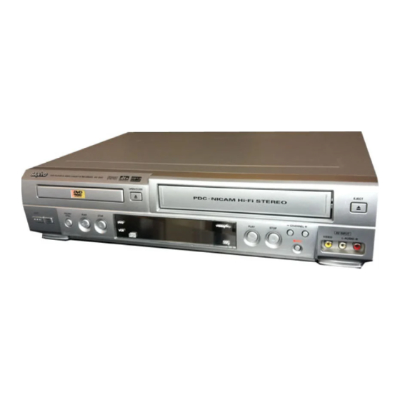
DVD Player + Video Cassette
Recorder
CAUTION
This product utilizes a laser.
The adjustment other than those specified herein may result in hazardous radiation exposure.
KW4HV/E, EV, SP
FILE NO.
HV-DX1E
(Product Code : 143 187 02)
(U.K.)
HV-DX1EV
(Product Code : 143 187 03)
(Europe)
HV-DX1SP
(Product Code : 143 187 04)
(Spain)
PAL
REFERENCE No.SM5310392
Advertisement
Chapters
Table of Contents
Troubleshooting

Related Manuals for Sanyo HV-DX1E


Summary of Contents for Sanyo HV-DX1E
- Page 1 FILE NO. SERVICE MANUAL DVD Player + Video Cassette HV-DX1E Recorder (Product Code : 143 187 02) (U.K.) HV-DX1EV (Product Code : 143 187 03) (Europe) HV-DX1SP (Product Code : 143 187 04) (Spain) CAUTION This product utilizes a laser.
- Page 2 CONTENTS SECTION 1 ..SUMMARY SECTION 2 ..CABINET & MAIN CHASSIS SECTION 3 ..ELECTRICAL SECTION 4 ..MECHANISM OF VCR PART SECTION 5 ..MECHANISM OF DVD PART SECTION 6 .
-
Page 3: Deck Mechanism
MECHANISM TROUBLESHOOTING GUIDE 1.Deck Mechanism Auto REW doesn't work. Is the output of END sensor of supply side "H"? “H”: more than 3.5V “L”: less than 0.7V~1V Is the Vcc. voltage of End Check the syscon power. sensor 5V? Replace End sensor. Is the voltage across IR LED Replace LED. - Page 4 MECHANISM TROUBLESHOOTING GUIDE AUTO STOP. (PLAY/CUE/REV) Check aligment positions (page 4- 14) Check spring Pinch. In Play/Cue/Rev is the pinch roller in contact with the capstan Is the output of DFG, DPG OK? Replace Drum Motor. shaft. Are there T/up and supply reel Check Servo, Syscon.
- Page 5 MECHANISM TROUBLESHOOTING GUIDE In PB mode Tape Presence not sensed. Is the Pinch Roller attached Check Alignment positions to the Capstan Motor Shaft? (page 4-14) Does the T/Up Is the Belt ok? Replace the Belt. Reel turn? Check the clutch and the Idler Does the Capstan Motor turn? Assembly.
-
Page 6: Front Loading Mechanism
MECHANISM TROUBLESHOOTING GUIDE 2. Front Loading Mechanism Cassette cannot be inserted. Does the Lever Assembly Is the Lever Assembly Switch Replace or add the Lever Switch work? Spring damaged or omitted? Assembly Switch Spring. Does the CST IN Switch work Replace CST IN Switch. - Page 7 MECHANISM TROUBLESHOOTING GUIDE Cassette will not load. Does the CST insert? Does the opener Lid work? Replace the Opener Lid. Does the Gear Rack F/L work? Replace the Rear Rack F/L. Does the Opener Door work? Does the Arm Assembly F/L work? Is the opener Door assembled correctly? Does the L/D Motor work? Replace the Arm Assembly F/L.
-
Page 8: Exploded Views
EXPLODED VIEWS 1. Front Loading Mechanism Section 4-28... - Page 9 EXPLODED VIEWS 2. Moving Mechanism Section(1) OPTIONAL PART 4-29...
- Page 10 EXPLODED VIEWS 3. Moving Mechanism Section(2) 4-30...
-
Page 11: Table Of Contents
SECTION 3 ELECTRICAL CONTENTS OVERALL BLOCK DIAGRAM ...........................3-1 VCR PART ELECTRICAL ADJUSTMENT PROCEDURES .......................3-2 ELECTRICAL TROUBLESHOOTING GUIDE ......................3-3 1. POWER(SMPS) CIRCUIT ............................3-3 2. SYSTEM/KEY CIRCUIT ...............................3-7 3. SERVO CIRCUIT................................3-8 4. Y/C CIRCUIT ................................3-11 5. Hi-Fi CIRCUIT ................................3-15 6. Tuner/IF CIRCUIT ..............................3-18 BLOCK DIAGRAMS ..............................3-20 1. - Page 12 OVERALL WIRING DIAGRAM...
-
Page 13: Vcr Part
VCR PART ELECTRICAL ADJUSTMENT PROCEDURES 1. Servo Adjustment 1) PG Adjustment • Test Equipment a) OSCILLOSCOPE C) PAL MODEL : PAL SP TEST TAPE b) NTSC MODEL : NTSC SP TEST TAPE • Adjustment And Specification MODE MEASUREMENT POINT ADJUSTMENT POINT SPECIFICATION V.Out PLAY... -
Page 14: Electrical Troubleshooting Guide
ELECTRICAL TROUBLESHOOTING GUIDE 1. Power(SMPS) CIRCUIT (1) No 5.3VA (SYS/Hi-Fi/TUNER) (2) No 12VA (TO CAP, DRUM MOTOR) NO 5.3VA. NO 12VA. Replace the F101. Is the Vcc(13V) supplied to (+) Check or Replace Is the F101 normal? (Use the same Fuse) terminal in D115 and D117? the D110. - Page 15 (4) No 5V (TO DVD) (5) No REG 5VT (SYS/AVCP/TU/CANAL) NO 5V. No 5.2VT. Is the Q118 Base Is 5.3VA put into Check the Timer 5.3VA Line Check. the Q113 Emitter? control. “H”? Is 5.3VA put into the Is the Q115 Base Check the Power 5.3VA Line Check.
- Page 16 (8) No -27VA (9) No 8VA NO -27VA. NO 8VA. Check or Replace Check or Replace Is Vcc(13V) supplied to D108. (+) terminal in D114? the D110. Check or Replace Is Vcc(12V) supplied to IC106 Pin1? the D114. Check the Power Is the Q115 Base “H”? Control.
-
Page 17: System/Key Circuit
2. SYSTEM/KEY CIRCUIT (1) AUTO STOP Auto Stop Does the SW25 waveform Check the Drum Motor appear at the IC501 signal. Pin105? Do T/UP Reel Pulses Do the T-UP Reel Pulses Does 5.2V appear at the appear at the Q514 appear at the IC501 Pin49? RS501? Base terminal ? -
Page 18: Servo Circuit
3. SERVO CIRCUIT (1) Unstable Video in PB MODE Unstable Video in PB Mode. Does the Noise level of the screen change periodically? Do the CTL pulses appear Is adjusting the height of at the IC501 Pin8? the CTL Head accurate? Does the CFG waveform Readjust the height of the appear at the IC501... - Page 19 2. SERVO CIRCUIT (3) When the Capstan Motor doesn’t run, When the Capstan Motor doesn’t run, Refer to “SMPS(CAPSTAN/12Volt) Does 12VA appear at the PMC01? Trouble Shooting”. Does 2.8V appear at the PMC01? Check the PMC01 and the Capstan Does the PWM signal appear at the Motor Ass’y.
- Page 20 (4) KEY doesn’t working KEY doesn’t working. Is 5V applied to the IC501 Refer to “SMPS 5.3VA Pin36? Trouble Shooting”. Does LED or FLD change Replace the defective when a function button is switches. pressed?
-
Page 21: Y/C Circuit
4. Y/C CIRCUIT (1) No Video in EE Mode, No Video in EE Mode Does the Video signal Check the 24Pin of Tuner. appear at the IC301 Pin48? Is 5V applied to the IC301 Check the 5.2VT, 5.3VA Pins18, 24, 42, 55, 72, 91? Line. - Page 22 3. Y/C CIRCUIT (2) When the Y(Luminance) signal doesn’t appear on the screen in PB Mode, Is 5.2VT, 5.3VA applied to the Check the line of the 5.2VT, 5.3VA Line. (Power Circuit) IC301 Pins24, 42, 55, 72, 91? Is the I C Bus siganl applied Refer to ‘SYSTEM I C BUS...
- Page 23 3. Y/C CIRCUIT (3) When the C(Color) signal doesn’t appear on the screen in PB Mode, Is 5.2VT/5.3VA applied to the Check the line of the 5.2VT/ 5.3VA Line. (Power Circuit) IC301 Pins24, 42, 55, 72, 91. Is the Color Rotary signal Check the Color Rotary applied to the IC301 Circuit.
- Page 24 3. Y/C CIRCUIT (4) When the Video signal doesn’t appear on the screen in REC Mode, Is the EE signal normal? Check EE Mode. Is 5.2VT/5.3VA applied to the Check the line of the 5.2VT/ IC301 Pins24,42,55,72,91? 5.3VA Line.(Power Circuit) Does PB Mdoe operate Check PB Mode.
-
Page 25: Hi-Fi Circuit
5. Hi-Fi CIRCUIT (A) No Sound(EE Mode) No Sound. Check the TU Audio of IC801 Check the IC751 Pins30, 31. Pins1, 3. Check the DVD Audio of IC801 Check the DVD MODULE. (P8D01 Pins3, 5). Pins4, 5. Check the AV1 Audio of IC801 Check the Scart1 Jack. - Page 26 3. Y/C CIRCUIT (B) Hi-Fi Playback PB mode No Sound. Check the Vcc of IC801 Check Power 5.2V, 12VT. (Pins34, 40) Check the Hi-Fi Selection switch. Check IC501 Pin25 (IC801 Pin41) and the Tape quality. (A.H/SW) Is the RF Envelope at IC801 Pin44 over 2Vp-p? Check IC801 Pin42(Data), Check the parts of µ-COM...
- Page 27 Hi-Fi REC. It is impossible to record Hi-Fi Audio signal. Check Vcc of IC801.(Pins34, 40) Check Power 5V, 12VT. Check IC801 Pin42(Data), Pin43(CLOCK). Check ports of µ-COM. Check Audio input signal of IC801 Do Audio signals appear at IC801 Pins2, 3(TU.A.), 4, 5(DVD.A.), Pins16, 17? 6, 7(AVI.A.), 8, 9(AV2.A.), 10, 11(AV3.A.).
-
Page 28: Tuner/If Circuit
6. Tuner/IF CIRCUIT (A) No Picture on the TV screen No picture on the TV screen Does the Video signal at Is +33V applied to TU701 Check 33V line. the TU701 Pin24. Pin16? Is +5V applied to TU701 Check 5V line. Pin13? Does the Clock signal Check the lIC Clock Signal... - Page 29 (B) No Sound No Sound. Check the Vcc of IC751 Pins1, 11, 19, Check 5.2V Line. 22, 33. Check the Tuner SiF signal at IC751 Check the Tuner SIF of TU701 Pin22. Pin2. Check the oscillator of IC751 Pins5, 6. Replace X751 Check the IIC Clock and Data at IC751 Check the Audio of IC751 Pins30, 31.
- Page 30 MEMO 3-19...
-
Page 31: Power(Smps) Circuit Diagram
2. Voltages are DC-measured with a digital voltmeter MODIFIED OR ALTERED WITHOUT PERMISSION IMPLEMENTATION OF THE LATEST SAFETY AND during Play mode. FROM THE SANYO ELECTRONICS CORPORATION. PERFORMANCE IMPROVEMENT CHANGES INTO ALL COMPONENTS SHOULD BE REPLACED ONLY THE SET IS NOT DELAYED UNTIL THE NEW SERVICE WITH TYPES IDENTICAL TO THOSE IN THE ORIGI- LITERATURE IS PRINTED. - Page 32 2. TU/IF, NICAM & A2 CIRCUIT DIAGRAM SANYO SCART EE MODE(VIDEO) TU MODE (AUDIO) 3-32 3-33...
- Page 33 No mono Audio Signal FL301, Q301, Q306 are defective. in PB MODE. Normal Audio signal is not recorded. PB Y+C REC Y+C REC AUDIO SANYO SCART PB Y REC Y PB AUDIO(MONO) PB C REC C WAVEFORM 3-34...
-
Page 34: Hi-Fi Circuit Diagram
4. Hi-Fi CIRCUIT DIAGRAM IC801 Pins42, 43 aredefective. All Audio is not appear. 44 Pin is defective. Hi-Fi Audio is not appear. HV-DX1UK CANAL(DX1EV,SP) 2_SCART(DX1UK) SANYO SCART 3-36 3-37... -
Page 35: Scart(Jack) Circuit Diagram
5. SCART(JACK) CIRCUIT DIAGRAM (DX1UK) (DX1EV,SP) SANYO SCART 3-38 3-39... -
Page 36: System Circuit Diagram
R578 are defective. VCR will not operate. IC505 is defective. ALL MODELS Auto stop occures. Auto Rew will not working. RS501,RS502,Q514, SANYO SCART Q515 are defective. ES501, ES502, LD501 are defective. µ-COM is unstable. Q501, Q503 are defective. WAVEFORM 3-40... - Page 37 WAVEFORM & VOLTAGE SHEET _ C301 Osc oscope Wave orm * C501 Waveform Photographs @ @ @ @ @ @ @ @ @ @ h e ? @ @ ? h e ? @ @ @ @ @ @ @ @ @ @ @ @ @ @ @ @ @ @ @ @ @ @ @ @ @ @ @ @ @ @ @ @ @ @ @ @ @ @ @ @ @ @ @ @ @ @ @ @ @ @ @ @ @ h e ? @ @ ? h e ? @ ( M e ? I ' @ @ @ e @ @ @ @ @ @ @ @ @ @ @ @ @ @ @ @ @ @ @ @ @ @ @ @ @ @ @ @ @ @ g ? @ @ @ @ @ @ @ h e W 2 @ 6 X ? f W 2 @ 6 X ? e ? @ @ @ f ? @ @ @ e ? W 2 @ @ @ 6 X g ? @ @ ? @ @ f ? W 2 @ @ 6 X ? e ? @ @ ? ? W 2 @ g ? @ H ? W 2 6 K V @ @ 5 e @ @ @ @ @ @ @ @ @ @ @ @ @ @ @ @ @ @ @ @ @ @ @ @ @ @ @ @ @ @ g ? @ @ @ @ @ @ @ h ? W &...
-
Page 38: Circuit Voltage Chart
• CIRCUIT VOLTAGE CHART MODE MODE MODE MODE MODE MODE MODE PIN NO. PIN NO. PIN NO. PIN NO. PIN NO. PIN NO. PIN NO. I C 3 0 1 4.52 3.58 pulse pulse pulse pulse pulse pulse pulse 0.26 4.57 0.27 pulse... - Page 39 Tran- EE Mode PB Mode REC Mode sistor Q110 -21.8 -21.8 Q111 5.23 5.24 5.23 Q112 12.1 13.9 12.7 13.5 12.7 12.1 13.4 12.7 Q113 5.24 5.18 4.46 5.24 5.18 4.46 5.24 5.17 4.47 Q114 33.6 33.5 32.8 33.4 33.2 32.4 33.5 33.3...
-
Page 40: Printed Circuit Diagrams
PRINTED CIRCUIT DIAGRAMS 1. MAIN P.C.BOARD NOTES) Warning NOTES) Parts that are shaded are critical NOTES) With respect to risk of fire or NOTES) electricial shock. LOCATION GUIDE 3-48 3-49... -
Page 41: Key P.c.board
2. KEY P.C.BOARD LOCATION GUIDE LOCATION GUIDE 3. CLOCK P.C.BOARD 3-50 3-51... -
Page 42: Dvd Part
DVD PART ELECTRICAL TROUBLESHOOTING GUIDE 1. µ-COM Circuit A. No Power POWER ON Does Hello appear at FLD? Is PVD02 Does no DISC appear? connected normally? Reconnect it. Does Logo appear Check power. on the screen? (Refer to power) If power is normal Is PVD01 Pin1 normal? Refer to Front Part... - Page 43 B. Audio abnormal C. Video abnormal AUDIO ABNORMAL VIDEO ABNORMAL Check Audio jack. Check Video jack. YES (If OK) YES (If OK) Check MPEG_CLK Signal Refer to Video part. of MPEG part. YES (If OK) YES (If OK) Refer to Audio part. Refer to MPEG part.
- Page 44 E. Picture abnormal PICTURE ABNORMAL Check the disc. Refer to Servo part If OK Check MPEG_CLK Signal of MPEG part YES (If OK) Check DSP YES (If OK) Check MPEG YES (If OK) Replace B/D F. Disc Error DISC ERROR Check Disc YES (If OK) Refer to Servo part...
-
Page 45: Mpeg Circuit
2. MPEG Circuit Power is on Does Logo appear Check power & clock. on the screen? Does the Check CD/DVD DSP output moving picture of the DVD Disc Is MPEG data signal normal? play on the screen signal. normally? Check MPEG Decoder input signal. -
Page 46: Rf/Servo Circuit
3. RF/Servo Circuit CHECK POINT(General) Does signal goes "High" to IC201 Pin186 when the power is on? Does signal pulse Check "2.µ-COM Part". input to IC201 Pins53, 54 when the power is on? Does Does Replace X201 or IC206 TTL pulse output to 33.8688MHz clock input IC201 Pin156? (33MHz clock defect) - Page 47 No disc .Power on Check loading Part. Push Pick-up to inner track to Does tray open or close? the end by hand. Does DECK assembly is defective. PMD03 Pin10 change (Limit sw) high to low? Pressing the open/close key repeatedly, check the voltage of IC2M1 check µ-COM Part.
- Page 48 DISC IN OPEN/CLOSE Fig.3. FOCUS ERROR waveform Check Check IC2A1 Pins47,50,51,52 the focus error moving the FOCUS ON? lens up and down. in DVD Mode (IC2A1 Pin39) IC201 no output : Pick-up is defective. Does the TTL level change at IC201 Replace IC201.
- Page 49 CHECK A Fig.5. RF waveform Check RF Eye-Pattern. Check IC2A1 Pin3. No signal: Pick-up is defective RF : 1.5-1.6V(TP2A0) Does the sawtooth waveform emit Is the eye-pattern vivid? Does the 1.6V emit? Replace IC2A1. at IC2A1 Pin36? Replace IC201. Check IC201 Pin84. No signal at IC201 : IC201 is defective •...
-
Page 50: Dvd Overall Block Diagram
BLOCK DIAGRAMS 1. DVD OVERALL BLOCK DIAGRAM , PAL_SW , AUTO_SW , MIC_ON DAC_RST /FLASH_CS , /RD PWEO PSENB SBADD , MIRR,TZC,PI,TE FE,DFECT_IN XLAT , E_STI , E_ENB , E_DR CPLD SPINDLE FOCUS,TRACKI NG,SLED LOADING DECK M ECHANI SM 3-60... -
Page 51: Rf/Cd Dsp/Dvd Dsp/Dvd Servo Block Diagram
2. RF/CD DSP/DVD DSP/DVD SERVO BLOCK DIAGRAM DV4000's 3-61... -
Page 52: Audio Block Diagram
3. AUDIO BLOCK DIAGRAM 3-62... -
Page 53: Mpeg Block Diagram
4. MPEG & MEMORY Block Diagram 3-63... -
Page 54: Circuit Diagrams
CIRCUIT DIAGRAMS 1. DVD DSP CIRCUIT DIAGRAM IC204 is defective. Scratched CD Audio abnormal. TRACKING LOOP SLED LOOP WAVEFORM FOCUS LOOP SPINDLE LOOP 3-64 3-65... -
Page 55: Drive & Rf Circuit Diagram
2. DRIVE & RF CIRCUIT DIAGRAM IC2A2 is defective. Q2A1, Q2A2 are defective. No fucus & tracking control. CD/DVD LD will not be on. TRACKING LOOP SLED LOOP WAVEFORM FOCUS LOOP SPINDLE LOOP 3-66 3-67... -
Page 56: Mpeg Circuit Diagram
3. MPEG CIRCUIT DIAGRAM 3-68 3-69... -
Page 57: Audio Dm Circuit Diagram
4. AUDIO DM CIRCUIT DIAGRAM IC401 is defective 2CH Audio out bad IC402 is defective 2CH Audio out bad IC452 is defective 5.1CH FL/FR Audio out bad IC451 is defective 5.1CH Audio out bad IC453 is defective 5.1CH RL/RR Audio out bad IC454 is defective 5.1CH Center/woofer Audio out bad 5.1CH RL SIGNAL... -
Page 58: Memory Circuit Diagram
5. MEMORY CIRCUIT DIAGRAM Digitron all not display system not working program download fail Digitron all not display system not workry Digitron all not display system not working Tray not open/close Digitron all not display system not working Tray not open/close 3-72 3-73... -
Page 59: Scart(Jack) Circuit Diagram
6. SCART(JACK) CIRCUIT DIAGRAM 3-74 3-75... -
Page 60: Waveforms
• WAVEFORMS @ @ @ @ @ @ @ @ @ @ h e ? @ @ ? h e ? @ @ @ @ @ @ @ @ @ @ @ @ @ @ @ @ @ @ @ @ @ @ @ @ @ @ @ @ @ @ @ @ @ @ @ @ @ @ @ @ @ @ @ @ @ @ @ @ @ @ @ @ @ h e ? @ @ ? h e ? @ ( M e ? I ' @ @ @ e @ @ @ @ @ @ @ @ @ @ @ @ @ @ @ @ @ @ @ @ @ @ @ @ @ @ @ @ @ @ g W 2 @ @ @ 6 X ? e @ @ @ @ f ? W 2 @ @ 6 X ? e ? @ @ ? ? W 2 @ g ? @ H ? W 2 6 K V @ @ 5 e @ @ @ @ @ @ @ @ @ @ @ @ @ @ @ @ @ @ @ @ @ @ @ @ @ @ @ @ @ @ g 7 @ ( M I 4 ) ? @ @ f W &... -
Page 61: Circuit Voltage Chart
• CIRCUIT VOLTAGE CHART IC203 IC201 IC301 IC3F1 IC501 IC305 IC2A1 IC2M1 IC203 IC201 IC301 IC3F1 IC501 IC305 IC2A1 IC2M1 IC203 IC201 IC301 IC3F1 IC501 IC305 IC2A1 IC2M1 PIN STOP PLAY STOP PLAY STOP PLAY STOP PLAY STOP PLAY STOP PLAY STOP PLAY STOP PLAY PIN STOP PLAY STOP PLAY STOP PLAY STOP PLAY STOP PLAY STOP PLAY STOP PLAY STOP PLAY PIN STOP PLAY STOP PLAY STOP PLAY STOP PLAY STOP PLAY STOP PLAY STOP PLAY STOP PLAY 3.18... - Page 62 IC901 IC451 IC401 IC454 IC453 IC452 IC402 IC801 IC503 IC502 IC2A4 IC2A2 IC206 IC504 IC506 PIN STOP PLAY STOP PLAY STOP PLAY STOP PLAY STOP PLAY STOP PLAY STOP PLAY STOP PLAY PIN STOP PLAY STOP PLAY STOP PLAY STOP PLAY STOP PLAY STOP PLAY STOP PLAY 2.98 2.98 5.51 5.51 5.41 5.42...
-
Page 63: Printed Circuit Diagrams
PRINTED CIRCUIT DIAGRAMS 1. MAIN P.C.BOARD (TOP VIEW) LOCATION GUIDE 3-82 3-83... -
Page 64: Main P.c.board (Bottom View)
1. MAIN P.C.BOARD (BOTTOM VIEW) LOCATION GUIDE 3-84... - Page 65 MEMO...
- Page 66 SECTION 4 MECHANISM OF VCR PART CONTENTS 1. Mechanism a Alignment position DECK MECHANISM PARTS Check ............4-13 LOCATIONS 2. Preparation for Adjustment......4-14 3. Checking Torque ........4-14 • Top View...........4-1 4. Guide Roller Height Adjustment....4-15 • Bottom View ..........4-1 4-1. Preliminary Adjustment ....4-15 DECK MECHANISM 4-2.
-
Page 67: Deck Mechanism Parts Locations
DECK MECHANISM PARTS LOCATIONS • Top View Procedure Fig- Part Fixing Type Starting 1 Drum Assembly 3 Screw 2 Plate Assembly Top 2 Hook 3 Holder Assembly CST Chassis Hole 4 Opener Door Chassis Hole 5 Bracket Assembly 3 Hook L/D Motor 2,3,4 6 Gear Assembly Rack F/L... -
Page 68: Deck Mechanism Disassembly
DECK MECHANISM DISASSEMBLY Stator (S2) (S2) (S3) Drum Motor (S3) Rotor Drum Sub Assembly (Fig. A-1-1) Drum FPC Carbon Brush (S1) (S1) (S1) Holder FPC Fig. A-1 (Fig. B-1) 1. Drum Assembly (Fig. A-1-1) 1) Unplug the Drum FPC Connector. 2) Remove three Screws(S1) on bottom side and separate the Drum assembly. -
Page 69: Plate Top
DECK MECHANISM DISASSEMBLY (Fig. A-2-1) Plate Top (B') (Fig. A-2-2) Holder Assembly CST (Fig. A-2-6) Arm Assembly F/L (C1) (Fig. A-2-7) Lever Assembly S/W (H8) Brackert Assembly L/D Motor Spring Lever S/W (Fig. A-2-4) (C') (E') Opener Door (Fig. A-2-3) (H6) Chassis Gear Assembly Rack F/L... - Page 70 DECK MECHANISM DISASSEMBLY 2. Plate Top (Fig. A-2-1) 2) Unhook three Hooks(H3,H4,H5) on bottom side of the Chassis, lift up the Bracket assembly L/M and disassem- 1) Pull the (B) portion of the Plate Top back in direction of ble the Bracket assembly L/D Motor. arrow and separate the right side of it.
-
Page 71: Arm Assembly Cleaner
DECK MECHANISM DISASSEMBLY Arm Assembly Cleaner (Fig. A-3-1) (S4) Base Assembly A/C Head *(Fig. A-3-3) Head F/E (Fig. A-3-2) Chassis Fig. A-3 9. Arm assembly Cleaner (Fig. A-3-1) 11. Base assembly A/C Head (Fig. A-3-3) 1) Breakaway the (A) portion as Fig. A-3-1 from the 1) Remove the Screw(S4) and lift the Base assembly A/C Embossing of the Chassis, turn the Arm assembly Head up. -
Page 72: Brake Assembly T
DECK MECHANISM DISASSEMBLY Arm Assembly Tension (Fig. A-4-3) (H11) Spring TB Brake Assembly T (Fig. A-4-1) Spring Tension Reel S Reel T (Fig. A-4-4) (Fig. A-4-4) Spring RS Brake Assembly RS (Fig. A-4-2) (H12) (H9) (H10) Base Tension Chassis Fig. A-4 12. -
Page 73: Base Assembly P4
DECK MECHANISM DISASSEMBLY Opener Lid (Fig. A-5-2) Assembly Pinch (Fig. A-5-3) Base Assembly P4 Lever T/up (H13) (Fig. A-5-1) (Fig. A-5-4) (H13) Arm T/up (Fig. A-5-5) Chassis Fig. A-5 16. Base assembly P4 (Fig. A-5-1) 19. Lever T/up (Fig. A-5-4)/ 1) Breakaway the (A) portion of the Base assembly P4 from Arm T/up (Fig. -
Page 74: Belt Capstan/Motor Capstan
DECK MECHANISM DISASSEMBLY Belt Capstan (Fig. A-6-1) Motor Capstan (Fig. A-6-2) Washer(W1) Clutch Assembly D35 (Fig. A-6-4) (L1) (L1) Brake Assembly Capstan (Fig. A-6-5) Lever F/R (Fig. A-6-3) (L2) Chassis (S5) Fig. A-6 20. Belt Capstan (Fig. A-6-1)/ 22. Clutch assembly D35 (Fig. A-6-4) Motor Capstan (Fig. -
Page 75: Gear Drive/Gear Cam
DECK MECHANISM DISASSEMBLY (H14) Gear Cam Hole(B) Gear Cam (Fig. A-7-2) Gear Drive Hole(A) Gear Sector Washer (W2) (Fig. A-7-3) Plate Slider Gear Drive (Fig. A-7-4) (Fig. A-7-1) Lever Tension (Fig. A-7-5) Lever spring (L3) (Fig. A-7-6) Gear Drive Hole(C) Base Loading (H15) (H16) -
Page 76: Gear Assembly P2
DECK MECHANISM DISASSEMBLY Gear assembly P2 Hole Gear assembly P3 Hole Gear Assembly P3 (Fig. A-8-2) Gear Assembly P2 (Fig. A-8-1) Gear sector Hole(A) Lever spring Boss Plate slider Hole(B) Chassis Base Assembly P3 (Fig. A-8-4) Base Assembly P2 (Fig. A-8-3) Fig. -
Page 77: Base Loading
DECK MECHANISM DISASSEMBLY (S7) Base Tension Base Loading (Fig. A-9-2) Arm Assembly Idler Jog (Fig. A-9-1) (Fig. A-9-3) Chassis Fig. A-9 31. Base Loading (Fig. A-9-1) 33. Arm assembly Idler Jog(Fig. A-9-3) 1) Remove the Screw(S7). 1) Make narrower the two parts, (A) and (B), as Fig. A-9-3. 2) Lift the Base Loading up. - Page 78 DECK MECHANISM DISASSEMBLY • Tools and Fixfures for Service 1. Cassette Torque meter 2. Alignment tape 3. Torque gauge SRK-VHT-303(Not SVC part) Parts No NTSC: DTN-001 600g.Cm ATG Parts No: D00-D006 PAL:DTN-0002 Parts No:D00-D002 4. Torque gauge adaptor 5. Post height adjusting driver 6.
-
Page 79: Deck Mechanism Adjustment
DECK MECHANISM ADJUSTMENT 1.Mechanism Alignment Position Check Purpose:To determine if the Mechanism is in the correct position, when a Tape is ejected. Test Conditions (Mechanism Test Equipment/ Fixture Check Point Condition) • Mechanism and Mode Switch Position • Blank tape •... -
Page 80: Preparation For Adjustment
DECK MECHANISM ADJUSTMENT 2. Preparation for Adjustment (To set the Cassette without Tape. Cover the Holes of the End Sensors at the both sides of Deck Mechanism to the Loading state the Bracket Side(L) and Bracket Assembly Door to pre- without inserting a Cassette Tape). -
Page 81: Guide Roller Height Adjustment
DECK MECHANISM ADJUSTMENT 4.Guide Roller Height Adjustment Purpose: To regulate the Height of the Tape so that the Bottom of the Tape runs along the Tape Guide Line on the Lower Drum. 4-1. Preliminary Adjustment Test Equipment/ Fixture Test Conditions (Mechanism Condition) Adjustment Point •... -
Page 82: Audio/Control (A/C) Head Adjustment
DECK MECHANISM ADJUSTMENT 5. Audio/Control (A/C) Head Adjustment Purpose: To insure that the Tape passes accurately over the Audio and Control Tracks in exact Alignment in both the Record and Playback Modes. 5-1. Preliminary Adjustment (Height and Tilt Adjustment) Perform the Preliminary Adjustment, when there is no Audio Output Signal with the Alignment Tape. Test Equipment/ Fixture Test Conditions (Mechanism Condition) Adjustment Point... -
Page 83: Confirmation Of Tape Path Between
DECK MECHANISM ADJUSTMENT 5-2. Confirmation of Tape path between the Take- slowly turn the Tilt Adjustment Screw(C) in the up Guide and Pinch Roller Counterclockwise direction. (using a Mirror or the naked eye). After completing Step 5-1.(Preliminary Adjustment), NOTE: check that the Tape passes around the Take-up Guide and Pinch Roller without Folding or Curling at the Top or Check the RF Envelope after adjusting the A/C Head, if Bottom. -
Page 84: Adjustment After Replacing Drum Assembly (Video Heads)
DECK MECHANISM ADJUSTMENT 7. Adjustment after Replacing Drum Assembly (Video Heads) Purpose: To correct for shift in the Roller Guide and X value after replacing the Drum. Test Conditions Test Equipment/ Fixture Connection Point Adjustment Points (Mechanism Condition) • CH-1: PB RF Envelope •... -
Page 85: Maintenance/Inspection Procedure
MAINTENANCE/INSPECTION PROCEDURE 1 Check before starting repairs The following faults can be remedied by cleaning and oil- ing. Check the needed lubrication and the conditions of cleanliness in the unit. Check with the customer to find out how often the unit is used, and then determine that the unit is ready for inspec- tion and maintenance. -
Page 86: Required Maintenance
MAINTENANCE/INSPECTION PROCEDURE 4. Supplies Required for Inspection and 2. Required Maintenance Maintence The recording density of a VCR(VCP) is much higher than that of an audio tape recorder. VCR(VCP) components must (1) Grease : Kanto G-311G (Blue) or equivalent be very precise, at tolerances of 1/1000mm, to ensure com- (2) Isopropyl Alcohol or equivalent patiblity with other VCRs. -
Page 87: Greasing
MAINTENANCE/INSPECTION PROCEDURE (2) Periodic greasing 5-2) Greasing Grease specified locations every 5,000 hours. (1) Greasing guidelines Apply grease, with a cleaning patch. Do not use excess 1) Loading Path Inside & Top side 5) Lever Tension Groove grease. It may come into contact with the tape transport 2) Shaft 6) Clutch Assembly D33 Shaft or drive system. - Page 88 GEAR , F/R GEAR AY, P2 & P3 Boss Lever, F/R Base, Tension 4-22...
- Page 89 SECTION 1 SUMMARY CONTENTS PRODUCT SAFETY SERVICING GUIDELINES FOR VIDEO PRODUCTS ..1-3 SERVICING PRECAUTIONS .................. 1-4 • GENERAL SERVICING PRECAUTIONS • INSULATION CHECKING PROCEDURE • ELECTROSTATICALLY SENSITIVE (ES) DEVICES SERVICE INFORMATION FOR EEPROM IC SETTING ........1-5 SPECIFICATIONS ....................1-6...
-
Page 90: Product Safety Servicing Guidelines For Video Products
PRODUCT SAFETY SERVICING GUIDELINES FOR VIDEO PRODUCTS CAUTION : DO NOT ATTEMPT TO MODIFY THIS PRODUCT IN ANY WAY, SUBJECT : X-RADIATION NEVER PERFORM CUSTOMIZED INSTALLATIONS WITHOUT MANUFAC- 1. BE SURE PROCEDURES AND INSTRUCTIONS TO ALL SERVICE PER- TURER’S APPROVAL. UNAUTHORIZED MODIFICATIONS WILL NOT ONLY SONNEL COVER THE SUBJECT OF X-RADIATION. -
Page 91: Servicing Precautions
SERVICING PRECAUTIONS CAUTION : Before servicing the VCR+DVD covered by this Electrostatically Sensitive (ES) Devices service data and its supplements and addends, read and fol- Some semiconductor (solid state) devices can be damaged low the SAFETY PRECAUTIONS. NOTE : if unforeseen cir- easily by static electricity. -
Page 92: Service Information For Eeprom Ic Setting
WR : OK I : EXIT MOVE : model, appropriately set optiona data using the EDIT : DE cursor Up/Down key. • For SANYO model, change a remocon key by MASKROM : R00 using following JIG key. EEPROM : R00... -
Page 93: Specifications
SPECIFICATIONS GENERAL PART Power supply AC 200~240V, 50 Hz Power consumtion Mass 5.4kg External dimensions 430 x 97.5 x 360 (W x H x D) Signal system PAL 625/50, NTSC 525/60 DVD PART Laser Semiconductor laser, wavelength 650nm Frequency range (digital audio) 4 Hz to 20 kHz Signal-to-noise ratio (digital audio) More than 100 dB (EIAJ) - Page 94 SECTION 2 CABINET & MAIN CHASSIS CONTENTS 1. EXPLODED VIEWS ........................2-2 1. Cabinet and Main Frame Section ...................2-2 2. Packing Accessory Section ....................2-3...
- Page 95 2SCART 1SCART A46A...
- Page 96 2.Packing Accessory Section 810 CABLE ASSY,RF CABLE, COAXIAL PLUG ASS'Y PLUG ASS'Y BATTERY(N.S.P.) REMOTE CONTROLLER ASSEMBLY INSTRUCTION ASSEMBLY PACKING SHEET PACKING PACKING BOX CARTON...
- Page 97 SECTION 5 MECHANISM CONTENTS 5. Frame Assembly Up/Down ....5-4 DECK MECHANISM PARTS 6. Belt Loading........5-4 LOCATIONS 7. Gear Pulley ........5-4 8. Gear Loading ........5-4 • Top View..........5-1 9. Guide Up/Down.........5-4 • Top View(without Tray Disc) ....5-1 • Bottom View ...........5-1 10.
-
Page 98: Deck Mechanism Parts Locations
DECK MECHANISM PARTS LOCATION • Top View (With Tray) Procedure Disass Fig- Parts Fixing Type embly Starting No. Holder 2 Screws, Clamp 2 Locking Tabs Clamp Assembly Disc 1, 2 Plate Clamp 1, 2, 3 Magnet Clamp 1, 2, 3, 4 Clamp Upper Tray Disc 1, 6... -
Page 99: Deck Mechanism Disassembly
DECK MECHANISM DISASSEMBLY HOLDER CLAMP PLATE CLAMP CLAMP ASSEMBLY DISC MAGNET CLAMP TRAY DISC CLAMP UPPER (S1) (Fig. A) HOLDER CLAMP BASE MAIN EMERGENCY EJECT HOLE (L1) BASE MAIN LEVER HOLDER CLAMP (L1) BASE MAIN BOTTOM SIDE VIEW Fig. 5-1 Fig. -
Page 100: Base Assembly Sled
DECK MECHANISM DISASSEMBLY (L2) GEAR MIDDLE (S2) (BLACK) (S3) GEAR ASSEMBLY RACK GEAR ASSEMBLY FEED (S2) (BLACK) (S2) RUBBER REAR (GREEN) PICK UP ASSEMBLY GENERAL BASE PU(OUTSERT) (C1) (S2) (GREEN) PICK UP ASSEMBLY GENERAL GEAR ASSEMBLY FEED MOTOR ASSEMBLY SPINDLE GEAR MIDDLE GAER ASSEMBLY RACK MOTOR ASSEMBLY SPINDLE... -
Page 101: Frame Assembly Up/Down
DECK MECHANISM DISASSEMBLY GUIDE UP/DOWN GEAR LOADING (L3) (L6) GEAR PULLEY (L6) (L4) BELT LOADING BASE MAIN PWB ASSEMBLY LOADING (H1) (L6) (S5) (C2) BASE MAIN (S4) FRAME ASSEMBLY UP/DOWN (L5) GUIDE UP/DOWN FIG. (A) FIG. (B) GUIDE UP/DOWN GUIDE UP/DOWN FIG. -
Page 102: Exploded View
EXPLODED VIEWS 1. Deck Mechanism Exploded View 011A... - Page 103 MEMO...
- Page 104 Parts that are shaded are critical NOTES) With respect to risk of fire or NOTES) electricial shock. SECTION 6 REPLACEMENT PARTS LIST MODEL: <A>: HV-DX1E <B>: HV-DX1SP <C>: HV-DX1EV RUN DATE:14.MAY.2002 Mechanical Section NSP:NOT SERVICE PART AL LOCA.NO PART NO(LG)
- Page 105 LOCA.NO PART NO(LG) A B C DESCRIPTION SPECIFICATION REMARKS LG3041R-0036A O O O BASE ASSEMBLY A/C HEAD (ALPS) LG4408R-0003A O O O REEL LG4970R-0140A O O O SPRING COIL RS D35 LG4421R-0008A O O O BRAKE ASSEMBLY LG4970R-0128A O O O SPRING COIL D35 (TB) LG4421R-0006A O O O BRAKE ASSY...
- Page 106 CST (DCY503CPQ NA6SSS) LG3580R-V006Z DOOR CST (DCY503CIQ NA4USS) LG442-681A O O O SPRING DOOR LG3581R-T046A O O O DOOR ASSEMBLY TRAY (SANYO) LG6410RBHV02C POWER CORD MP5005SC/HO3VVH2-F VOLEX BSI 1 LG6410RCHP02B O O POWER CORD HIT-102/H0VHH2-F(WITH CORE) HI LG3720R-D050L O O O PANEL,FRONT...
-
Page 107: Dvd Section
Electrical Section RUN DATE:14.MAY.2002 PART NO(LG) AL LOCA.NO A B C DESCRIPTION SPECIFICATION REMARKS DVD SECTION PWB ASSEMBLY (A46A) CAPACITOR C201 LG0CH1104K942 O O O CAPACITOR,CHIP[CERAMIC M/L HD 0.1UF 50V Z Y5V(F) 1508 R/TP C202 LG0CH1104K942 O O O CAPACITOR,CHIP[CERAMIC M/L HD 0.1UF 50V Z Y5V(F) 1508 R/TP C203 LG0CH1104K942... - Page 108 PART NO(LG) AL LOCA.NO A B C DESCRIPTION SPECIFICATION REMARKS C2A3 LG0CH1104K942 O O O CAPACITOR,CHIP[CERAMIC M/L HD 0.1UF 50V Z Y5V(F) 1508 R/TP C2A4 LG0CE1064F638 O O O CAPACITOR,ELECTROLYTIC 10M SRA 16V M FM5 TP(5) C2A5 LG0CH1683F942 O O O CAPACITOR,FIXED CERAMIC(Temp.c 0.068UF 16V 80%,-20% Y5V(F) 16 C2A6 LG0CH1102K562...
- Page 109 AL LOCA.NO PART NO(LG) A B C DESCRIPTION SPECIFICATION REMARKS C411 LG0CH1102K512 O O O CAPACITOR,FIXED CERAMIC(Temp.c 1000PF 50V 10% B(5YP) 1608 R/T C412 LG0CH4271K412 O O O CAPACITOR,FIXED CERAMIC(High d 270PF 50V 5% NP0 1608 R/TP C413 LG0CE1064F638 O O O CAPACITOR,ELECTROLYTIC 10M SRA 16V M FM5 TP(5) C414 LG0CH1104K942...
- Page 110 AL LOCA.NO PART NO(LG) A B C DESCRIPTION SPECIFICATION REMARKS C604 LG0CE1074F638 O O O CAPACITOR,ELECTROLYTIC 100U SRA 16V M FM5 TP(5) C605 LG0CE2264F638 O O O CAPACITOR,ELECTROLYTIC 22M SRA 16V M FM5 TP(5) C606 LG0CH1104F942 O O O CAPACITOR,FIXED CERAMIC(Temp.c 0.1UF 16V 80%,-20% Y5V(F) 1608 C607 LG0CE1074F638...
- Page 111 AL LOCA.NO PART NO(LG) A B C DESCRIPTION SPECIFICATION REMARKS R201 LG0RH0000C622 O O O RESISTOR,METAL GLAZED(CHIP) 0 OHM 1 / 16 W 1608 5.00% D R202 LG0RH0000C622 O O O RESISTOR,METAL GLAZED(CHIP) 0 OHM 1 / 16 W 1608 5.00% D R203 LG0RH1001C622 O O O RESISTOR,METAL GLAZED(CHIP)
- Page 112 AL LOCA.NO PART NO(LG) A B C DESCRIPTION SPECIFICATION REMARKS R2F2 LG0RH2200C622 O O O RESISTOR,METAL GLAZED(CHIP) 220 OHM 1 / 16 W 1608 5.00% D R2F3 LG0RH1000C622 O O O RESISTOR,METAL GLAZED(CHIP) 100 OHM 1 / 16 W 1608 5.00% D R2F4 LG0RH1000C622 O O O RESISTOR,METAL GLAZED(CHIP)
- Page 113 AL LOCA.NO PART NO(LG) A B C DESCRIPTION SPECIFICATION REMARKS R3F3 LG0RH0000C622 O O O RESISTOR,METAL GLAZED(CHIP) 0 OHM 1 / 16 W 1608 5.00% D R3F4 LG0RH1002C622 O O O RESISTOR,METAL GLAZED(CHIP) 10K OHM 1 / 16 W 1608 5.00% D R3F5 LG0RH1002C622 O O O RESISTOR,METAL GLAZED(CHIP)
-
Page 114: Vcr Section
AL LOCA.NO PART NO(LG) A B C DESCRIPTION SPECIFICATION REMARKS R606 LG0RH1001C622 O O O RESISTOR,METAL GLAZED(CHIP) 1K OHM 1 / 16 W 1608 5.00% D R607 LG0RH1001C622 O O O RESISTOR,METAL GLAZED(CHIP) 1K OHM 1 / 16 W 1608 5.00% D R608 LG0RH1001C622 O O O RESISTOR,METAL GLAZED(CHIP) - Page 115 AL LOCA.NO PART NO(LG) A B C DESCRIPTION SPECIFICATION REMARKS C315 LG0CE2253K636 O O O CAPACITOR,FIXED ELECTROLYTIC 2.2UF SRE,SE 50V 20% FM5 BP(D) C316 LG0CE1064F638 O O O CAPACITOR,ELECTROLYTIC 10M SRA 16V M FM5 TP(5) C317 LG0CN1030F678 O O O CAPACITOR TUBULA(HIGH DIELE) 0.01M 16V M Y TA26 C318 LG0CE1054K638...
- Page 116 AL LOCA.NO PART NO(LG) A B C DESCRIPTION SPECIFICATION REMARKS C513 LG0CN1020K518 O O O CAPACITOR TUBULA(HIGH DIELE) 1000P 50V TA26 C514 LG0CC1200K415 O O O CAPACITOR,CERAMIC(TEMP COMP) J NP0 TS C515 LG0CC1500K415 O O O CAPACITOR,CERAMIC(TEMP COMP) J NP0 TS C516 LG0CN223AK948 O O O CAPACITOR,TUBULAR(HIGH DIELEC)
- Page 117 AL LOCA.NO PART NO(LG) A B C DESCRIPTION SPECIFICATION REMARKS C731 LG0CX5R60K508 O O O CAPACITOR TUBULA(T.C) 5.6PF 50V K SL TA26 C732 LG0CE1064F638 O O O CAPACITOR,ELECTROLYTIC 10M SRA 16V M FM5 TP(5) C751 LG0CE4764F638 O O O CAPACITOR,ELECTROLYTIC 47M SRA/SS 16V M FM5 TP(5) C752 LG0CN1030F678...
- Page 118 IC106 LG0IPMGKE009C O O O IC,POWER MANAGEMENT KIA7808API-CU KEC 3P TO-220 ST IC301 LG0ILNRSA005A O O O IC,LINEAR LA71750AM SANYO 100 QFP TRAY A IC501 LG0IMCRHI018A O O O IC,MICRO CONTROLLER HD6432197SA08F HITACHI 112P QF IC503 LG0IAL241600B O O O IC,ATMEL...
- Page 119 NON 5V 1MA VERTICAL -G P8D01 LG561-686R O O O CONNECTOR (CIRC),FFC/FPC 00-8370-181-000-800 ELCO 18PIN PBM00 LG6871R-4216A PWB(PCB) ASSEMBLY,TOTAL LG SANYO SCART CIQ PBM00 LG6871R-4216B O O PWB(PCB) ASSEMBLY,TOTAL COMBI SANYO SCART PM602 LG561-843D O O O CONNECTOR TUC-P05P-B1,TAIKO B-B 5PIN...
- Page 120 AL LOCA.NO PART NO(LG) A B C DESCRIPTION SPECIFICATION REMARKS R153 LG0RD4701F608 O O O RESISTOR,FIXED CARBON FILM 4.7K OHM 1/6 W 5.00% TA26 R154 LG0RD1001F608 O O O RESISTOR,FIXED CARBON FILM 1K OHM 1/6 W 5.00% TA26 R155 LG0RD1802F608 O O O RESISTOR,FIXED CARBON FILM 18K OHM 1/6 W 5.00% TA26 R156...
- Page 121 AL LOCA.NO PART NO(LG) A B C DESCRIPTION SPECIFICATION REMARKS R502 LG0RD1000F608 O O O RESISTOR,FIXED CARBON FILM 100 OHM 1/6 W 5.00% TA26 R503 LG0RD4701F608 O O O RESISTOR,FIXED CARBON FILM 4.7K OHM 1/6 W 5.00% TA26 R504 LG0RD1001F608 O O O RESISTOR,FIXED CARBON FILM 1K OHM 1/6 W 5.00% TA26 R505...
- Page 122 AL LOCA.NO PART NO(LG) A B C DESCRIPTION SPECIFICATION REMARKS R5C1 LG0RD1001F608 O O O RESISTOR,FIXED CARBON FILM 1K OHM 1/6 W 5.00% TA26 R5C5 LG0RD1001F608 O O O RESISTOR,FIXED CARBON FILM 1K OHM 1/6 W 5.00% TA26 R5C6 LG0RD1001F608 O O O RESISTOR,FIXED CARBON FILM 1K OHM 1/6 W 5.00% TA26 R5C7...
- Page 123 AL LOCA.NO PART NO(LG) A B C DESCRIPTION SPECIFICATION REMARKS R878 LG0RD5600F608 O O O RESISTOR,FIXED CARBON FILM 560 OHM 1/6 W 5.00% TA26 R890 LG0RD0752F608 O O RESISTOR,FIXED CARBON FILM 75 OHM 1/6 W 5.00% TA26 R890 LG0RD5600F608 RESISTOR,FIXED CARBON FILM 560 OHM 1/6 W 5.00% TA26 R901 LG0RD1202F608...
- Page 124 AL LOCA.NO PART NO(LG) A B C DESCRIPTION SPECIFICATION REMARKS SW601 LG556-219B O O O SWITCH,TACT THVV502GAA POSTECH DC 12 V 5- SW603 LG556-219B O O O SWITCH,TACT THVV502GAA POSTECH DC 12 V 5- SW605 LG556-219B O O O SWITCH,TACT THVV502GAA POSTECH DC 12 V 5- SW607 LG556-219B...
- Page 125 SANYO Electric Co.,Ltd. Osaka, Japan July/ '02 K...
- Page 126 BLOCK DIAGRAMS 1. POWER(SMPS) BLOCK DIAGRAM R101 SNUBBER TO SYS RECTIFIER & BD101 FD(+) BLOCK S/W BLOCK F102 SMOOTHING (Q110, Q111, FROM µ-COM (D101, R104, (D107, C121, ZD101) R151, R152) C105, C106) STAND BY 'H' C103 TO SYS FD(-) TO SYS RECTIFIER &...
- Page 127 2. Tu/IF, NICAM & A2 BLOCK DIAGRAM 3. VPS BLOCK DIAGRAM 3-22 3-23...
- Page 128 4. Y/C BLOCK DIAGRAM (PB MODE) (REC MODE) 3-24 3-25...
- Page 129 5. Hi-Fi BLOCK DIAGRAM VIDEO INPUT BLOCK Hi-Fi/ AUDIO INPUT 36 35 BLOCK Tu A.IN 'L' 28 29 Tu A.IN 'R' A.OUT 'L' A.OUT DVD A.IN 'L' IC802 To JACK A.OUT 'R' IC801 DVD A.IN 'R' AV1 A.IN 'L' AV1 A.IN 'R' AV2 A.IN 'L' AV2 A.IN 'R' NORMAL AUDIO...
- Page 130 6. SYSTEM BLOCK DIAGRAM LD(+) LD(-) OTPB LED 'H' IC501 CANAL DET 'H' HD6432197A L/M CONTROL R525, R526 R/C IN(2W) CST SW 2fsc R524, R514, R518, R516, R589, C577, C576, L501, Q504 3-28 3-29...
Need help?
Do you have a question about the HV-DX1E and is the answer not in the manual?
Questions and answers