Table of Contents
Advertisement
QQ
3 7 63 1515 0
SERVICE MANUAL
Ver 1.0 2001.04
HCD-EP30/EP40 are the amplifier, CD
player, tape deck and tuner section in
CMT-EP30/EP40.
Amplifier section
AUDIO POWER SPECIFICATIONS:
TE
L 13942296513
(US model only)
POWER OUTPUT AND TOTAL
HARMONIC DISTORTION:
with 4 Ω loads both channels driven, from 120
- 10,000 Hz; rates 5 W per channel minimum
RMS power, with no more than 10% total
harmonic distortion from 250 mW to rated
output.
Canadian model:
Continuous RMS power output (reference)
AEP, UK models:
DIN power output (rated) 4.5 + 4.5 W
Continuous RMS power output (reference)
Music power output (reference)
Other models:
The following measured at AC 230 V, 50/60 Hz
DIN power output (rated) 4.5 + 4.5 W
Continuous RMS power output (reference)
Outputs
PHONES:
(stereo mini jack)
SPEAKER:
www
.
Sony Corporation
9-873-867-11
2001D0500-1
Home Audio Company
C 2001.4
Shinagawa Tec Service Manual Production Group
http://www.xiaoyu163.com
HCD-EP30/EP40
CD player section
System
Laser
Frequency response
Tape player section
Recording system
Frequency response
Tuner section
FM stereo, FM/AM superheterodyne tuner
5 + 5 W
(4 Ω at 1 kHz, 10% THD)
FM tuner section
Tuning range
Antenna
Intermediate frequency
(4 Ω at 1 kHz, DIN)
AM tuner section
5 + 5 W
Tuning range
(4 Ω at 1 kHz, 10% THD)
Pan-American model:
13 + 13 W
European model:
(4 Ω at 1 kHz, DIN)
5 + 5 W
(4 Ω at 1 kHz, 10% THD)
Other models:
Accepts headphones of
8 Ω or more
Accepts impedance of 4 to
16 Ω
Antenna
Intermediate frequency
x
ao
y
i
http://www.xiaoyu163.com
8
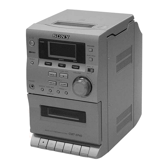
Photo: HCD-EP40
CD Section
TAPE Section
SPECIFICATIONS
Compact disc and digital
Q Q
audio system
3
6 7
1 3
Semiconductor laser
(λ=780 nm)
Emission duration:
continuous
20 Hz - 20 kHz (±0.5 dB)
4-track 2-channel stereo
50 - 13 000 Hz (±3 dB),
using Sony TYPE I
cassette
87.5 - 108.0 MHz
FM lead antenna
10.7 MHz
530 - 1 710 kHz
(with the interval set at
10 kHz)
531 - 1 602 kHz
(with the interval set at
9 kHz)
531 -1 602 kHz
(with the interval set at
9 kHz)
531 - 1 602 kHz
(with the interval set at
9 kHz)
530 - 1 710 kHz
(with the interval set at
10 kHz)
Built-in ferrite bar antenna
450 kHz
COMPACT DISC DECK RECEIVER
u163
.
2 9
9 4
2 8
Canadian Model
Australian Model
AEP Model
CD Mechanism Type
Tape Transport Mechanism Type
General
Power requirements
US, Canadian models:
120 V AC, 60 Hz
1 5
0 5
8
2 9
9 4
AEP, UK models:
230 V AC, 50/60 Hz
Australian model:
230 V AC, 50/60 Hz
Mexican model:
120 V AC, 60 Hz
Argentine model:
220 V AC, 50/60 Hz
Taiwan model:
110 V AC, 60 Hz
Other models:
230 V AC, 50/60 Hz
Power consumption
US model:
25 W
Canadian model:
25 W
AEP, UK models:
30 W
0.9 W (in the standby
mode)
Other models:
30 W
Approx. 145 × 238 × 238 mm
Dimensions (w/h/d):
Mass:
Approx. 2.8 kg
Design and specifications are subject to change
without notice.
m
co
9 9
US Model
E Model
HCD-EP30
UK Model
HCD-EP30/EP40
CS-21SC-1280
TCM125-2
2 8
9 9
Advertisement
Table of Contents

Related Manuals for Sony HCD-EP30


Summary of Contents for Sony HCD-EP30
- Page 1 Canadian Model Ver 1.0 2001.04 E Model Australian Model HCD-EP30 AEP Model UK Model HCD-EP30/EP40 HCD-EP30/EP40 are the amplifier, CD player, tape deck and tuner section in CMT-EP30/EP40. Photo: HCD-EP40 CD Section CD Mechanism Type CS-21SC-1280 TAPE Section Tape Transport Mechanism Type...
-
Page 2: Table Of Contents
HCD-EP30/EP40 3 7 63 1515 0 TABLE OF CONTENTS SERVICING NOTES ..........4 GENERAL ..............5 DISASSEMBLY 3-1. Disassembly Flow ............7 3-2. Front Panel Section ............8 3-3. MAIN Board ..............8 3-4. CD Cabinet Section ............9 3-5. - Page 3 OPERATION. REPLACE THESE COMPONENTS WITH DE FONCTIONNEMENT. NE REMPLACER CES COM- SONY PARTS WHOSE PART NUMBERS APPEAR AS POSANTS QUE PAR DES PIÈCES SONY DONT LES SHOWN IN THIS MANUAL OR IN SUPPLEMENTS PUB- NUMÉROS SONT DONNÉS DANS CE MANUEL OU LISHED BY SONY.
-
Page 4: Servicing Notes
HCD-EP30/EP40 SECTION 1 SERVICING NOTES 3 7 63 1515 0 • MODEL IDENTIFICATION NOTES ON HANDLING THE OPTICAL PICK-UP – Bottom View – BLOCK OR BASE UNIT The laser diode in the optical pick-up block may suffer electro- static break-down because of the potential difference generated by the charged electrostatic load, etc. -
Page 5: General
HCD-EP30/EP40 SECTION 2 This section is extracted from instruction manual. 3 7 63 1515 0 GENERAL LOCATION OF CONTROLS – Front Panel – 1 2 3 4 5 6 ql qk qj qh Cassette compartment qd (12) Remote sensor wk... -
Page 6: Remote Control
HCD-EP30/EP40 3 7 63 1515 0 Remote Control Setting the time Turn on the system. 1 2 3 4 Press CLOCK/TIMER/SLEEP SET on the remote. The clock indication appears. Press TUNING/CLOCK/TIMER + or — on the remote repeatedly to set the time. -
Page 7: Disassembly
HCD-EP30/EP40 SECTION 3 DISASSEMBLY 3 7 63 1515 0 • This set can be disassembled in the order shown below. 3-1. DISASSEMBLY FLOW 3-2. FRONT PANEL SECTION (Page 8) 3-6. TAPE MECHANISM DECK 3-3. MAIN BOARD 3-4. CD CABINET SECTION... -
Page 8: Front Panel Section
HCD-EP30/EP40 3 7 63 1515 0 Note: Follow the disassembly procedure in the numerical order given. 3-2. FRONT PANEL SECTION 2 antenna cover cabinet 3 two screws (BTP2.6 × 10) 6 claw 5 two screws (+K3 × 5) 1 screw (BVTP3 ×... -
Page 9: Cd Cabinet Section
HCD-EP30/EP40 3 7 63 1515 0 3-4. CD CABINET SECTION 2 CD cabinet section 1 two screws (BTP2.6 × 8) 3-5. CD MECHANISM DECK (CS-21SC-1280) L 13942296513 7 vibration proof rubber 6 two spring clamps (brown) 8 CD mechanism deck (CS-21SC-1280) -
Page 10: Tape Mechanism Deck (Tcm125-2)
HCD-EP30/EP40 3 7 63 1515 0 3-6. TAPE MECHANISM DECK (TCM125-2) 2 two screws (BTP2.6 × 6) 1 connector (CN701) 6 two screws (BVTP3 × 10) 7 tape mechanism deck (TCM125-2) 4 cassette board 6 two screws (BVTP3 × 10) 5 Open the cassette lid. -
Page 11: Mechanical Adjustments
HCD-EP30/EP40 SECTION 4 SECTION 5 MECHANICAL ADJUSTMENTS ELECTRICAL ADJUSTMENTS 3 7 63 1515 0 PRECAUTION PRECAUTION 1. Clean the following parts with a denatured-alcohol-moistened 1. Setting swab : MEGA BASS switch : OFF record/playback head pinch roller erase head... - Page 12 HCD-EP30/EP40 3 7 63 1515 0 Record/Playback Head Azimuth Adjustment Adjustment Location: Record/Playback/Erase Head. Procedure: 1. Mode: Playback (FWD) test tape P-4-A063 level meter (6.3 kHz, –10 dB) 32 Ω – HEADPHONE board PHONES jack (JK401) 2. Turn the adjustment screw and check output peaks. If the peaks do not match for L-CH and R-CH, turn the adjustment screw so that outputs match within 1dB of peak.
- Page 13 HCD-EP30/EP40 3 7 63 1515 0 no mark : US, Canadian, E, Australian models 0 dB=1 µV TUNER SECTION < > : AEP, UK models [AM] AM FREQUENCY COVERAGE ADJUSTMENT Setting: Adjustment Part Frequency Display Reading on Digital Voltmeter...
- Page 14 HCD-EP30/EP40 3 7 63 1515 0 Adjustment Location and Connecting Points – MAIN BOARD (Component Side) – L104 FM Frequency Coverage Adjustment TC102 AM Tracking L110 Adjustment T102 L103 FM Tracking Adjustment AM Frequency Coverage Adjustment TC101 L 13942296513 –...
-
Page 15: Diagrams
HCD-EP30/EP40 SECTION 6 3 7 6 3 1 5 1 5 0 DIAGRAMS 6-1. NOTE FOR PRINTED WIRING BOARDS AND SCHEMATIC DIAGRAMS • Circuit Boards Location Note on Printed Wiring Board: Note on Schematic Diagram: • All capacitors are in µF unless otherwise noted. pF: µµF •... -
Page 16: Schematic Diagram - Main Board (1/2)
HCD-EP30/EP40 3 7 6 3 1 5 1 5 0 6-2. SCHEMATIC DIAGRAM – MAIN Board (1/2) – • • See page 23 for Waveforms. See page 24 for IC Block Diagrams. L104 TP10 MAIN BOARD (1/2) FM FREQUENCY... -
Page 17: Schematic Diagram - Main (2/2)/Headphone Boards
HCD-EP30/EP40 3 7 6 3 1 5 1 5 0 6-3. SCHEMATIC DIAGRAM – MAIN (2/2)/HEADPHONE Boards – • See page 24 for IC Block Diagram. MAIN BOARD (Page 16) (1/2) (Page 21) (Page 21) MAIN BOARD (2/2) CN201... -
Page 18: Printed Wiring Boards - Main/Headphone Boards
HCD-EP30/EP40 3 7 6 3 1 5 1 5 0 6-4. PRINTED WIRING BOARDS – MAIN/HEADPHONE Boards – • See page 15 for Circuit Boards Location. • Semiconductor Location Ref. No. Location L110 AM FERRITE-ROD D101 ANTENNA D102 D103... -
Page 19: Printed Wiring Board - Cassette Board
HCD-EP30/EP40 3 7 6 3 1 5 1 5 0 6-5. PRINTED WIRING BOARD – CASSETTE Board – • 6-6. SCHEMATIC DIAGRAM – CASSETTE Board – See page 15 for Circuit Boards Location. • See page 23 for Waveforms. -
Page 20: Printed Wiring Board - Display Board
HCD-EP30/EP40 3 7 6 3 1 5 1 5 0 6-7. PRINTED WIRING BOARD – DISPLAY Board – • See page 15 for Circuit Boards Location. • Semiconductor Location Ref. No. Location DISPLAY BOARD IC603 D619 TIMER D621 D601... -
Page 21: Schematic Diagram - Display Board
HCD-EP30/EP40 3 7 6 3 1 5 1 5 0 6-8. SCHEMATIC DIAGRAM – DISPLAY Board – • See page 23 for Waveform. DISPLAY BOARD IC603 LIQUID CRYSTAL DISPLAY D619 RESET SIGNAL SW608 SEL2215S-CD TIMER SW611 GENERATOR SW601 SW612... -
Page 22: Schematic Diagram - Power Board
HCD-EP30/EP40 3 7 6 3 1 5 1 5 0 6-9. SCHEMATIC DIAGRAM – POWER Board – POWER BOARD Q404 +6V REGULATOR TR402 POWER C421 0.001 250V TRANSFORMER 8050D RL401 MTZJ-6.8B 2.2k 2.2k 8050D Q401–403 POWER ON/OFF C404 0.022... -
Page 23: Printed Wiring Board - Power Board
HCD-EP30/EP40 3 7 6 3 1 5 1 5 0 • Waveforms 6-10. PRINTED WIRING BOARD – POWER Board – • See page 15 for Circuit Boards Location. – DISPLAY Board – – MAIN Board – – CASSETTE Board –... - Page 24 HCD-EP30/EP40 3 7 6 3 1 5 1 5 0 • IC Block Diagrams IC203 LC75392 – MAIN Board – LVROUT RVROUT IC101 LA1823 LVRIN RVRIN GND2 VCC2 MUTE LTOUT RTOUT PHASE PILOT – DECODER COMP LTCOM RTCOM ST SW...
-
Page 25: Ic Pin Function Description
HCD-EP30/EP40 3 7 63 1515 0 6-11. IC PIN FUNCTION DESCRIPTION • DISPLAY BOARD IC601 µPD753016AGC-F31-3B9 (SYSTEM CONTROLLER, LIQUID CRYSTAL DISPLAY DRIVER) Pin No. Pin Name Description 1 to 20 S12 to S31 Segment drive signal output to the liquid crystal display (D621) -
Page 26: Exploded Views
HCD-EP30/EP40 SECTION 7 EXPLODED VIEWS 3 7 63 1515 0 NOTE: • Items marked “*” are not stocked since they • -XX and -X mean standardized parts, so they The components identified by mark 0 or dotted line with mark 0 are may have some difference from the original are seldom required for routine service. -
Page 27: Front Panel Section-1
HCD-EP30/EP40 3 7 63 1515 0 7-2. FRONT PANEL SECTION-1 L 13942296513 not supplied Ref. No. Part No. Description Remark Ref. No. Part No. Description Remark 4-235-953-01 VOL. SWING KNOB 4-235-942-01 CASS PWB MOUNTING BKT (A) 4-235-950-01 SWING SHAFT A-4726-711-A CASSETTE BOARD, COMPLETE 4-235-939-01 VOL. -
Page 28: Front Panel Section-2
HCD-EP30/EP40 3 7 63 1515 0 7-3. FRONT PANEL SECTION-2 not supplied L 13942296513 Ref. No. Part No. Description Remark Ref. No. Part No. Description Remark 4-235-995-01 RUBBER FOOT A-4726-712-A DISPLAY BOARD, COMPLETE (EP40) 4-235-975-01 FRONT PANEL (EP30) A-4726-785-A DISPLAY BOARD, COMPLETE (EP30: AEP, UK) -
Page 29: Cd Cabinet Section
HCD-EP30/EP40 3 7 63 1515 0 7-4. CD CABINET SECTION SW600 L 13942296513 Ref. No. Part No. Description Remark Ref. No. Part No. Description Remark 4-235-971-01 PLASTIC COVER 4-235-970-01 NSX1 PUSH ROD 4-236-280-01 RUBBER, VIBRATION PROOF (PINK) 4-235-990-01 CD EJECT SPRING... -
Page 30: Electrical Parts List
HCD-EP30/EP40 SECTION 8 3 7 63 1515 0 ELECTRICAL PARTS LIST CASSETTE NOTE: • Due to standardization, replacements in the • Items marked “*” are not stocked since they The components identified by mark 0 or dotted line with mark parts list may be different from the parts speci- are seldom required for routine service. - Page 31 HCD-EP30/EP40 3 7 63 1515 0 CASSETTE DISPLAY Ref. No. Part No. Description Remark Ref. No. Part No. Description Remark D610 8-719-991-33 DIODE 1SS133T-77 R733 1-249-429-11 CARBON 1/4W D611 8-719-991-33 DIODE 1SS133T-77 R734 1-249-437-11 CARBON 1/4W D612 8-719-991-33 DIODE 1SS133T-77...
- Page 32 HCD-EP30/EP40 3 7 63 1515 0 DISPLAY HEADPHONE MAIN Ref. No. Part No. Description Remark Ref. No. Part No. Description Remark R629 1-249-417-11 CARBON 1/4W A-4726-714-A HEADPHONE BOARD, COMPLETE R631 1-249-437-11 CARBON 1/4W *************************** R632 1-249-437-11 CARBON 1/4W < JACK >...
- Page 33 HCD-EP30/EP40 3 7 63 1515 0 MAIN Ref. No. Part No. Description Remark Ref. No. Part No. Description Remark C145 1-162-282-31 CERAMIC 100PF C249 1-130-475-00 FILM 0.0022uF 5% C146 1-162-294-31 CERAMIC 0.001uF C250 1-126-964-11 ELECT 10uF C251 1-130-491-00 FILM 0.047uF...
- Page 34 HCD-EP30/EP40 3 7 63 1515 0 MAIN Ref. No. Part No. Description Remark Ref. No. Part No. Description Remark D102 8-719-991-33 DIODE 1SS133T-77 Q311 8-729-194-57 TRANSISTOR 2SC945-P D103 8-719-070-77 DIODE SVC201SPA-M1-AC D104 8-719-070-77 DIODE SVC201SPA-M1-AC Q312 8-729-116-82 TRANSISTOR 2SD1616-L...
- Page 35 HCD-EP30/EP40 3 7 63 1515 0 MAIN POWER Ref. No. Part No. Description Remark Ref. No. Part No. Description Remark R211 1-249-424-11 CARBON 3.9K 1/4W R315 1-249-437-11 CARBON 1/4W R316 1-249-417-11 CARBON 1/4W R212 1-249-435-11 CARBON 1/4W R317 1-247-883-00 CARBON...
- Page 36 HCD-EP30/EP40 3 7 63 1515 0 POWER Ref. No. Part No. Description Remark Ref. No. Part No. Description Remark < CAPACITOR > < RELAY > C402 1-101-005-00 CERAMIC 22000PF 0 RL401 1-755-446-11 RELAY (AEP, UK, EA, SP, AR, AUS)
- Page 37 HCD-EP30/EP40 3 7 63 1515 0 MEMO L 13942296513 u163 http://www.xiaoyu163.com...
- Page 38 HCD-EP30/EP40 3 7 63 1515 0 REVISION HISTORY Clicking the version allows you to jump to the revised page. Also, clicking the version at the upper right on the revised page allows you to jump to the next revised page.
Need help?
Do you have a question about the HCD-EP30 and is the answer not in the manual?
Questions and answers