
Related Manuals for LG LAC-M5600


Summary of Contents for LG LAC-M5600
- Page 1 CAR CD/MP3/WMA RECEIVER SERVICE MANUAL CAUTION BEFORE SERVICING THE UNIT, READ THE “SAFETY PRECAUTIONS” IN THIS MANUAL. MODEL:LAC-M5600/LAC-UA560 P/N : AFN31552406 AUGUST, 2006...
- Page 2 [CONTENTS] ❍ SECTION 1.GENERAL • SERVICING PRECAUTIONS ..........1-2 •...
-
Page 3: Section 1. Summary
SECTION 1. SUMMARY ❏ SERVICING PRECAUTIONS ❶ Always disconnect the power source before: 1) Removing or reinstalling any component, circuit board, module or any other instrument assembly. 2) Disconnecting or reconnecting any instrument electrical plug or other electrical connection. 3) Connecting a test substitute in parallel with an electrolytic capacitor in the instrument. CAUTION: A wrong part substitution or incorrect polarity installation of electrolytic capacitors may result in an explosion hazard. -
Page 4: Esd Precautions
❏ ESD PRECAUTIONS Electrostatically Sensitive Devices (ESD) Some semiconductor (solid state) devices can be damaged easily by static electricity. Such components commonly are called Electrostatically Sensitive Devices (ESD). Examples of typical ESD devices are integrated circuits and some field-effect transistors and semiconductor chip components. The following techniques should be used to help reduce the incidence of component damage caused by static electricity. -
Page 5: Specifications
❏ SPECIFICATIONS MP3/WMA Disc compatibility with this unit is limited as follows: 1. Sampling Frequency / 8 - 48kHz (MP3) 22.05 - 48kHz (WMA) 2. Bit rate / within 8 - 320kbps (include VBR) (MP3) 32 -320kbps (WMA) 3. CD-R/CD-RW physical format should be “ISO 9660” 4. -
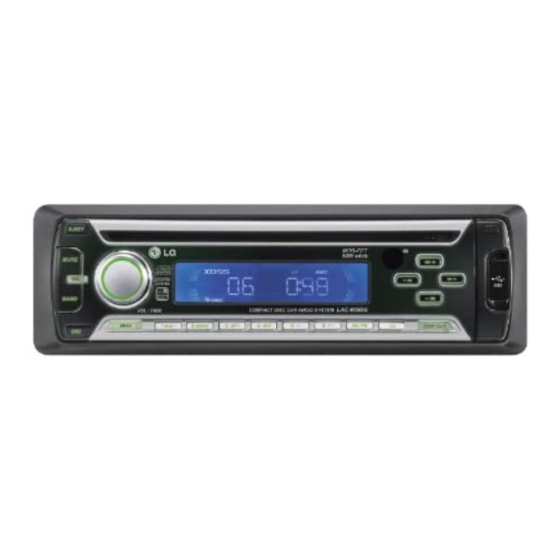
Page 6: Location Of Customer Controls
❏ LOCATION OF CUSTOMER CONTROLS 1. Front Panel (LAC-M5600) EJECT MUTE BAND AS/PS XDSS SC AN DISP/CLK [EJECT] 12 • PRESET STATION [1-6] POWER / VOLUME [PWR/VOL] • MP3 TRACK +10/-10 DISPLAY WINDOW • FOLDER UP/DOWN [F+/F-] DISC SLOT • SHUFFLE [SHF] REMOTE SENSOR •... -
Page 7: Remote Control
3. Remote control POWER [PWR] / MUTE SELECTION [SEL] SOURCE [SRC] PLAY / PAUSE INTRO SCAN [SCAN] SHUFFLE [SHF] • MP3 TRACK +10 • FOLDER UP [F+] • CD SKIP / SEARCH • SEEK / TUNE [BAND] 10 VOLUME UP / DOWN 11 NUMBER [#] 12 REPEAT [RPT]... -
Page 8: Basic Installation
❏ INSTALLATION • Basic Installation Before installing, make sure that the ignition switch is set to Bend the claws OFF and remove the terminal of the car battery to avoid according to the thickness short-circuiting. of the dashboard 1 Remove the existing receiver unit. 2 Make the necessary connections. -
Page 9: Connection Diagram
❏ CONNECTION DIAGRAM Before connecting, make sure that the ignition switch is set to OFF, and remove the battery terminal to avoid short circuits. From antenna To the wiring of the vehicle colors of leads. PHONE MUTE (ORANGE) GROUND(-) (BLACK) DIMMER (PINK) DIMMER SWITCH TO IGNITION (RED) -
Page 10: Speaker Connections
Speaker Connections • BLACK : This lead is for the ground connection. • ORANGE : This lead is for the phone line connection. • PINK : This lead is for the dimmer line connection. • RED : This lead is for connection to the power supply terminal when the ignition switch is set to ACC. - Page 11 - 1-10 -...
-
Page 12: Section 2. Electrical
SECTION 2. ELECTRICAL ❏ ELECTRICAL TROUBLESHOOTING GUIDE 1. No Power. Any Key power on. Check power supply circuitry. Is power turnd on? IC802 Pin Check loading supply circuitry. DISC loading? IC802 Pin Check laser circuitry. Does initial reading occur? Q501, IC506 Check focusing circuitry. - Page 13 2. LCD light abnornal. Any Key power on. (without DISC) Power supply circuitry defective. Check voltage in the power • Check Q403, Q404, Q406, Do display LCD then light? supply circuitry. Q407, IC802 Pin Is u-com IC401 pin reset • Reset circuit defective. circuit normal? IC901 Surrounding circuit defective.
- Page 14 3. Initial reading is not carried out. Defective Check the Voltage change of Slide motor moves. Connector. (PN502) PN502 Pin (6.4~6.8V). (With disc) Check the Voltage change of PN506 Defective IC506 76 77 Pins . (1.4V~1.8V). Spindle motor turns. Check the Data transmission (Refer to FIG3.) 70 72 from IC510 pins...
-
Page 15: Open Close
When laser does not light. Is “2.4V~3.4V” applied to pin42 of IC506? ➀ 3.4V ➁ 2.4V) Did pickup return to Is data transferred Defective MICOM (IC510) innermost circular? from IC510? Does voltage appear at Defective IC504 IC504 Pins 13 14 Defective slide motor and/or connector(PN504) Is defect output from LMT... - Page 16 When laser light. Laser lights? Check the signal FOCUS Defective IC506 SEARCH of IC506 Pin (Refer to FIG1.) Check the signal of IC504 Pins 15 16 Defective IC506 (Refer to FIG1.) • Degraded laser diode • Defective PICK-UP When SPINDLE motor dose not turn Check the change for SPDO Voltage Defective IC506...
-
Page 17: Waveforms Of Major Check Point
❏ WAVEFORMS OF MAJOR CHECK POINT FIG1) FOCUS CONTOR SIGNAL FIG2) TRACKING CONTOR SIGNAL PN504:F-[PIN1] PN504:T+[PIN2] IC506:FOP IC506:TRP [PIN25] [PIN24] R517:FE R517:TE PN506:F+[PIN4] PN506:F+[PIN3] FIG3) SPINDLE CONTOR SIGNAL FIG4) PD,RFOUT PN504: IC506: SP+[PIN7] PD [41] PD/MD IC506: IC506: PLLF [PIN54] RFOUT [46] IC506: PLLF... -
Page 18: Internal Block Diagram Of Ics
❏ INTERNAL BLOCK DIAGRAM of ICs UPD78F0546 1) Block Diagram - 2-7 -... - Page 19 2) Micom port Assignment 80 79 78 77 76 75 7473 72 71 70 69 68 67 66 65 6463 62 61 P120/INTPO/EXLVI AVSS AVREF P10/SCK10/TXD0 P11/SI10/RXD0 P12/SO10 80pin QFP RESET P13/TXD6 P124/XT2/EXCLKS P14/RXD6 P123/XT1 P15/TOH0 IC/FLMD0 P16/TOH1/INTP5 P122/X2/EXCLK P17/TI50/TO50 P121/X1 P30/INTP1 REGC...
-
Page 20: Pin Descriptions
2) Pin Descriptions - 2-9 -... - Page 21 - 2-10 -...
- Page 22 BD3805F (SCF built-in sound processor) 1) BLOCK DIAGRAM - 2-11 -...
- Page 23 HA13173 (Multi Voltage Regulator IC) - 2-12 -...
- Page 24 TA8275H (Bipolar Liner) 1) Block Diagram - 2-13 -...
- Page 25 AM5810 (Motor Driver IC) 1) Block Diagram - 2-14 -...
-
Page 26: Pin Function
3) Pin Function - 2-15 -... -
Page 27: Pin Layout
MN6627954 (DSP IC) 1) Pin Lay Out 75 74 73 72 71 70 69 68 67 66 65 64 63 62 61 60 59 58 57 56 55 54 53 52 51 DVDD2 ARFFB IOVDD1 ARFOUT DVSS2 ARFDC NTEST2 AVDO2 RF IN RFOUT MTEST... - Page 28 2) Block Diagram NTEST2 NTEST TIMING MICRO COMPUTER DSL / PLL / VCO NSRVMONON * TXTCK GENERATOR INTERFACE [DSLPLL] NRST [GEN] [MCIF] * TXTD * DQSY SPINDLE SUBCODE EFM DEMODULATION AVDD2 (SBCK) SERVO INTERFACE AVSS2 SYNC INTERPOLATION [SPD] (SUBC) [DEMECC] A,B,C,D,E,F CIRC ECC CDROM ECC...
- Page 29 3) Pin Function Pin no. Symbol Function Adress signal output for DRAM11 Adress signal output for DRAM9 Adress signal output for DRAM8 Adress signal output for DRAM7 Adress signal output for DRAM6 Adress signal output for DRAM5 Adress signal output for DRAM4 Writing enable signal output for DRAM NCAS CAS control signal output for DRAM...
- Page 30 KIA78R05 (Terminal Low Drop Voltage Regulator) 1) Block Diagram BAOOCCOWFP (IA Low Dropout Voltage Regulator) 1) Block Diagram N.C. Vref Driver VOUT - 2-19 -...
-
Page 31: General Description
OTI6888 (USB Host Controller) 1) GENERAL DESCRIPTION OTi-6889 is the USB mini host controller with popular compressed media format bit-stream interface, such as MP3, WMA. The controller embedded the USB 1.1 host/device function; the function provides the ability that can be connected to the USB device and PC via USB port. The user may store the MP3/WMA songs in the USB mass storage device and play them through the OTi-6889 bit-stream interface. -
Page 32: Block Diagram (Whole)
❏ BLOCK DIAGRAM (WHOLE) 2-21 2-22... -
Page 33: Block Diagram (Cdp)
❏ BLOCK DIAGRAM (CDP) 2-23 2-24... -
Page 34: Main Schematic Diagram
❏ SCHEMATIC DIAGRAMS • MAIN SCHEMATIC DIAGRAM 2-25 2-26... -
Page 35: Front Schematic Diagram
• FRONT SCHEMATIC DIAGRAM 2-27 2-28... -
Page 36: Usb Schematic Diagram
• USB SCHEMATIC DIAGRAM 2-29 2-30... - Page 37 • USB(SUB) SCHEMATIC DIAGRAM 2-31 2-32...
- Page 38 • CD SCHEMATIC DIAGRAM 2-33 2-34...
-
Page 39: Printed Circuit Board Diagrams
❏ PRINTED CIRCUIT BOARD DIAGRAMS • MAIN P.C. BOARD DIAGRAM (BOTTOM) 2-35 2-36... - Page 40 • FRONT/USB JACK P.C. BOARD DIAGRAM (TOP) • LED P.C. BOARD (BOTTOM) • LED P.C. BOARD (TOP) • FRONT/USB JACK P.C. BOARD DIAGRAM (BOTTOM) 2-37 2-38...
- Page 41 • CD P.C. BOARD (BOTTOM) • CD P.C. BOARD (TOP) 2-39 2-40...
-
Page 42: Section 3. Exploded Views
SECTION 3. EXPLODED VIEWS ❏ CABINET AND MAIN FRAME SECTION Service purchase Guidance A40 compose by Front PWB ASSY, Lighting PWB ASSY (A40L) & USB Jack ASSY (A40U). Because 3 kinds of PWB Assembly is worked in PWB negative plate of one, supply is smooth if require by A40 P/N in the case of Purchase Order. -
Page 43: Mechanism (Pick-Up)
❏ MECHANISM (PICK-UP)
Need help?
Do you have a question about the LAC-M5600 and is the answer not in the manual?
Questions and answers