Table of Contents
Advertisement
Quick Links
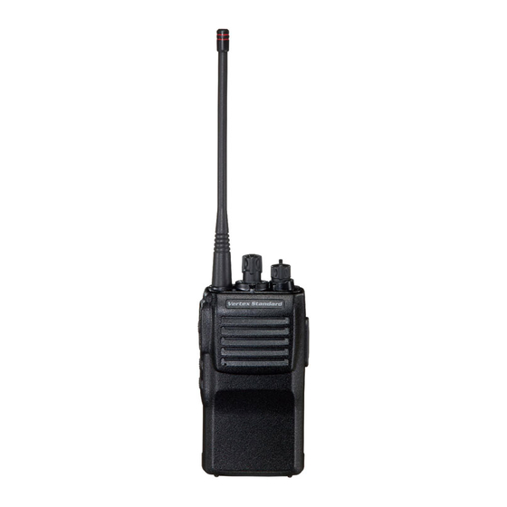
VHF FM Transceiver
VX-410/-420 series
Service Manual
©2004 VERTEX STANDARD CO., LTD.
This manual provides technical information necessary for servicing the VX-410/-420 series FM Transceiver.
Servicing this equipment requires expertise in handling surface-mount chip components. Attempts by non-qualified
persons to service this equipment may result in permanent damage not covered by the warranty, and may be illegal in
some countries.
Two PCB layout diagrams are provided for each double-sided circuit board in the transceiver. Each side of is referred
to by the type of the majority of components installed on that side ("leaded" or "chip-only"). In most cases one side has
only chip components, and the other has either a mixture of both chip and leaded components (trimmers, coils, electrolytic
capacitors, ICs, etc.), or leaded components only.
While we believe the technical information in this manual to be correct, VERTEX STANDARD assumes no liability
for damage that may occur as a result of typographical or other errors that may be present. Your cooperation in pointing
out any inconsistencies in the technical information would be appreciated.
Operating Manual Reprint ................................... 2
Cloning ..................................................................... 7
Specifications .......................................................... 8
Exploded View & Miscellaneous Parts .............. 9
Block Diagram .......................................................11
Circuit Description ............................................... 13
Alignment .............................................................. 15
EC050N90A
VX-410 series
Contents
VERTEX STANDARD CO., LTD.
4-8-8 Nakameguro, Meguro-Ku, Tokyo 153-8644, Japan
VERTEX STANDARD
US Headquarters
10900 Walker Street, Cypress, CA 90630, U.S.A.
YAESU EUROPE B.V.
P.O. Box 75525, 1118 ZN Schiphol, The Netherlands
YAESU UK LTD.
Unit 12, Sun Valley Business Park, Winnall Close
Winchester, Hampshire, SO23 0LB, U.K.
VERTEX STANDARD HK LTD.
Unit 5, 20/F., Seaview Centre, 139-141 Hoi Bun Road,
Kwun Tong, Kowloon, Hong Kong
VX-420 series
Board Unit (Schematics, Layouts & Parts)
MAIN Unit ............................................................... 19
DUMMY Unit .......................................................... 34
Optional Units (Schematics, Layouts & Parts)
FVP-25 Encryption / DTMF Pager Unit .............. 35
VTP-50 VX-Trunk Unit .......................................... 37
DVS-5 Voice Storage Unit ..................................... 39
Advertisement
Table of Contents

Related Manuals for Vertex VX-410 series


Summary of Contents for Vertex VX-410 series
-
Page 1: Table Of Contents
ICs, etc.), or leaded components only. While we believe the technical information in this manual to be correct, VERTEX STANDARD assumes no liability for damage that may occur as a result of typographical or other errors that may be present. Your cooperation in pointing out any inconsistencies in the technical information would be appreciated. -
Page 2: Operating Manual Reprint
LED Indicator Battery Pack Installation and Removal Glows Green Monitor on (or Side 1, 2 switch is activated : VX-410 series only) Ì To install the battery, hold the transceiver with your Blinking Green Busy Channel (or SQL off) Glows Red... - Page 3 Operating Manual Reprint Operation Ì Press and hold in the Soft key Preliminary Steps Ì Install a charged battery pack onto the transceiver, as assigned to “MONITOR” for described previously. more than 1 seconds (or press Ì Screw the supplied antenna onto the Antenna jack. the MONITOR key twice) to Never attempt to operate this transceiver without an quiet the noise and resume nor-...
-
Page 4: Description Of Operating Functions
(quiet) Noise and Tone squelch action. below, and their functions are explained in the next chap- Low Power ter. For further details, contact your VERTEX STAN- DARD dealer. Press (or Press and hold) the assigned Soft key to For future reference, check the box next to each func- set the radio’s transmitter to the “Low Power”... - Page 5 Operating Manual Reprint Description of Operating Functions Follow-Me Scan Add/Del “Follow-Me” Scan feature checks a User-assigned The Add/Del feature allows the user to arrange a Priority Channel regularly as you scan the other custom Scan. channels. Thus, if only Channels 1, 3, and 5 (of the 8 Press (or Press and hold) the assigned Soft key to available channels) are designated for “Scanning,”...
- Page 6 This system allows paging and selective calling, tions are various uses. using DTMF tone sequences. For further details, contact your VERTEX STAN- When your radio is paged by a station bearing a DARD dealer tone sequence which matches yours, your radio’s squelch will open and the alert will sound.
-
Page 7: Cloning
“CLONE” (for VX-420 series; for VX-410 series, of the VX-410 series, no change will be observed at the TX/BUSY indicator on the top of the radio will this point. -
Page 8: Specifications
Specifications GENERAL Specifications Frequency Range: 146 - 174 MHz Number of Channels: 32 channels Channel Spacing: 2.5 / 6.25 kHz PLL Steps 5 / 6.25 kHz Power Supply voltage: 7.5 VDC ± 10% Operating Temperature Range: –22°F to +140°F (–30°C to +60°C) Frequency Stability: ±2.5 ppm Dimensions (WHD):... -
Page 9: Exploded View & Miscellaneous Parts
Exploded View & Miscellaneous Parts RA0585700 WINDOW ASSY (VX-420N) RA0545100 (Lot. 1~) (W/ DOUBLE FACE APE) RA054510B (Lot. 2~) FRONT CASE ASSY (W/ LIGHT GUIDE,NAME PLATE,SP NET,SPEAKER,PACKING PAD, RA0173500 Ž PTT KNOB,SHEET(MIC),CR SPONGE RUBBER,WINDOW ASSY) Ž R6147510 RA054570A (Lot. 1~) RING NUT (x 2 pcs) RA054570B (Lot. - Page 10 Note:...
-
Page 11: Block Diagram
Block Diagram... - Page 12 Note:...
-
Page 13: Circuit Description
Circuit Description Receive Signal Path pin 19 of the microprocessor Q1047 (LC87F74C8A). If Incoming RF from the antenna jack is delivered to the no carrier is received, this signal causes pin 19 of Q1047 RF Unit and passes through a low-pass filter consisting of to go high and pin 30 to go high. -
Page 14: Transmit Inhibit
Circuit Description Q1014 (2SK2596BXTL), and then the amplified trans- section of Q1051, before being sent to the programmable mit signal is applied to the final amplifier Q1008 divider section of Q1051. (RD07MVS1), which delivers up to 5 watts of output The data latch section of Q1051 also receives serial power. -
Page 15: Alignment
68°~ 86°F (20° and 30°C). When the transceiver is brought by the warranty policy. Also, Vertex Standard must re- into the shop from hot or cold air, it should be allowed serve the right to change circuits and alignment proce- time to come to room temperature before alignment. - Page 16 Alignment The alignment tool outline Set up the test equipment as shown below for trans- ceiver alignment, and apply 7.5V DC power to the trans- Installation of the Alignment tool ceiver. The “alignment mode” is a software-based protocol, accessed by an “Alignment Mode” command from the computer while switching the transceiver on.
-
Page 17: Reference Frequency
Alignment PLL VCV (Varactor Control Voltage) Transmitter Output Power Ì Connect the DC voltmeter between TP1045 on the Ì Set the transceiver to CH 2 (band center). Ì To adjustment, click the left mouse button on the “RF Main Unit and ground. Ì... - Page 18 Alignment CTCSS Deviation DTMF Deviation Ì Set the transceiver to CH 2 (band center). Ì Set the transceiver to CH 2 (band center). Ì To adjustment, click the left mouse button on the Ì To adjustment, click the left mouse button on the “CTCSS Modulation”...
-
Page 19: Main Unit
MAIN Unit Circuit Diagram Wide:0V Narrow:0V Wide:3.39V 4.78V 1.70V 4.42V Narrow:0V 0.75V 0.73V 0.51V 4.84V Wide:0V Narrow:0V 4.97V (0V) 2.45V (0.0V) 0.16V 0.78V (0.79V) 3.35V (4.11V) (2.50V) 0.30V 0V (0V) 0.16V <1.07V> 0.16V (4.95V) {0.44V} (4.67V) 1.69V 0.16V (1.74V) (0.83V) 0.48V (2.88V) Wide:0.36V... - Page 20 Note:...
- Page 21 MAIN Unit Parts Layout Side A NJM2070M CPH6102 (AB) DTA144EE (16) 2SC4154E (LE) BD4835FVE (DR) 12-22SURSYGC/S530-A2/TR8 (Q1005) (Q1007) (Q1039) (Q1006, 1034,1037, (Q1040) (D1039) 1044, 1045) LC87F74C8A (Q1047) NJM12904R (Q1054) IMZ2 (Z2) UMX1N (X1) 2SA1602A (MF) DTC114TE (04) DA221 (K) BR93L56RFVM-WTR (Q1003) (Q1002, 1063) (Q1004)
- Page 22 MAIN Unit Parts Layout Side B AK2342B M62364FP TA31136FN RD07MVS1 CPH6102 (AB) UMX1N (X1) 2SK3541 DTB123EK (F12) UMC5N (C5) DTC144EE (26) 2SC4154E (LE) DAN222 (N) (Q1021) (Q1015) (Q1048) (Q1008) (Q1012, 1017, 1058) (Q1013, 1018, 1059) (Q1011, 1038, (Q1022) (Q1043) (Q1028, 1031, 1032, (Q1016, 1027) (D1044, 1045) 1055)
- Page 23 MAIN Unit Parts List REF. DESCRIPTION VALUE TOL. MFR’S DESIG VXSTD P/N VERS. LOT. SIDE LAY ADR PCB with Components CB2541001 LCD ON CB2541002 LCD OFF Printed Circuit Board FR010400D C 1002 CHIP CAP. 0.001uF GRM36B102K50PT K22178809 C 1006 CHIP CAP. 0.001uF GRM36B102K50PT K22178809...
- Page 24 MAIN Unit REF. DESCRIPTION VALUE TOL. MFR’S DESIG VXSTD P/N VERS. LOT. SIDE LAY ADR C 1089 CHIP CAP. 33pF GRM36CH330J50PT K22178224 C 1090 CHIP CAP. 33pF GRM36CH330J50PT K22178224 C 1091 CHIP CAP. 0.1uF GRM36B104K10PT K22108802 C 1092 CHIP CAP. 0.01uF GRM36B103K16PT K22128804...
- Page 25 MAIN Unit REF. DESCRIPTION VALUE TOL. MFR’S DESIG VXSTD P/N VERS. LOT. SIDE LAY ADR C 1168 CHIP CAP. 0.1uF GRM36B104K10PT K22108802 C 1169 CHIP CAP. 0.1uF GRM36B104K10PT K22108802 C 1170 CHIP CAP. 0.1uF GRM36B104K10PT K22108802 C 1171 CHIP CAP. 470pF GRM36B471K50PT K22178805...
- Page 26 MAIN Unit REF. DESCRIPTION VALUE TOL. MFR’S DESIG VXSTD P/N VERS. LOT. SIDE LAY ADR C 1252 CHIP CAP. 0.1uF GRM36B104K10PT K22108802 C 1254 CHIP CAP. 390pF GRM36B391K50PT K22178804 C 1256 CHIP CAP. 100pF GRM36CH101J50PT K22178236 C 1257 CHIP CAP. 27pF GRM36CH270J50PT K22178222...
- Page 27 MAIN Unit REF. DESCRIPTION VALUE TOL. MFR’S DESIG VXSTD P/N VERS. LOT. SIDE LAY ADR D 1040 LED TLOU1008A(TAPE) G2070958 W/LCD D 1042 DIODE 1SS400G T2R G2070934 D 1043 DIODE 1SS400G T2R G2070934 D 1044 DIODE DAN222 TL G2070174 D 1045 DIODE DAN222 TL G2070174 D 1046 DIODE...
- Page 28 R 1021 CHIP RES. 1/16W 5% RMC1/16S 331JTH J24189019 R 1022 CHIP RES. 1/16W 5% RMC1/16S JPTH J24189070 R 1023 CHIP RES. 1/16W 5% RMC1/16S 473JTH J24189045 R 1024 CHIP RES. 1/16W 5% RMC1/16S 563JTH J24189046 Please contact VERTEX STANDARD.
- Page 29 MAIN Unit REF. DESCRIPTION VALUE TOL. MFR’S DESIG VXSTD P/N VERS. LOT. SIDE LAY ADR R 1024 CHIP RES. 8.2k 1/16W 5% RMC1/16S 822JTH J24189036 R 1025 CHIP RES. 1/16W 5% RMC1/16S JPTH J24189070 R 1026 CHIP RES. 4.7k 1/16W 5% RMC1/16S 472JTH J24189033 R 1027 CHIP RES.
- Page 30 MAIN Unit REF. DESCRIPTION VALUE TOL. MFR’S DESIG VXSTD P/N VERS. LOT. SIDE LAY ADR R 1091 CHIP RES. 2.2k 1/16W 5% RMC1/16S 222JTH J24189029 R 1092 CHIP RES. 1/16W 5% RMC1/16S 333JTH J24189043 R 1093 CHIP RES. 1/16W 5% RMC1/16S JPTH J24189070 R 1094 CHIP RES.
- Page 31 MAIN Unit REF. DESCRIPTION VALUE TOL. MFR’S DESIG VXSTD P/N VERS. LOT. SIDE LAY ADR R 1163 CHIP RES. 1/16W 5% RMC1/16S 220JTH J24189005 R 1164 CHIP RES. 1/16W 5% RMC1/16S 103JTH J24189037 R 1165 CHIP RES. 1/16W 5% RMC1/16S 102JTH J24189025 W/LCD R 1166 CHIP RES.
- Page 32 MAIN Unit REF. DESCRIPTION VALUE TOL. MFR’S DESIG VXSTD P/N VERS. LOT. SIDE LAY ADR R 1235 CHIP RES. 1/16W 5% RMC1/16S 101JTH J24189013 R 1236 CHIP RES. 1/16W 5% RMC1/16S JPTH J24189070 R 1237 CHIP RES. 1/16W 5% RMC1/16S 473JTH J24189045 R 1238 CHIP RES.
- Page 33 MAIN Unit REF. DESCRIPTION VALUE TOL. MFR’S DESIG VXSTD P/N VERS. LOT. SIDE LAY ADR S 1004 TACT SWITCH SKRTLAE010 N5090130 S 1005 TACT SWITCH SKRTLAE010 N5090130 TH1001 THERMISTOR TBPS1R103K440H5Q G9090067 TH1002 THERMISTOR ERTJ0EV473J G9090120 VR1001 POT. TP76N00N 20KA/SW RY-7513 J60800269 X 1001 XTAL SX-1319 7.3728MHz...
-
Page 34: Dummy Unit
DUMMY Unit Circuit Diagram Parts Layout Parts List REF. DESCRIPTION VALUE TOL. MFR’S DESIG VXSTD P/N VERS. LOT. SIDE LAY ADR PCB with Components CB2731001 Printed Circuit Board FR002510C C 4001 CHIP CAP. 0.0018uF GRM39B182M50PT K22174812 C 4002 CHIP CAP. 0.1uF GRM39B104K16PT K22124805... -
Page 35: Fvp-25 Encryption / Dtmf Pager Unit
FVP-25 Encryption / DTMF Pager Unit Circuit Diagram Parts Layout Side A Side B M64026FP LC73881 DTC144EU (26) (Q1001) (Q1002) (Q1003) - Page 36 FVP-25 Encryption / DTMF Pager Unit Parts List REF. DESCRIPTION VALUE TOL. MFR’S DESIG VXSTD P/N VERS. LOT. SIDE LAY ADR *** FVP-25 *** Printed Circuit Board FR005010F C 1001 CHIP CAP. 0.1uF GRM39B104K16PT K22124805 C 1002 CHIP CAP. 0.01uF GRM39B103M25PT K22144802 C 1003 CHIP CAP.
-
Page 37: Vtp-50 Vx-Trunk Unit
VTP-50 VX-Trunk Unit Circuit Diagram Parts Layout Side B Side A BR93LC56FV NJM2904V MC68HSC705C8A502 TA75S01F (SA) (Q1001) (Q1003) (Q1004) (Q1002) - Page 38 VTP-50 VX-Trunk Unit Parts List REF. DESCRIPTION VALUE TOL. MFR’S DESIG VXSTD P/N VERS. LOT. SIDE LAY ADR *** VTP-50 *** Printed Circuit Board FR002540C C 1002 CHIP CAP. 0.001uF GRM39B102K50PT K22174821 C 1003 CHIP CAP. 0.01uF GRM39B103M25PT K22144802 C 1003 CHIP CAP. 0.01uF GRM39B103K25PT K22144803...
-
Page 39: Dvs-5 Voice Storage Unit
DVS-5 Voice Storage Unit Circuit Diagram Parts Layout Side A Side B... - Page 40 DVS-5 Voice Storage Unit Parts List REF. DESCRIPTION VALUE TOL. MFR’S DESIG VXSTD P/N VERS. LOT. SIDE LAY ADR *** DVS-5 *** Printed Circuit Board FR010690D C 1001 CHIP CAP. 0.001uF GRM36B102K50PT K22178809 C 1002 CHIP CAP. 0.001uF GRM36B102K50PT K22178809 C 1003 CHIP TA.CAP.
- Page 41 Copyright 2004 VERTEX STANDARD CO., LTD. All rights reserved No portion of this manual may be reproduced without the permission of VERTEX STANDARD CO., LTD.
Need help?
Do you have a question about the VX-410 series and is the answer not in the manual?
Questions and answers