Table of Contents
Advertisement
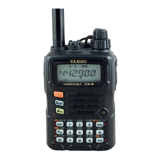
Dual-Band
Heavy Duty Submersible Transceiver
VX-6R
Technical Supplement
©2005 VERTEX STANDARD CO., LTD.
Specification ............................................................................................................................................ 2
Exploded View & Miscellaneous Parts ............................................................................................. 4
Block Diagram ........................................................................................................................................ 5
Interconnection Diagram ...................................................................................................................... 6
Circuit Description................................................................................................................................ 7
Alignment .............................................................................................................................................. 11
Board Unit (Schematics, Layouts & Parts)
CNTL Unit ....................................................................................................................................................................... 17
AF Unit ............................................................................................................................................................................ 27
RF Unit ............................................................................................................................................................................. 37
VCO Unit ......................................................................................................................................................................... 53
EH021M90A
Introduction
This manual provides the technical information necessary for servicing
the VX-6R Dual-Band Heavy Duty Submersible Transceiver.
Servicing this equipment requires expertise in handing surface-mount
chip components. Attempts by non-qualified persons to service this
equipment may result in permanent damage not covered by the war-
ranty, and may be illegal in some countries.
Two PCB layout diagrams provided for each double-sided board in
this transceiver. Each side of the board is referred to by the type of the
majority of components installed on that side ("Side A" or "Side B"). In
most cases one side has only chip components, and the other has either
a mixture of both chip and leaded components (trimmers, coils, electro-
lytic capacitors, ICs, etc.), or leaded components only.
While we believe the information in this manual to be correct,
VERTEX STANDARD assumes no liability for damage that may occur
as a result of typographical or other errors that may be present. Your
cooperation in pointing out any inconsistencies in the technical infor-
mation would be appreciated.
Contents
VERTEX STANDARD CO., LTD.
4-8-8 Nakameguro, Meguro-Ku, Tokyo 153-8644, Japan
VERTEX STANDARD
US Headquarters
10900 Walker Street, Cypress, CA 90630, U.S.A.
YAESU EUROPE B.V.
P.O. Box 75525, 1118 ZN Schiphol, The Netherlands
YAESU UK LTD.
Unit 12, Sun Valley Business Park, Winnall Close
Winchester, Hampshire, SO23 0LB, U.K.
VERTEX STANDARD HK LTD.
Unit 5, 20/F., Seaview Centre, 139-141 Hoi Bun Road,
Kwun Tong, Kowloon, Hong Kong
1
Advertisement
Table of Contents

Related Manuals for Vertex VX-6R


Summary of Contents for Vertex VX-6R
-
Page 1: Table Of Contents
ICs, etc.), or leaded components only. While we believe the information in this manual to be correct, VERTEX STANDARD assumes no liability for damage that may occur as a result of typographical or other errors that may be present. Your cooperation in pointing out any inconsistencies in the technical infor- mation would be appreciated. -
Page 2: Specification
Specifications General Rx 0.5 - 1.8 MHz (BC Band) Frequency Ranges: 1.8 - 30 MHz (SW Band) 30-76 (59) MHz (50 MHz HAM: USA version) 76 (59)-108 MHz (FM: USA version) 108-137 MHz (Air Band) 137-174 MHz (144 MHz HAM Band) 174-222 MHz (VHF-TV Band) 222-420 MHz (ACT1: Action Band 1: USA version) 420-470 MHz (430 MHz HAM Band) -
Page 3: Specifications
Specifications Transmitter High Low 3 Low 2 Low 1 RF Power Output: 144 MHz/430 MHz 5.0 W 2.5 W 1.0 W 0.3 W 220 MHz 1.5 W 1.0 W 0.5 W 0.2 W Variable Reactance F2D, F3E Modulation Type: ±5.0 kHz (F2D, F3E) Maximum Deviation: At least 60 dB below (@ High power) Spurious Emission:... -
Page 4: Exploded View & Miscellaneous Parts
Exploded View & Miscellaneous Parts VXSTD P/N Description Qty. U44104002 TAPTITE SCREW M2X4NI RA0653700 RA0645400 U9900180 TAPTITE SCREW 2X5SUS(O-RING) WINDOW DOUBLE FACE TAPE U9900179 TAPTITE SCREW 2X22SUS(O-RING) CP8159002 (DST:USA) U9900181 TAPTITE SCREW 2X3.5(CAP) CP8159003 (DST:EXP) CP8159004 (DST:EU) Non-designated parts are available only as part of a CP8159005 (DST:AUS) designated assembly. -
Page 5: Block Diagram
Block Diagram... -
Page 6: Interconnection Diagram
Interconnection Diagram... -
Page 7: Circuit Description
Circuit Description The VX-6R consists of a RF-UNIT, a CNTL-UNIT and (3) 60-300MHz Reception an AF-UNIT. The RF-UNIT contains the receiver front end, Received signals between 60 and 300 MHz pass PLL IC, power and switching circuits, and the VCO-UNIT through the Triplexer circuit, low-pass filter/high-pass for transmit and receive local signal oscillation. - Page 8 Circuit Description plication to RF amplifier Q1003 (2SC5277-D2-TL) and (7) Squelch Control Q1005 (2SC5277-D2-TL). The amplified RF signal is pass Signal components in the neighborhood of 15 kHz con- through the band-pass filter to first mixer Q1010 tained in the discriminator output pass through an active (2SC5277-D2-TL).
- Page 9 Circuit Description During CTCSS operation, the voice signal is mixed passes through TX diode switch D1046. RF output is with the TONE ENC subaudible tone signal from pin 43 passed by T/R switch and low-pass filter to suppress har- of the CPU and delivered to the RF-UNIT through jacks monics and spurious products before output to the an- J3003 and J1002.
- Page 10 Circuit Description Note:...
-
Page 11: Alignment
Alignment Introduction Required Test Equipment The VX-6R is carefully aligned at the factory for the RF Signal Generator with calibrated output level at 500 MHz specified performance across the amateur band. Realign- Deviation Meter (linear detector) ment should therefore not be necessary except in the event In-line Wattmeter with 5% accuracy at 500 MHz of a component failure. - Page 12 Alignment Internal System Alignment Routine Squelch Preset Tight (TLG) [136] Press the [ V/M ] button, then adjust the generator level This uses a programmed routine in the transceiver to –4.0 dBµ, then press the [ V/M ] button. Rotate the DIAL which simplifies many previously complex discrete com- ponent settings and adjustments with digitally-controlled to select the next setting.
- Page 13 Alignment Wide-FM S-Meter Full-Scale Adjustment (S9) [83] TX Deviation Adjustment (DEU) [65] Press the [ V/M ] button, then adjust the generator level Inject a 1 kHz audio tone at a level of 50mV (rms) to the to +25 dBµ (1 kHz tone @ ±20 kHz deviation), then press MIC jack.
- Page 14 Alignment L3 Tx Power Adjustment (LP3) [159] S-Meter S-1 Adjustment (S1) [27] Press the [ V/M ] button, then transmit, and adjust the Press the [ V/M ] button, then adjust the generator level output power level for 2.5 W ±0.2 W by rotating the to –8.0 dBµ...
- Page 15 Alignment (USA version only) TX Deviation Adjustment (DEU) [62] Press the [ V/M ] button, then inject a 1 kHz audio tone at a level of 50mV (rms) to the MIC jack. Press the [ V/M ] button, then transmit and adjust the deviation for 4.2 kHz ±0.2 kHz by rotating DIAL, then press the [ V/M ] button.
- Page 16 Alignment Note:...
- Page 17 6.8V:LAMP on CNTL Unit (Lot. 1~2) Circuit Diagram (6.3V):LAMP off 0.8V 0.46V (0.65V) 2.98V 2.93V 3.0V (1.6V) (2.98V) (2.93V) (3.0V) 8.0V(8.0V) 2.95V 3.0V 1.4V (2.95V) 0.8V (3.0V) (0.8V) 3.0V (0.8V) 0V(0V) 0.3V (0V) (3.0V) 0V (0.4V) 8.3V (0.63V) 2.8V (8.3V) (2.8V) 6.8V:LAMP on 0V (0V)
- Page 18 CNTL Unit (Lot. 1~2) Parts Layout HD64F2266TF13 M62364FP BU4094BCFV-E2 BU2099FV-E2 (Q3020) (Q3032) (Q3011) (Q3016) LM2902PWR (Q3004) AT24C256N LM2904PWR NJM3403AV (Q3031) (Q3003, 3015) (Q3008) NJU7231F30 (Q3021) 2SD1801S UMD2N (D2) XC6371A650PR NJU7007F2-TE1 (Q3033) (Q3025) (Q3024) (Q3017) DTC143ZE (E23) UMW1 (W1) TAR5S30 DTC124EE (25) (Q3029) (Q3027) (Q3035)
- Page 19 CNTL Unit (Lot. 3~) Circuit Diagram...
- Page 20 CNTL Unit (Lot. 3~) Parts Layout HD64F2266TF13 M62364FP BU4094BCFV-E2 BU2099FV-E2 (Q3020) (Q3032) (Q3011) (Q3016) LM2902PWR (Q3004) AT24C256N LM2904PWR NJM3403AV (Q3031) (Q3003, 3015) (Q3008) NJU7231F30 (Q3021) UMD2N (D2) XC6371A650PR CPH6102 (AB) NJU7007F2-TE1 (Q3025) (Q3024) (Q3028) (Q3017) UMW1 (W1) 2SD1801S TAR5S30 DTC124EE (25) (Q3027) (Q3035) (Q3026)
-
Page 21: Cntl Unit
CNTL Unit Parts List REF. DESCRIPTION VALUE TOL. MFR’S DESIG VXSTD P/N VERS. LOT. SIDE LAY ADR. *** CNTL UNIT *** PCB with Components CB2944002 DST:USA, TYP:AU2 CB2944003 DST:EXP, TYP:A1 CB2944004 DST:EXP, TYP:A2 CB2944005 DST:EXP, TYP:A3 CB2944006 DST:EU, TYP:B1 CB2944007 DST:EU, TYP:B2 CB2944008 DST:EXP, TYP:B3... - Page 22 CNTL Unit REF. DESCRIPTION VALUE TOL. MFR’S DESIG VXSTD P/N VERS. LOT. SIDE LAY ADR. C 3049 CHIP CAP. 0.001uF GRM36B102K50PT K22178809 C 3050 CHIP TA.CAP. 220uF SK4-0G227M-RD K78060014 C 3051 CHIP CAP. 0.001uF GRM36B102K50PT K22178809 C 3052 CHIP CAP. 0.1uF GRM36B104K10PT K22108802...
- Page 23 CNTL Unit REF. DESCRIPTION VALUE TOL. MFR’S DESIG VXSTD P/N VERS. LOT. SIDE LAY ADR. D 3009 LED 19-215UYOC/S530-A2/TR8 G2070884 D 3010 LED 19-215UYOC/S530-A2/TR8 G2070884 D 3011 LED CL-165HR/YG-D-T G2070860 D 3012 LED CL-191WB-D(TAPE) G2070952 D 3013 DIODE UDZS TE-17 5.1B G2070908 D 3015 DIODE DAN222 TL...
- Page 24 R 3049 CHIP RES. 1/16W 5% RMC1/16S 473JTH J24189045 R 3050 CHIP RES. 180k 1/16W 5% RMC1/16S 184JTH J24189052 R 3051 CHIP RES. 390k 1/16W 5% RMC1/16S 394JTH J24189056 R 3052 CHIP RES. 5.6k 1/16W 5% RMC1/16S 562JTH J24189034 Please contact VERTEX STANDARD.
- Page 25 CNTL Unit REF. DESCRIPTION VALUE TOL. MFR’S DESIG VXSTD P/N VERS. LOT. SIDE LAY ADR. R 3053 CHIP RES. 5.6k 1/16W 5% RMC1/16S 562JTH J24189034 R 3054 CHIP RES. 1/16W 5% RMC1/16S 473JTH J24189045 R 3055 CHIP RES. 1/16W 5% RMC1/16S 333JTH J24189043 R 3056 CHIP RES.
- Page 26 CNTL Unit REF. DESCRIPTION VALUE TOL. MFR’S DESIG VXSTD P/N VERS. LOT. SIDE LAY ADR. R 3115 CHIP RES. 100k 1/16W 5% RMC1/16S 104JTH J24189049 R 3116 CHIP RES. 1/16W 5% RMC1/16S 333JTH J24189043 R 3117 CHIP RES. 1/16W 5% RMC1/16S 473JTH J24189045 R 3118 CHIP RES.
- Page 27 AF Unit (Lot. 1~2) Circuit Diagram 8.2V (8.1V) 0V (0V) 3V (3V) 0.53V (0.53V) 2.87V (0.3V) 7.6V (7.6V) 3.86V (0V) 1.28V (0V) 8.2V (0V) 2.15V (3V) 2.25V (0V) 2.47V (0V) 1.55V (0V) 2.14V (0V) 2.45V 2.88V (0V) (0.3V) 2.13V (0V) 0V (3V) 0.71V (0V)
- Page 28 AF Unit (Lot. 1~2) Parts Layout Side A TA31136FN TDA7233D DTA144EE (16) DTC123YE (62) DTC144EE (26) 2SJ364-R(4M) (Q2010) (Q2028) (Q2024) (Q2029) (Q2001, 2003, 2018, (Q2019, 2027) 2025) Side B 2SC4617 (BR) 2SA1774 (FR) (Q2012, 2015, 2017, (Q2011, 2013, 2014, 2020, 2021, 2022, 2016, 2032) 2026, 2030, 2031, 2033, 2034)
- Page 29 AF Unit (Lot. 3~) Circuit Diagram...
- Page 30 AF Unit (Lot. 3~) Parts Layout Side A TA31136FN TDA7233D DTA144EE (16) DTC123YE (62) DTC144EE (26) 2SJ364-R(4M) (Q2010) (Q2028) (Q2024) (Q2029) (Q2001, 2003, 2018, (Q2019, 2027) 2025) Side B 2SC4617 (BR) 2SA1774 (FR) CPH6102 (AB) (Q2012, 2015, 2017, (Q2011, 2013, 2014, (Q2023) 2020, 2021, 2022, 2016, 2032)
-
Page 31: Af Unit
AF Unit Parts List REF. DESCRIPTION VALUE TOL. MFR’S DESIG VXSTD P/N VERS. LOT. SIDE LAY ADR. *** AF UNIT *** PCB with Components CB2943001 Printed Circuit Board FR012370C FR012370D C 2001 CHIP CAP. 33pF GRM36CH330J50PT K22178224 C 2002 CHIP CAP. GRM36CK020C50PT K22178204 C 2003 CHIP CAP. - Page 32 AF Unit REF. DESCRIPTION VALUE TOL. MFR’S DESIG VXSTD P/N VERS. LOT. SIDE LAY ADR. C 2062 CHIP TA.CAP. 10uF 6.3V TEMSVA0J106M-8R K78080027 C 2063 CHIP CAP. 0.001uF GRM36B102K50PT K22178809 C 2065 CHIP CAP. 0.022uF EMK105B223KW-F K22128813 C 2066 CHIP CAP. 0.1uF GRM36B104K10PT K22108802...
- Page 33 AF Unit REF. DESCRIPTION LOT. SIDE LAY ADR. VALUE TOL. MFR’S DESIG VXSTD P/N VERS. D 2011 DIODE 1SS400G T2R G2070934 FB2001 CHIP COIL BLM10A121SPT L1690843 FB2002 CHIP COIL BLM10A121SPT L1690843 FB2003 CHIP COIL BLM10A121SPT L1690843 FB2004 CHIP COIL BLM10A121SPT L1690843 FB2005 CHIP COIL BLM10A121SPT...
- Page 34 AF Unit REF. DESCRIPTION VALUE TOL. MFR’S DESIG VXSTD P/N VERS. LOT. SIDE LAY ADR. R 2009 CHIP RES. 1/16W 5% RMC1/16S 102JTH J24189025 R 2010 CHIP RES. 100k 1/16W 5% RMC1/16S 104JTH J24189049 R 2011 CHIP RES. 1/16W 5% RMC1/16S 101JTH J24189013 R 2013 CHIP RES.
- Page 35 AF Unit REF. DESCRIPTION LOT. SIDE LAY ADR. VALUE TOL. MFR’S DESIG VXSTD P/N VERS. R 2075 CHIP RES. 1/16W 5% RMC1/16S 103JTH J24189037 R 2076 CHIP RES. 1/16W 5% RMC1/16S JPTH J24189070 R 2077 CHIP RES. 470k 1/16W 5% RMC1/16S 474JTH J24189057 R 2078 CHIP RES.
- Page 36 AF Unit Note:...
- Page 37 RF Unit (Lot. 1~2) Circuit Diagram 0V (0V) 0V (0.88V) 0V (0V) 0.6V (0V) 0.6V (0V) 0.6V (0V) 0V (0.9V) 0V (1.7V) 0V (3.7V) 8.1V (8.01V) (1.55V) 0V (2.0V) (0V) (1.7V) (0V) (5.28V) 0V (0V) 0V (6V) 0V (0V) 0V (0V) (1.1V) 0V (0V) (0.8V)
- Page 38 RF Unit (Lot. 1~2) Parts Layout Side A Side B MB15A01PFV1 DAN222 (N) 2SA1774 (FR) 2SK3475 (Q1020) UMW1 (W1) (Q1026, 1028, 1031, (Q1015) (D1004, 1015, 1029, (Q1036) 1031, 1033, 1034, 1038, 1039, 1040, 1037, 1042, 1053, 1041) 1057, 1058) 2SC4617 2SK3476 EMG2 (G2) TC75S51FU (SC)
- Page 39 RF Unit (Lot. 3~) Circuit Diagram...
- Page 40 RF Unit (Lot. 3~) Parts Layout Side A Side B MB15A01PFV1 DAN222 (N) 2SA1774 (FR) 2SK3475 (Q1020) UMW1 (W1) (Q1026, 1028, 1031, (Q1015) (D1004, 1015, 1029, (Q1036) 1031, 1033, 1034, 1038, 1039, 1040, 1037, 1042, 1053, 1041) 1057, 1058) 2SC4617 2SK3476 EMG2 (G2) TC75S51FU (SC)
-
Page 41: Rf Unit
RF Unit Parts List REF. DESCRIPTION VALUE TOL. MFR’S DESIG VXSTD P/N VERS. LOT. SIDE LAY ADR. *** RF UNIT *** PCB with Components (with VCO Unit) CP8150002 DST:USA CP8150003 DST:EXP CP8150004 DST:EU CP8150005 DST:AUS Printed Circuit Board FR012360C FR012360D C 1001 CHIP CAP. - Page 42 RF Unit REF. DESCRIPTION VALUE TOL. MFR’S DESIG VXSTD P/N VERS. LOT. SIDE LAY ADR. C 1051 CHIP CAP. 22pF GRM36CH220J50PT K22178220 C 1052 CHIP CAP. 0.001uF GRM36B102K50PT K22178809 C 1053 CHIP CAP. 0.001uF GRM36B102K50PT K22178809 C 1054 CHIP CAP. 0.1uF GRM36B104K10PT K22108802...
- Page 43 RF Unit REF. DESCRIPTION VALUE TOL. MFR’S DESIG VXSTD P/N VERS. LOT. SIDE LAY ADR. C 1097 CHIP CAP. 0.001uF GRM36B102K50PT K22178809 C 1098 CHIP CAP. 0.01uF GRM36B103K16PT K22128804 C 1099 CHIP CAP. 6.3V GRM39B105K6.3PT K22084801 C 1100 CHIP TA.CAP. 22uF TESVSP0G226M-8R K78060047...
- Page 44 RF Unit REF. DESCRIPTION VALUE TOL. MFR’S DESIG VXSTD P/N VERS. LOT. SIDE LAY ADR. C 1139 CHIP TA.CAP. 0.1uF SKF-1D104M-RP K78130049 C 1140 CHIP CAP. 0.001uF GRM36B102K50PT K22178809 C 1141 CHIP CAP. 6.3V GRM39B105K6.3PT K22084801 C 1142 CHIP CAP. 6.3V GRM39B105K6.3PT K22084801...
- Page 45 RF Unit REF. DESCRIPTION VALUE TOL. MFR’S DESIG VXSTD P/N VERS. LOT. SIDE LAY ADR. C 1202 CHIP CAP. 18pF GRM36CH180J50PT K22178218 C 1203 CHIP CAP. GRM36CH080D50PT K22178210 C 1204 CHIP CAP. 12pF GRM36CH120J50PT K22178214 C 1205 CHIP CAP. 33pF GRM36CH330J50PT K22178224 C 1206 CHIP CAP.
- Page 46 RF Unit REF. DESCRIPTION VALUE TOL. MFR’S DESIG VXSTD P/N VERS. LOT. SIDE LAY ADR. D 1029 DIODE DAN222M T2L G2070936 D 1030 DIODE 1SS400G T2R G2070934 D 1031 DIODE DAN222M T2L G2070936 D 1032 DIODE 1SS400G T2R G2070934 D 1033 DIODE DAN222M T2L G2070936 D 1034 DIODE...
- Page 47 RF Unit REF. DESCRIPTION VALUE TOL. MFR’S DESIG VXSTD P/N VERS. LOT. SIDE LAY ADR. L 1014 M.RFC 0.1uH LK1608 R10K-T L1690407 L 1015 M.RFC 0.01uH TFL0510-10N L1690811 L 1016 M.RFC 0.0068uH TFL0510-6N8 L1690809 L 1017 CHIP COIL 0.01uH LQW1608A10NG00 L1690880 L 1018 CHIP COIL 0.01uH...
- Page 48 RF Unit REF. DESCRIPTION VALUE TOL. MFR’S DESIG VXSTD P/N VERS. LOT. SIDE LAY ADR. L 1060 COIL E2 0.25-1.9-5.5T-R L0022610 L 1061 COIL E2 0.25-1.9-5.5T-R L0022610 L 1062 M.RFC 4.7uH LK1608 4R7K-T L1690688 L 1063 CHIP COIL 0.1uH LQN21AR10J04 L1690620 L 1064 COIL E2 0.45-1.4-4T-L...
- Page 49 RF Unit REF. DESCRIPTION VALUE TOL. MFR’S DESIG VXSTD P/N VERS. LOT. SIDE LAY ADR. Q 1041 TRANSISTOR EMD6-T2R G3070346 Q 1042 TRANSISTOR DTC144EM T2L G3070309 R 1001 CHIP RES. 1/16W 5% RMC1/16S 221JTH J24189017 R 1002 CHIP RES. 2.2k 1/16W 5% RMC1/16S 222JTH J24189029...
- Page 50 RF Unit REF. DESCRIPTION VALUE TOL. MFR’S DESIG VXSTD P/N VERS. LOT. SIDE LAY ADR. R 1052 CHIP RES. 1/16W 5% RMC1/16S 102JTH J24189025 R 1053 CHIP RES. 1/16W 5% RMC1/16S 103JTH J24189037 R 1054 CHIP RES. 1/16W 5% RMC1/16S 470JTH J24189009 R 1055 CHIP RES.
- Page 51 RF Unit REF. DESCRIPTION VALUE TOL. MFR’S DESIG VXSTD P/N VERS. LOT. SIDE LAY ADR. R 1108 CHIP RES. 3.3k 1/16W 5% RMC1/16S 332JTH J24189031 R 1109 CHIP RES. 3.3k 1/16W 5% RMC1/16S 332JTH J24189031 R 1110 CHIP RES. 4.7k 1/16W 5% RMC1/16S 472JTH J24189033...
- Page 52 RF Unit Note:...
-
Page 53: Vco Unit
VCO Unit Circuit Diagram Parts Layout Side A Side B EC3H07B (G) DTC143ZE (E23) (Q4001, 4003, 4007) (Q4002, 4004, 4005, 4006) - Page 54 VCO Unit Parts List REF. DESCRIPTION VALUE TOL. MFR’S DESIG VXSTD P/N VERS. LOT. SIDE LAY ADR. *** VCO UNIT *** PCB with Components CB3028001 Printed Circuit Board FR007830D C 4001 CHIP CAP. 0.001uF UMK105B102KW-F K22178829 C 4002 CHIP CAP. 0.01uF GRM36B103K16PT K22128804...
- Page 55 VCO Unit REF. DESCRIPTION LOT. SIDE LAY ADR. VALUE TOL. MFR’S DESIG VXSTD P/N VERS. D 4013 DIODE 1SV325(TPH3) G2070848 D 4014 DIODE HSC277TRF G2070584 D 4015 DIODE 1SV325(TPH3) G2070848 J 4001 CONNECTOR AXK5F10335YP P1091136 J 4002 CONNECTOR AXK5F10335YP P1091136 L 4001 M.RFC LK1608 1R0K-T L1690687...
- Page 56 Copyright 2005 VERTEX STANDARD CO., LTD. All rights reserved No portion of this manual may be reproduced without the permission of VERTEX STANDARD CO., LTD.
Need help?
Do you have a question about the VX-6R and is the answer not in the manual?
Questions and answers
how to enter a manual frequency on Yaesu VX-BB
thats Yaesu VX-6R