Table of Contents
Advertisement
Quick Links
VHF/UHF
ULTRA-COMPACT DUAL-BAND TRANSCEIVER
WITH WIDE BAND COVERAGE
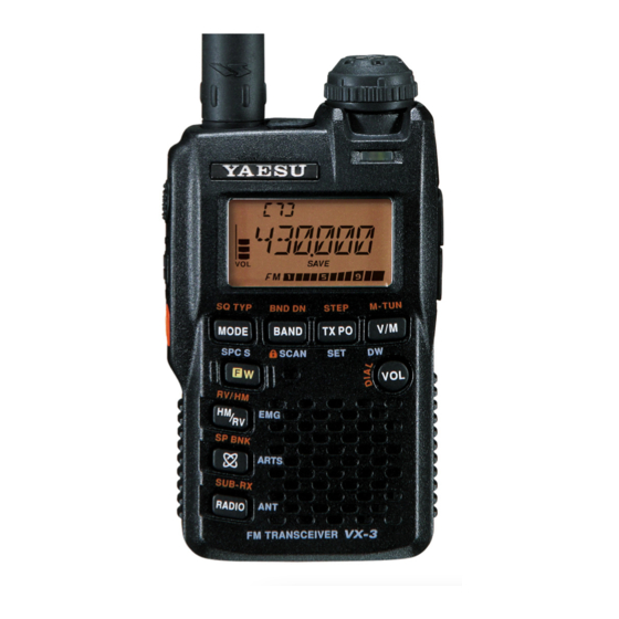
VX-3R/E
Technical Supplement
©2010 VERTEX STANDARD CO., LTD.
This transceiver was assembled using Pb (lead) free solder, based on the RoHS specification.
Only lead-free solder (Alloy Composition: Sn-3.0Ag-0.5Cu) should be used for repairs performed on this appara-
tus. The solder stated above utilizes the alloy composition required for compliance with the lead-free specification,
and any solder with the above alloy composition may be used.
Specification .............................................................................................................................................2
Exploded View & Miscellaneous Parts ..............................................................................................4
Block Diagram .........................................................................................................................................5
Circuit Description.................................................................................................................................7
Alignment .................................................................................................................................................9
Board Unit (Schematics, Layouts & Parts)
MAIN Unit ....................................................................................................................................................................... 15
Filter Unit ......................................................................................................................................................................... 45
SW Unit ............................................................................................................................................................................. 49
VCO Unit .......................................................................................................................................................................... 57
EH028M90D
This manual provides the technical information necessary for servicing the VX-3R/E
Ultra-Compact Dual-Band Transceiver.
Servicing this equipment requires expertise in handing surface-mount chip components.
Attempts by non-qualified persons to service this equipment may result in permanent
damage not covered by the warranty, and may be illegal in some countries.
Two PCB layout diagrams provided for each double-sided board in this transceiver.
Each side of the board is referred to by the type of the majority of components installed
on that side ("Side A" or "Side B"). In most cases one side has only chip components,
and the other has either a mixture of both chip and leaded components (trimmers, coils,
electrolytic capacitors, ICs, etc.), or leaded components only.
While we believe the information in this manual to be correct, VERTEX STANDARD
assumes no liability for damage that may occur as a result of typographical or other
errors that may be present. Your cooperation in pointing out any inconsistencies in the
technical information would be appreciated.
Important Note
Contents
VERTEX STANDARD CO., LTD.
4-8-8 Nakameguro, Meguro-Ku, Tokyo 153-8644, Japan
VERTEX STANDARD
US Headquarters
10900 Walker Street, Cypress, CA 90630, U.S.A.
YAESU UK LTD.
Unit 12, Sun Valley Business Park, Winnall Close
Winchester, Hampshire, SO23 0LB, U.K.
VERTEX STANDARD HK LTD.
Unit 5, 20/F., Seaview Centre, 139-141 Hoi Bun Road,
Kwun Tong, Kowloon, Hong Kong
VERTEX STANDARD AUSTRALIA PTY., LTD.
Normanby Business Park, Unit 14/45 Normanby Road
Notting Hill 3168, Victoria, Australia
1
Advertisement
Table of Contents

Related Manuals for Vertex VX-3R/E


Summary of Contents for Vertex VX-3R/E
-
Page 1: Table Of Contents
(trimmers, coils, electrolytic capacitors, ICs, etc.), or leaded components only. While we believe the information in this manual to be correct, VERTEX STANDARD assumes no liability for damage that may occur as a result of typographical or other errors that may be present. -
Page 2: Specification
Specifications General Frequency Ranges: RX 0.5-1.8 MHz (AM Broadcast) (USA Version) 1.8-30 MHz (SW Band) 30-76 MHz (50 MHz HAM) 76-108 MHz (FM Broadcast) 108-137 MHz (Air Band) 137-174 MHz (144 MHz HAM) 174-222 MHz (VHF TV) 222-420 MHz (GEN1) 420-470 MHz (430 MHz HAM) 470-800(729) MHz (UHF TV) (757-774) MHz (UHF TV) - Page 3 Specifications Receiver Circuit Type: AM, NFM: Double-Conversion Superheterodyne WFM: Triple-Conversion Superheterodyne AM Radio/FM Radio: Single-Conversion Superheterodyne Intermediate Frequencies: 1st: 47.25 MHz (AM, NFM) 1st: 45.8 MHz (WFM) 1st: 130 kHz (AM Broadcast/FM Broadcast) 2nd: 450 kHz (AM, NFM) 2nd: 10.7 MHz (WFM) 3rd: 1 MHz (WFM) Sensitivity: 3 µV for 10 dB SN (0.5-1.8 MHz, AM Broadcast)
-
Page 4: Exploded View & Miscellaneous Parts
Exploded View & Miscellaneous Parts RA0951900 NAME PLATE (YAESU) RA095220B CASE ASSY RA0111400 RA0503600 LATCH NAIL RING NUT RA0689600 RA0947300 WASHER ENCODER KNOB ASSY M3290048 MICROPHONE ELEMENT ’ RA094660B RA094680B RUBBER KNOB (PTT) MIC CAP RA0952300 RA0023500 KEY PAD RING NUT(SMA) M4090159 SPEAKER 0.5W/8-OHM VXSTD P/N... -
Page 5: Block Diagram
Block Diagram... - Page 6 Note...
-
Page 7: Circuit Description
Circuit Description The VX-3R/E consists of a MAIN-UNIT, a FILTER-UNIT, The 47.25 MHz intermediate frequency product of the a SW-UNIT, and a VCO-UNIT. The MAIN-UNIT contains mixer is delivered to the IF circuit. the receiver front end, PLL IC, power and switching cir-... - Page 8 Circuit Description (2) Modulation PLL Frequency Synthesizer Voice signal input from either built-in microphone PLL IC Q1041 (MB15A01PFV1) on the MAIN-UNIT con- MC1001 on MAIN-UNIT or external jack J1004 on the sists of a data shift register, reference frequency divider, MAIN-UNIT is pre-emphasized by C1056 and R1033, and phase comparator, charge pump, intermittent operation processed by microphone amplifier Q1010 (NJM3403AV),...
-
Page 9: Alignment
Alignment Introduction Required Test Equipment The VX-3R/E is carefully aligned at the factory for the RF Signal Generator with calibrated output level at 500 MHz specified performance across the amateur band. Realign- Deviation Meter (linear detector) ment should therefore not be necessary except in the event In-line Wattmeter with 5% accuracy at 500 MHz of a component failure. - Page 10 Alignment Internal System Alignment Routine PLL Reference Frequency Adjustment (REF) This uses a programmed routine in the transceiver, which Rotate the DIAL knob to select the alignment item "rEF". simplifies many previously complex discrete component Press the [V/M] key. settings and adjustments with digitally controlled settings Press the PTT switch, then rotate the DIAL knob so that via front panel buttons and LCD indications.
- Page 11 Alignment NFM S-Meter Full Scale Adjustment Low TX Power Adjustment Connect the RF Signal Generator to the ANT jack, and then Connect the 50-Ohm Dummy Load and Wattmeter to the set the output level to +20 dBµV at the 435.100 MHz (with 1 ANT jack.
- Page 12 Alignment 50 MHz band WFM S-Meter S-1 Adjustment Connect the RF Signal Generator to the ANT jack, and Press the [BAND] button to switch the alignment band to then set the output level to +8 dBµV at the 52.100 MHz 50 MHz Band.
- Page 13 Alignment 144 MHz Band NFM S-Meter Full Scale Adjustment Press the [BAND] button to switch the alignment band to Connect the RF Signal Generator to the ANT jack, and 144 MHz Band. then set the output level to +20 dBµV at the 145.100 MHz RX Tune Adjustment (with 1 kHz tone @ ±3.5 kHz deviation).
- Page 14 Alignment Low TX Power Adjustment CTCSS Tone Deviation Adjustment Connect the 50-Ohm Dummy Load and Wattmeter to Connect the 50-Ohm Dummy Load, Wattmeter, and the ANT jack. Deviation Meter to the ANT jack. Rotate the DIAL knob one click clockwise to select the Rotate the DIAL knob one click clockwise to select the alignment item "LP".
-
Page 15: Main Unit
MAIN Unit (Lot. 1 ~ 3) Circuit Diagram... - Page 16 MAIN Unit (Lot. 1 ~ 3) Note...
- Page 17 MAIN Unit (Lot. 1 ~ 3) Parts Layout (Side A) HD64F2266TF13V LC75834W LV24100LP (Q1095) (Q1100) (Q1014) M62364FP NJM2151AV NJM3403AV AT24C256 (Q1017) (Q1005) (Q1010) (Q1094) NJM12904R (Q1023) 2SK3541 2SA2029 (F*) 2SC5374 (NA) DTA114TE (94) DTA144EM (16) (Q1006, 1007, 1008, (Q1057, 1071, 1073, (Q1077) (Q1039, 1042, 1043) (Q1039, 1042, 1043)
- Page 18 MAIN Unit (Lot. 1 ~ 3) Parts Layout (Side B) NJM2552V MB15A02PFV1 MM1438BWLE (Q1047) (Q1041) (Q1097) 2SJ364 (4M) 2SC4915-O (QY) CPH6102 (AB) DTC144EM (26) (Q1068) (Q1029, 1030, 1033, 1034, (Q1096) (Q1049, 1067, 1098) 1035, 1036, 1037) 2SC5374 (NA) (Q1038, 1048, 1056) 2SC5555ZD (ZD-) (Q1002, 1003, 1013, 1015, 1019, 1020, 1021)
- Page 19 MAIN Unit (Lot. 4 ~7) / AMP Unit (Lot. 5 ~ 7) Circuit Diagram...
- Page 20 MAIN Unit (Lot. 4 ~7) / AMP Unit (Lot. 5 ~ 7) Note...
- Page 21 MAIN Unit (Lot. 4 ~7) / AMP Unit (Lot. 5 ~ 7) Parts Layout (Side A) HD64F2266TF13V LC75834W LV24100LP M62364FP NJM2151AV (Q1095) (Q1100) (Q1014) (Q1017) (Q1005) NJM3403AV AT24C256 2SK3541 2SA2029 (F*) 2SC5374 (NA) (Q1010) (Q1094) (Q1006, 1007, 1008, (Q1057, 1071, 1073, (Q1077) 1016, 1032, 1082) 1092)
- Page 22 MAIN Unit (Lot. 4 ~7) / AMP Unit (Lot. 5 ~7) Parts Layout (Side B) NJM2552V MB15A02PFV1 MM1438BWLE (Q1047) (Q1041) (Q1097) 2SJ364 (4M) 2SC4915-O (QY) CPH6102 (AB) DTC144EM (26) (Q1068) (Q1029, 1030, 1033, 1034, (Q1096) (Q1049, 1067, 1098) 1035, 1036, 1037) 2SC5374 (NA) (Q1038, 1048, 1056) 2SC5555ZD (ZD-)
- Page 23 MAIN Unit (Lot. 8 ~ 12) Circuit Diagram...
- Page 24 MAIN Unit (Lot. 8 ~ 12) Note...
- Page 25 MAIN Unit (Lot. 8 ~ 12) MAIN Unit Parts Layout (Side A) HD64F2266TF13V LC75834W LV24100LP (Q1095) (Q1100) (Q1014) M62364FP NJM2151AV NJM3403AV AT24C256 (Q1017) (Q1005) (Q1010) (Q1094) NJM12904R (Q1023) 2SK3541 2SA2029 (F*) 2SC5374 (NA) DTA114TE (94) DTA144EM (16) (Q1006, 1007, 1008, (Q1057, 1071, 1073, (Q1077) (Q1039, 1042, 1043)
- Page 26 MAIN Unit (Lot. 8 ~ 12) MAIN Unit Parts Layout (Side B) NJM2552V MB15A02PFV1 MM1438BWLE (Q1047) (Q1041) (Q1097) 2SJ364 (4M) 2SC4915-O (QY) CPH6102 (AB) DTC144EM (26) (Q1068) (Q1029, 1030, 1033, 1034, (Q1096) (Q1049, 1067, 1098) 1035, 1036, 1037) 2SC5374 (NA) (Q1038, 1048, 1056) 2SC5555ZD (ZD-) (Q1002, 1003, 1013, 1015,...
- Page 27 MAIN Unit (Lot. 13 ~) Circuit Diagram...
- Page 28 MAIN Unit (Lot. 13 ~) Note...
- Page 29 MAIN Unit (Lot. 13 ~) Parts Layout (Side A) HD64F2266TF13V LC75834W LV24100LP (Q1095) (Q1100) (Q1014) M62364FP NJM2151AV NJM3403AV AT24C256 (Q1017) (Q1005) (Q1010) (Q1094) NJM12904R (Q1023) 2SK3541 2SA2029 (F*) 2SC5374 (NA) DTA114TE (94) DTA144EM (16) (Q1006, 1007, 1008, (Q1057, 1071, 1073, (Q1077) (Q1039, 1042, 1043) (Q1039, 1042, 1043)
- Page 30 MAIN Unit (Lot. 13 ~) Parts Layout (Side B) NJM2552V MB15A02PFV1 MM1438BWLE (Q1047) (Q1041) (Q1097) 2SJ364 (4M) 2SC4915-O (QY) CPH6102 (AB) DTC144EM (26) (Q1068) (Q1029, 1030, 1033, 1034, (Q1096) (Q1049, 1067, 1098) 1035, 1036, 1037) 2SC5374 (NA) (Q1038, 1048, 1056) 2SC5555ZD (ZD-) (Q1002, 1003, 1013, 1015, 1019, 1020, 1021)
- Page 31 Main Unit Parts List DESCRIPTION VALUE TOL. MFR'S DESIG VXSTD P/N VERS. LOT SIDE LAY ADR P.C.B. with Components (W/ SW Unit, VCO Unit) CS1943001 DST:USA TYP:A2U P.C.B. with Components (W/ SW Unit, VCO Unit) CS1943003 DST:EXP TYP:A1 P.C.B. with Components (W/ SW Unit, VCO Unit) CS1943004 DST:EXP TYP:A2...
- Page 32 Main Unit Parts List DESCRIPTION VALUE TOL. MFR'S DESIG VXSTD P/N VERS. LOT SIDE LAY ADR C 1054 CHIP CAP. 6.3V GRM155B30J105KE18D K22088803 C 1055 CHIP CAP. 0.001uF UMK105B102KW-F K22178829 C 1056 CHIP CAP. 0.0047uF TMK105B472KW-F K22148831 C 1057 CHIP CAP. 0.001uF UMK105B102KW-F K22178829...
- Page 33 Main Unit Parts List DESCRIPTION VALUE TOL. MFR'S DESIG VXSTD P/N VERS. LOT SIDE LAY ADR C 1113 CHIP CAP. 0.01uF GRM36B103K16PT K22128804 C 1113 CHIP CAP. 0.01uF GRM155B11E103KA01D K22148834 C 1114 CHIP CAP. 0.001uF UMK105B102KW-F K22178829 C 1115 CHIP CAP. 0.01uF GRM36B103K16PT K22128804...
- Page 34 Main Unit Parts List DESCRIPTION VALUE TOL. MFR'S DESIG VXSTD P/N VERS. LOT SIDE LAY ADR C 1163 CHIP CAP. 100pF UMK105CH101JV-F K22178282 C 1164 CHIP CAP. 100pF UMK105CH101JV-F K22178282 C 1165 CHIP CAP. 10pF UMK105CH100DV-F K22178258 C 1166 CHIP CAP. 0.1uF GRM155B11A104KA01D K22108802...
- Page 35 Main Unit Parts List DESCRIPTION VALUE TOL. MFR'S DESIG VXSTD P/N VERS. LOT SIDE LAY ADR C 1245 CHIP CAP. 15pF GRM1552C1H150JZ01D K22178216 C 1246 CHIP CAP. 15pF GRM1552C1H150JZ01D K22178216 C 1247 CHIP CAP. UMK105CH050CV-F K22178253 C 1247 CHIP CAP. UMK105CJ030CV-F K22178251 C 1248...
- Page 36 Main Unit Parts List DESCRIPTION VALUE TOL. MFR'S DESIG VXSTD P/N VERS. LOT SIDE LAY ADR C 1315 CHIP CAP. UMK105CH080DV-F K22178256 C 1316 CHIP CAP. 0.001uF UMK105B102KW-F K22178829 C 1318 CHIP CAP. 100pF GRM1552C1H101JD01D K22178236 C 1319 CHIP CAP. 0.047uF GRM155F11C473ZA01D K22129004...
- Page 37 Main Unit Parts List DESCRIPTION VALUE TOL. MFR'S DESIG VXSTD P/N VERS. LOT SIDE LAY ADR D 1012 DIODE 1SV325(TPH3.F) G2070848 D 1013 DIODE HVC369B TRF-E G2070872 D 1014 DIODE 1SV325(TPH3.F) G2070848 D 1015 DIODE 1SV325(TPH3.F) G2070848 D 1016 DIODE HVC369B TRF-E G2070872 D 1017...
- Page 38 Main Unit Parts List DESCRIPTION VALUE TOL. MFR'S DESIG VXSTD P/N VERS. LOT SIDE LAY ADR J 1004 CONNECTOR MJC-046-C1-3.5-T P1091309 J 1005 CONNECTOR AXK6F10345YP P0091378 J 1006 CONNECTOR AXK6F10345YP P0091378 J 1007 CONNECTOR AXK6F10345YP P0091378 J 1009 CONNECTOR MJC-051-A1-1-T P1091311 L 1001 M.RFC...
- Page 39 Main Unit Parts List DESCRIPTION VALUE TOL. MFR'S DESIG VXSTD P/N VERS. LOT SIDE LAY ADR Q 1012 TRANSISTOR MT3S36FS(TE85L.F) G3070377 Q 1013 TRANSISTOR 2SC5555ZD-TR G3355557 Q 1014 LV24100LP-TLM-E G1094371 Q 1015 TRANSISTOR 2SC5555ZD-TR G3355557 Q 1016 2SK3541 T2L G3835417 Q 1017 M62364FP 600D G1093033...
- Page 40 Main Unit Parts List DESCRIPTION VALUE TOL. MFR'S DESIG VXSTD P/N VERS. LOT SIDE LAY ADR Q 1102 TRANSISTOR DTC144EM T2L G3070309 Q 1103 SSM6J25FE(TAPE) G3070379 Q 1104 TRANSISTOR DTC144EM T2L G3070309 Q 1105 TRANSISTOR DTC144EM T2L G3070309 Q 1106 TRANSISTOR 2SC5374-TL G3353748...
- Page 41 Main Unit Parts List DESCRIPTION VALUE TOL. MFR'S DESIG VXSTD P/N VERS. LOT SIDE LAY ADR R 1067 CHIP RES. 1/16W RMC1/16S 221JTH J24189017 R 1068 CHIP RES. 270k 1/16W RMC1/16S 274JTH J24189054 R 1068 CHIP RES. 330k 1/16W RMC1/16S 334JTH J24189055 R 1069 CHIP RES.
- Page 42 Main Unit Parts List DESCRIPTION VALUE TOL. MFR'S DESIG VXSTD P/N VERS. LOT SIDE LAY ADR R 1136 CHIP RES. 1/16W RMC1/16S 102JTH J24189025 R 1137 CHIP RES. 1/16W RMC1/16S 103JTH J24189037 R 1138 CHIP RES. 1/16W RMC1/16S 333JTH J24189043 R 1139 CHIP RES.
- Page 43 Main Unit Parts List DESCRIPTION VALUE TOL. MFR'S DESIG VXSTD P/N VERS. LOT SIDE LAY ADR R 1237 CHIP RES. 1/16W RMC1/16S 223JTH J24189041 R 1238 CHIP RES. 1/16W RMC1/16S 223JTH J24189041 R 1239 CHIP RES. 2.7k 1/16W RMC1/16S 272JTH J24189030 R 1240 CHIP RES.
- Page 44 Main Unit/AMP Unit DESCRIPTION VALUE TOL. MFR'S DESIG VXSTD P/N VERS. LOT SIDE LAY ADR S 1005 TACT SWITCH SKRWAEE030 N5090156 S 1006 TACT SWITCH SKRWAEE030 N5090156 S 1007 TACT SWITCH SKRWAEE030 N5090156 S 1008 TACT SWITCH SKRWAEE030 N5090156 S 1009 TACT SWITCH SKRWAEE030 N5090156...
-
Page 45: Filter Unit
Filter Unit Circuit Diagram... - Page 46 Filter Unit Parts Layout (Side A) DA221M (K) (D2002) DAN222M (N) (D2001) LM2902PWR LM2904PWR 2SC5658 (B*) DTC144EM (26) DTC144TEM (96) (Q2001) (Q2002) (Q2003) (Q2004, 2005, (Q2006) 2007, 2008) Parts Layout (Side B)
- Page 47 Filter Unit Parts List DESCRIPTION VALUE TOL. MFR'S DESIG VXSTD P/N VERS. LOT SIDE LAY ADR P.C.B. with Components CB4006001 Printed Circuit Board FR016770C C 2001 CHIP CAP. 6.3V GRM155B30J105KE18D K22088803 C 2002 CHIP CAP. 0.0047uF TMK105B472KW-F K22148831 C 2003 CHIP CAP.
- Page 48 Filter Unit Note...
-
Page 49: Sw Unit
SW Unit (Lot. 1 ~ 3) Circuit Diagram... - Page 50 SW Unit (Lot. 1 ~ 3) Parts Layout (Side A) RQA0003DNS (Q3004) Parts Layout (Side B) 2SC5226 (R22) DTC143ZE (E23) (Q3003) (Q3003) 2SC5374 (NA) (Q3001)
- Page 51 SW Unit (Lot. 4 ~ 7) Circuit Diagram...
- Page 52 SW Unit (Lot. 4 ~ 7) Parts Layout (Side A) RQA0003DNS (Q3004) Parts Layout (Side B) 2SC5226 (R22) DTC143ZE (E23) (Q3003) (Q3003) 2SC5374 (NA) (Q3001)
- Page 53 SW Unit (Lot. 8 ~) Circuit Diagram...
- Page 54 SW Unit (Lot. 8 ~) Parts Layout (Side A) RQA0003DNS (Q3004) Parts Layout (Side B) 2SC5226 (R22) DTC143ZE (E23) (Q3003) (Q3003) 2SC5374 (NA) (Q3001)
- Page 55 SW Unit Parts List DESCRIPTION VALUE TOL. MFR'S DESIG VXSTD P/N VERS. LOT SIDE LAY ADR P.C.B. with Components CS1944003 DST:USA P.C.B. with Components CS1944004 DST:EXP P.C.B. with Components CS1944005 DST:EU P.C.B. with Components CS1944006 DST:AUS Printed Circuit Board FR016510D Printed Circuit Board FR016510E Printed Circuit Board...
- Page 56 SW Unit Parts List DESCRIPTION VALUE TOL. MFR'S DESIG VXSTD P/N VERS. LOT SIDE LAY ADR R 3002 CHIP RES. 1/16W RMC1/16S 103JTH J24189037 EUROPE R 3002 CHIP RES. 1/16W RMC1/16S 103JTH J24189037 EXPORT R 3002 CHIP RES. 8.2k 1/16W RMC1/16S 822JTH J24189036 R 3004...
-
Page 57: Vco Unit
VCO Unit (Lot. 1 ~ 4) Circuit Diagram... - Page 58 VCO Unit (Lot. 1 ~ 4) Parts Layout (Side A) DTC143ZE (E23) (Q4001, 4003, 4007) MT3S36FS (21) (Q4002, 4004, 4005, 4006) Parts Layout (Side B)
- Page 59 VCO Unit (Lot. 5 ~) Circuit Diagram...
- Page 60 VCO Unit (Lot. 5 ~) Parts Layout (Side A) DTC143ZE (E23) (Q4001, 4003, 4007) MT3S36FS (21) (Q4002, 4004, 4005, 4006) Parts Layout (Side B)
- Page 61 VCO Unit (Lot. 54 ~) Circuit Diagram...
- Page 62 VCO Unit (Lot. 54 ~) Parts Layout (Side A) DTC143ZE (E23) (Q4001, 4003, 4007) MT3S36FS (21) (Q4002, 4004, 4005, 4006) Parts Layout (Side B)
- Page 63 VCO Unit Parts List DESCRIPTION VALUE TOL. MFR'S DESIG VXSTD P/N VERS. LOT SIDE LAY ADR P.C.B. with Components CB3815001 Printed Circuit Board FR015870A Printed Circuit Board FR015870B Printed Circuit Board FR015870C C 4001 CHIP CAP. 0.001uF UMK105B102KW-F K22178829 C 4002 CHIP CAP.
- Page 64 VCO Unit Parts List DESCRIPTION VALUE TOL. MFR'S DESIG VXSTD P/N VERS. LOT SIDE LAY ADR D 4015 DIODE 1SV325(TPH3.F) G2070848 J 4001 CONNECTOR AXK5F10335YP P1091136 J 4002 CONNECTOR AXK5F10335YP P1091136 L 4001 M.RFC LK1608 1R0K-T L1690687 L 4002 M.RFC 0.0082uH C1608CB-8N2G-RF L1691226...
- Page 66 Copyright 2010 VERTEX STANDARD CO., LTD. All rights reserved No portion of this manual may be reproduced without the permission of VERTEX STANDARD CO., LTD.
Need help?
Do you have a question about the VX-3R/E and is the answer not in the manual?
Questions and answers