Table of Contents
Advertisement
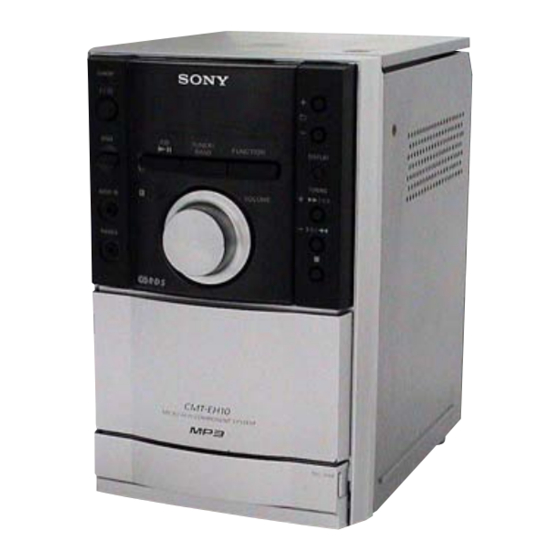
SERVICE MANUAL
Ver. 1.4 2006.03
• HCD-EH10 is the amplifier, CD player, tape deck and
tuner section in CMT-EH10.
Main unit
AUDIO POWER SPECIFICATIONS
POWER OUTPUT AND TOTAL HARMONIC DISTORTION:
(The United States model only)
With 4 ohm loads, both channels driven, from 100 – 20,000 Hz; rated 4 watts per channel
minimum RMS power, with no more than 10% total harmonic distortion from 250 milliwatts to
rated output.
Amplifier section
North-American model:
Continuous RMS power output (reference): 5 + 5 W (4 ohms at 1 kHz, 10% THD)
European model:
DIN power output (rated): 4 + 4 W (4 ohms at 1 kHz, DIN)
Continuous RMS power output (reference): 5 + 5 W (4 ohms at 1 kHz, 10% THD)
Music power output (reference): 7 + 7 W
The following are measured at AC 240 V, 50/60 Hz (Australian model), AC 220 V, 60 Hz (Korean
model), AC 120 V, 50/60 Hz (Taiwanese model), AC 120 or 240 V, 50/60 Hz (other models)
DIN power output (rated): 4 + 4 W (4 ohms at 1 kHz, DIN)
Continuous RMS power output (reference): 5 + 5 W (4 ohms at 1 kHz, 10% THD)
Inputs
AUDIO IN (stereo mini jack): Sensitivity 800 mV, impedance 47 kilohms
Outputs
PHONES (stereo mini jack): Accepts headphones with an impedance of 8 ohms or more
SPEAKER: Accepts impedance of 4 ohms
CD player section
System: Compact disc and digital audio system
Laser Diode Properties
Emission duration: continuous
Laser Output*: Less than 44.6µ W
* This output is the value measurement at a distance of 200mm from the objective lens surface
on the Optical Pick-up Block with 7mm aperture.
Frequency response: 20 Hz – 20 kHz
Signal-to-noise ratio: More than 90 dB
Dynamic range: More than 90 dB
Tape deck section
Recording system: 4-track 2-channel, stereo
Sony Corporation
9-879-855-05
Personal Audio Division
2006C05-1
Published by Sony Techno Create Corporation
© 2006.03
HCD-EH10
Model Name Using Similar Mechanism
CD Section
Base Unit Name
Optical Pick-up Name
Model Name Using Similar Mechanism
TAPE Section
Tape Transport Mechanism Type
SPECIFICATIONS
Tuner section
FM stereo, FM/AM superheterodyne tuner
Antenna:
FM lead antenna
AM loop antenna
FM tuner section:
Tuning range
North American model: 87.5 – 108.0 MHz (100 kHz step)
Other models: 87.5 – 108.0 MHz (50 kHz step)
Intermediate frequency: 10.7 MHz
AM tuner section:
Tuning range
North American models: 530 – 1,710 kHz (with 10 kHz tuning interval)
European model: 531 – 1,602 kHz (with 9 kHz tuning interval)
Other models: 530 – 1,710 kHz (with 10 kHz tuning interval)
Intermediate frequency: 450 kHz
General
Power requirements
North American model: AC 120 V, 60 Hz
European model: AC 230 V, 50/60 Hz
Australian model: AC 230 – 240 V, 50/60 Hz
Korean model: AC 220 V, 60 Hz
Taiwanese model: AC 120 V, 50/60 Hz
Other models: AC 110 – 120 or 220 – 240 V, 50/60 Hz
Adjustable with voltage selector
Power consumption:
North American model: 23 W
European model: 22 W
Other models: 22 W
Dimensions (w/h/d) (excl. speakers): Approx. 158 × 241.5 × 233 mm
Mass (excl. speakers):
Approx. 2.1 kg
Supplied accessories: Remote Commander (1)/FM/AM antenna (1)
Design and specifications are subject to change without notice.
COMPACT DISC DECK RECEIVER
Canadian Model
AEP Model
Australian Model
NEW
BU-K8BD83S-WOD
KSM-213CDP
NEW
H-21SB
531 – 1,710 kHz (with 9 kHz tuning interval)
531 – 1,602 kHz (with 9 kHz tuning interval)
1.0 W (in Power off)
US Model
UK Model
E Model
Advertisement
Table of Contents

Related Manuals for Sony HCD-EH10


Summary of Contents for Sony HCD-EH10
-
Page 1: Specifications
Canadian Model Ver. 1.4 2006.03 AEP Model UK Model E Model Australian Model • HCD-EH10 is the amplifier, CD player, tape deck and tuner section in CMT-EH10. Model Name Using Similar Mechanism CD Section Base Unit Name BU-K8BD83S-WOD Optical Pick-up Name... -
Page 2: Table Of Contents
LES DIAGRAMMES SCHÉMATIQUES ET LA LISTE DES PIÈCES SONT CRITIQUES POUR LA SÉCURITÉ DE FONCTIONNEMENT. NE REMPLACER CES COM- POSANTS QUE PAR DES PIÈCES SONY DONT LES NUMÉROS SONT Earth Ground DONNÉS DANS CE MANUEL OU DANS LES SUPPLÉMENTS PUBLIÉS PAR SONY. -
Page 3: Servicing Notes
HCD-EH10 Ver. 1.4 SECTION 1 SERVICING NOTES UNLEADED SOLDER NOTES ON HANDLING THE OPTICAL PICK-UP Boards requiring use of unleaded solder are printed with the lead- BLOCK OR BASE UNIT free mark (LF) indicating the solder contains no lead. The laser diode in the optical pick-up block may suffer electrostatic... -
Page 4: General
HCD-EH10 SECTION 2 This section is extracted from instruction manual. GENERAL... - Page 5 HCD-EH10...
-
Page 6: Disassembly
HCD-EH10 SECTION 3 DISASSEMBLY • This set can be disassembled in the order shown below. 3-1. DISASSEMBLY FLOW 3-2. REAR CABINET SECTION (Page 6) 3-3. FRONT CABINET SECTION, TOP CABINET SECTION AND MAIN BOARD (Page 7) 3-5. BASE UNIT SECTION 3-4. -
Page 7: Front Cabinet Section, Top Cabinet Section And Main Board
HCD-EH10 3-3. FRONT CABINET SECTION, TOP CABINET SECTION AND MAIN BOARD 9 top cabinet section claw claw 8 two screws 2 connector (B2.6) (SW750) q; MAIN board 4 claw 6 flexible flat (23 core) cable (FFC151) (CNS104) 7 lead wire (PIN102) -
Page 8: Base Unit Section (Bu-K8Bd83S-Wod)
HCD-EH10 3-5. BASE UNIT SECTION (BU-K8BD83S-WOD) 7 CD cover 6 two claws 4 vibration proof rubber (red) 6 two claws 8 base unit sction (BU-K8BD83S-WOD) 5 vibration proof rubber (green) 4 vibration proof rubber (red) 2 two screws 2 two screws (PWH B2.6) -
Page 9: Test Mode
HCD-EH10 SECTION 4 TEST MODE COLD RESET CD POWER MANEGE * The cold reset clears all data including preset data stored in * This mode is for switch the CD power supply on/off. Even if the RAM to initial conditions. Execute this mode when this state pulls out AC plug, it is held. -
Page 10: Mechanical Adjustments
HCD-EH10 Ver. 1.1 SECTION 5 SECTION 6 MECHANICAL ADJUSTMENTS ELECTRICAL ADJUSTMENTS • Precaution 0 dB=1 µV TUNER SECTION 1. Clean the following parts with a denatured-alcohol-moistened swab : [AM (MW/LW)] record/playback head pinch roller Setting: erase head rubber belts Function : TUNER... - Page 11 HCD-EH10 FM TRACKING ADJUSTMENT Adjustment Location: Adjust for a maximum reading on level meter L804 98 MHz – MAIN Board (Component Side) – FM DETECTOR ADJUSTMENT Setting: Function: TUNER BAND button: FM FM RF Signal generator MAIN board JW403 (TUNER OUT L-ch)
- Page 12 HCD-EH10 4. After the adjustments, apply suitable locking compound to DECK SECTION 0 dB=0.775 V the pats adjusted. 1. Demagnetize the record/playback head with a head Adjustment Location: Record/Playback/Erase Head demagnetizer. – When there is a hole for the azimuth adjustment –...
- Page 13 HCD-EH10 CD SECTION Note: 1. CD Block is basically constructed to operate without adjustment. 2. Use YEDS-18 disc (3-702-101-01) unless otherwise indicated. 3. Use an oscilloscope with more than 10 MW impedance. 4. Clean the object lens by an applicator with neutral detergent when the signal level is low than specified value with the following checks.
-
Page 14: Diagrams
HCD-EH10 SECTION 7 DIAGRAMS 7-1. BLOCK DIAGRAM – CD SERVO Section – OPTICAL PICK-UP BLOCK (KSM-213CDP) RFACO RFACI (Page 16) AOUT1 112 AOUT2 117 R-CH XTAI 109 AUTOMATIC X201 POWER CONTROL 16.9344MHz Q321 XTAO 108 • R-ch is omitted due to same as L-ch. -
Page 15: Block Diagram - Tuner Section
HCD-EH10 Ver. 1.3 7-2. BLOCK DIAGRAM – TUNER Section – CNP802 ANTENNA FM/AM (AEP, UK, East European, Russian) BAND-PASS FM MIX CF801 CF802 TUNER (Page 16) FILTER 36 FMRF-IN FM-MIX 8 FMIF-IN FMDET-OUT 22 MPX-IN L-OUT Q803 BPF801 R-OUT R-CH... -
Page 16: Block Diagram - Main Section
HCD-EH10 Ver. 1.3 7-3. BLOCK DIAGRAM – MAIN Section – J105 R-CH 19 A1 AUDIO IN OUT1 POWER J102 • R-ch is omitted due to same as L-ch. PHONES • SIGNAL PATH (Page 14) IC301 23 C1 R-CH : TUNER... - Page 17 HCD-EH10 Ver. 1.4 • Note for Printed Wiring Boards and Schematic Diagrams • Waveforms – CD Board – – MAIN Board – – PANEL Board – Note on Printed Wiring Board: Note on Schematic Diagram: • X : parts extracted from the component side.
-
Page 18: Printed Wiring Board - Cd Board
HCD-EH10 Ver. 1.4 • See page 17 for Circuit Boards Location. 7-4. PRINTED WIRING BOARD – CD Board – : Uses unleaded solder. M401 (SPINDLE) CD BOARD (COMPONENT SIDE) CD BOARD (CONDUCTOR SIDE) S201 (LIMIT) R280 C405 C406 R451 M402... -
Page 19: Schematic Diagram - Cd Board
HCD-EH10 Ver. 1.4 • See page 17 for Waveforms. • See page 26 for IC Block Diagrams. • See page 31 for IC Pin Function Description. 7-5. SCHEMATIC DIAGRAM – CD Board – C210 C208 (RFACI) C230 R256 100p C257... -
Page 20: Printed Wiring Boards - Main Section
HCD-EH10 Ver. 1.4 • See page 17 for Circuit Boards Location. 7-6. PRINTED WIRING BOARDS – MAIN Section – : Uses unleaded solder. • Semiconductor Location (Page 18) (Page 24) CD BOARD PANEL BOARD MAIN BOARD Ref. No. Location CN102... -
Page 21: Schematic Diagram - Main Section (1/3)
HCD-EH10 Ver. 1.4 7-7. SCHEMATIC DIAGRAM – MAIN Section (1/3) – (1/3) CNP501 HRP501 (REC/PB) R-CH L-CH JW107 CNP502 SW501 (REC/PB) TAPE RDSC RDS-CLK MECHANISM RDSD (Page 22) C535 DECK RDS-DO TUAS CNS112 TU-ANSD TUDO TU-DO TUDI RDSC I-RDS-SC TU-DI... -
Page 22: Schematic Diagram - Main Section (2/3)
HCD-EH10 Ver. 1.4 • See page 26 for IC Block Diagrams. 7-8. SCHEMATIC DIAGRAM – MAIN Section (2/3) – (Page 21) (2/3) C532 1000p (Page 21) R406 C531 C403 C515 1000p C509 VM9V R410 R404 33 16V 100k TU-L R412... -
Page 23: Schematic Diagram - Main Section (3/3)
HCD-EH10 Ver. 1.4 • See page 17 for Waveforms. • See page 26 for IC Block Diagrams. 7-9. SCHEMATIC DIAGRAM – MAIN Section (3/3) – (3/3) R857 R862 C868 C869 D851 SVC347A C855 470p R865 L851 L852 JR861 C862 AM-RF... -
Page 24: Printed Wiring Board - Panel Board
HCD-EH10 Ver. 1.4 • See page 17 for Circuit Boards Location. 7-10. PRINTED WIRING BOARD – PANEL Board – : Uses unleaded solder. • Semiconductor Location Ref. No. Location D701 D702 SW750 CD LID PANEL BOARD OPEN/CLOSE DETECT IC701 IC703... -
Page 25: Schematic Diagram - Panel Board
HCD-EH10 Ver. 1.4 • See page 17 for Waveforms. • See page 31 for IC Pin Function Description. 7-11. SCHEMATIC DIAGRAM – PANEL Board – R775 L702 X702 4.19MHz Q701 R767 2SA1235F D702 220k R713 C703 MC2836 Q701-703 R721 LCD702 +4V REGULATOR 6.3V... - Page 26 HCD-EH10 • IC Block Diagrams – CD Board – IC402 BA5947FM-E2 IC401 BD3881FV MUTING BASS BASS + – INTERFACE LEVEL SHIFT VOLUME TREBLE INTERFACE INTERFACE LOGIC CONTROL VOLUME TREBLE VREF – MAIN Board – IC301 LA4631-E POP NOISE THERMAL REFERENCE...
- Page 27 HCD-EH10 IC801 LV23003VA 36 FM RF-IN AM RF-IN 35 GND2 34 FMRF-OUT 33 VCC2 FM-MIX 32 FM-OSC GND1 AM-MIX 31 AM-OSC VCC1 30 BO2 29 BO1 BUFFER LOW-PASS 28 LP-OUT FILTER 27 LP-IN 26 PD 25 AGC AMIF-IN 24 AMDET-OUT...
- Page 28 HCD-EH10 IC861 PT2579SN OSCILLATION TEST LOGIC & & OUTPUT SELECTOR DIVIDER SWITCH BIPHASE COSTAS LOOP CLOCKED ANTI-ALIASING SYMBOL VARIABLE & COMPARATOR FILTER DECODER FIXED DIVIDER CLOCK 57 kHz REGENERATION BAND PASS & SYNC (8th ORDER) QUALITY BIT DIFFERENTIAL REFERENCE RECONSTRUCTION...
- Page 29 HCD-EH10 • IC PIN FUNCTION DESCRIPITION CD BOARD IC201 CXD3014A-201R (CD DSP) Pin No. Pin Name Description LRCK L/R sampling clock signal output terminal LRCKI L/R sampling clock signal input terminal PCMD Serial data output terminal PCMDI Serial data input terminal...
- Page 30 HCD-EH10 Pin No. Pin Name Description AVDD0 Power supply terminal (+3.3V) AVSS0 Ground terminal E signal input from the optical pick-up block F signal input from the optical pick-up block Tracking error signal input terminal Tracking error signal output terminal...
- Page 31 HCD-EH10 Pin No. Pin Name Description TRST Not used Ground terminal Power supply terminal (+1.8V) IOVDD2 Power supply terminal (+3.3V) DOUT Digital audio signal output terminal Not used TEST Test terminal Normally: fixed at "L" TES1 Test terminal Normally: fixed at "L"...
- Page 32 HCD-EH10 Ver. 1.3 PANEL BOARD IC701 MB90802-107 (SYSTEM CONTROLLER) Pin No. Pin Name Description Main power on/off control signal output terminal "H": on Standby control signal output to the power amplifier and system reset signal output to the CD DSP...
- Page 33 HCD-EH10 Pin No. Pin Name Description serial data transfer clock signal output to the FM/AM tuner Serial data output to the FM/AM tuner Terminal for doubler circuit capacitor connection to develop liquid crystal display drive voltage 59 to 62 COM0 to COM3...
-
Page 34: Exploded Views
HCD-EH10 Ver. 1.4 SECTION 8 EXPLODED VIEWS NOTE: • Items marked “*” are not stocked since they • -XX and -X mean standardized parts, so they The components identified by mark 0 or dotted line with mark 0 are may have some difference from the original are seldom required for routine service. -
Page 35: Front Cabinet Section
HCD-EH10 Ver. 1.4 8-2. FRONT CABINET SECTION FFC701, FFC702 LED701 PANEL board LCD702 supplied supplied not supplied not supplied Ref. No. Part No. Description Remark Ref. No. Part No. Description Remark 2-636-520-01 COVER (C), BUTTON 2-636-545-01 SHEET (LCD) 2-637-768-01 SPRING (CASSETTE) -
Page 36: Top Cabinet Section
HCD-EH10 Ver. 1.3 8-3. TOP CABINET SECTION not supplied SW750 base unit section (BU-K8BD83S-WOD) Ref. No. Part No. Description Remark Ref. No. Part No. Description Remark 2-636-518-01 LID, CD 3-931-379-21 RUBBER, VIBRATION PROOF (RED) 1-452-899-11 MAGNET 3-252-828-01 SCREW (B2.6), (+) PWH TAPPING... -
Page 37: Base Unit Section (Bu-K8Bd83S-Wod)
HCD-EH10 8-4. BASE UNIT SECTION (BU-K8BD83S-WOD) (including sled motor (M402), spindle motor (M401)) included in (spindle motor (M401)) included in (sled motor (M402)) S201 Ref. No. Part No. Description Remark Ref. No. Part No. Description Remark 0 151 8-820-126-01 OPTICAL PICK-UP BLOCK... -
Page 38: Electrical Parts List
HCD-EH10 Ver. 1.4 SECTION 9 ELECTRICAL PARTS LIST NOTE: • Due to standardization, replacements in the • Items marked “*” are not stocked since they The components identified by mark parts list may be different from the parts are seldom required for routine service. - Page 39 HCD-EH10 Ver. 1.3 MAIN Ref. No. Part No. Description Remark Ref. No. Part No. Description Remark < RESISTOR/FERRITE BEAD > < BAND PASS FILTER > R101 1-216-809-11 METAL CHIP 1/10W BPF801 1-236-711-41 FILTER, BAND PASS R102 1-216-809-11 METAL CHIP 1/10W...
- Page 40 HCD-EH10 MAIN Ref. No. Part No. Description Remark Ref. No. Part No. Description Remark C415 1-100-566-91 CERAMIC CHIP 0.1uF C416 1-100-566-91 CERAMIC CHIP 0.1uF C814 1-164-156-11 CERAMIC CHIP 0.1uF C421 1-100-566-91 CERAMIC CHIP 0.1uF C815 1-162-927-11 CERAMIC CHIP 100PF C816 1-115-467-11 CERAMIC CHIP 0.22uF...
- Page 41 HCD-EH10 MAIN Ref. No. Part No. Description Remark Ref. No. Part No. Description Remark < DIODE > < TRANSISTOR > D106 8-719-056-85 DIODE UDZ-TE-17-8.2B Q101 8-729-141-83 TRANSISTOR 2SB1094-LK D107 8-719-046-07 DIODE 2A02M Q102 8-729-120-28 TRANSISTOR 2SC1623-L5L6 D108 8-719-046-07 DIODE 2A02M...
- Page 42 HCD-EH10 MAIN Ref. No. Part No. Description Remark Ref. No. Part No. Description Remark R145 1-216-817-11 METAL CHIP 1/10W R404 1-216-813-11 METAL CHIP 1/10W R146 1-216-817-11 METAL CHIP 1/10W R405 1-216-864-11 SHORT CHIP R147 1-216-817-11 METAL CHIP 1/10W R148 1-216-817-11 METAL CHIP...
- Page 43 HCD-EH10 Ver. 1.4 MAIN PANEL Ref. No. Part No. Description Remark Ref. No. Part No. Description Remark R536 1-216-813-11 METAL CHIP 1/10W R850 1-216-825-11 METAL CHIP 2.2K 1/10W R541 1-216-837-11 METAL CHIP 1/10W R851 1-216-837-11 METAL CHIP 1/10W R542 1-216-833-11 METAL CHIP...
- Page 44 HCD-EH10 Ver. 1.4 PANEL Ref. No. Part No. Description Remark Ref. No. Part No. Description Remark C717 1-162-964-11 CERAMIC CHIP 0.001uF LED702 8-719-060-44 LED SLR-342VRT32 (STANDBY) C718 1-162-964-11 CERAMIC CHIP 0.001uF C719 1-165-176-11 CERAMIC CHIP 0.047uF < TRANSISTOR > C720 1-162-964-11 CERAMIC CHIP 0.001uF...
- Page 45 HCD-EH10 Ver. 1.4 PANEL PT-AC Ref. No. Part No. Description Remark Ref. No. Part No. Description Remark R750 1-216-821-11 METAL CHIP 1/10W X702 1-795-054-51 VIBRATOR, CERAMIC (4.19MHz) ************************************************************ R751 1-216-845-11 METAL CHIP 100K 1/10W R753 1-216-809-11 METAL CHIP 1/10W A-1138-529-A PT-AC BOARD, COMPLETE...
- Page 46 HCD-EH10 MEMO...
- Page 47 HCD-EH10 US Model Canadian Model SERVICE MANUAL AEP Model UK Model E Model Ver. 1.4 2006.03 Australian Model SUPPLEMENT-1 File this supplement with the service manual. Subject: Change of MAIN and PT-AC boards (Suffix-13) In this set, MAIN and PT-AC boards have been changed in the midway of production.
- Page 48 HCD-EH10 Ver. 1.4 DIAGRAMS • Note for Printed Wiring Boards and Schematic Diagrams Note on Schematic Diagram: Note on Printed Wiring Board: • All capacitors are in µF unless otherwise noted. (p: pF) • X : parts extracted from the component side.
- Page 49 HCD-EH10 Ver. 1.4 : Uses unleaded solder. 2-1. PRINTED WIRING BOARDS – MAIN Section – • Semiconductor Location Ref. No. Location CD BOARD PANEL BOARD MAIN BOARD D106 CN102 CNS701 (AEP, UK, EE, RU) CNS702 (US, CND, SP, TW, KR, AUS)
- Page 50 HCD-EH10 Ver. 1.4 2-2. SCHEMATIC DIAGRAM – MAIN Section (1/3) – (1/3) CNP501 HRP501 (REC/PB) R-CH C535 L-CH JW137 (US,CND) JW107 CNP502 SW501 (EXCEPT US,CND) JW137 TAPE (REC/PB) RDSC MECHANISM RDS-CLK DECK RDSD (Page 22) RDS-DO TUAS CNS111 25P(US,CND,SP,TW,KR,AUS) TU-ANSD...
- Page 51 HCD-EH10 2-3. SCHEMATIC DIAGRAM – MAIN Section (2/3) – (Page 4) (2/3) C532 1000p (Page 4) R406 C531 C403 C515 1000p C509 VM9V R410 R404 33 16V 100k TU-L R412 C543 R517 TU-GND 1000p 100k TU-R R411 R403 C421 C503...
- Page 52 HCD-EH10 Ver. 1.4 2-4. SCHEMATIC DIAGRAM – MAIN Section (3/3) – (AEP,UK,EE,RU) (3/3) R857 R862 C868 C869 D851 SVC347A C855 470p R865 L851 L852 JR861 C862 AM-RF AM-LO JW821 R809 R811 R812 (VT) 4.7k R851 R808 R807 R839 R814 C834...
- Page 53 HCD-EH10 Ver. 1.4 AC-SW MAIN ELECTRICAL PARTS LIST NOTE: • Items marked “*” are not stocked since they • Due to standardization, replacements in the The components identified by mark 0 or dotted line with mark 0 are parts list may be different from the parts are seldom required for routine service.
- Page 54 HCD-EH10 Ver. 1.4 MAIN Ref. No. Part No. Description Remark Ref. No. Part No. Description Remark C434 1-162-962-11 CERAMIC CHIP 470PF C818 1-216-864-11 SHORT CHIP C819 1-162-964-11 CERAMIC CHIP 0.001uF C437 1-162-962-11 CERAMIC CHIP 470PF C820 1-162-964-11 CERAMIC CHIP 0.001uF...
- Page 55 HCD-EH10 Ver. 1.4 MAIN Ref. No. Part No. Description Remark Ref. No. Part No. Description Remark < FILTER/CAPACITOR > JR106 1-216-864-11 SHORT CHIP 0 (AEP, UK, EE, RU) JR401 1-216-864-11 SHORT CHIP CF801 1-795-426-11 FILTER, CERAMIC JR402 1-216-864-11 SHORT CHIP...
- Page 56 HCD-EH10 MAIN Ref. No. Part No. Description Remark Ref. No. Part No. Description Remark R107 1-216-817-11 METAL CHIP 1/10W R304 1-216-825-11 METAL CHIP 2.2K 1/10W R108 1-216-809-11 METAL CHIP 1/10W R305 1-216-829-11 METAL CHIP 4.7K 1/10W R109 1-216-817-11 METAL CHIP...
- Page 57 HCD-EH10 Ver. 1.4 MAIN Ref. No. Part No. Description Remark Ref. No. Part No. Description Remark R506 1-216-833-11 METAL CHIP 1/10W R818 1-216-841-11 METAL CHIP 1/10W R507 1-216-825-11 METAL CHIP 2.2K 1/10W R819 1-216-841-11 METAL CHIP 1/10W R508 1-216-825-11 METAL CHIP 2.2K...
- Page 58 HCD-EH10 Ver. 1.4 MAIN PT-AC Ref. No. Part No. Description Remark Ref. No. Part No. Description Remark R867 1-216-833-11 METAL CHIP 1/10W (AEP, UK, EE, RU) R868 1-216-833-11 METAL CHIP 1/10W (AEP, UK, EE, RU) R869 1-216-833-11 METAL CHIP 1/10W...
- Page 59 HCD-EH10 US Model Canadian Model SERVICE MANUAL AEP Model UK Model E Model Ver. 1.4 2006.03 Australian Model SUPPLEMENT-2 File this supplement with the service manual. Subject: Change of CD board (Suffix-12) In this set, CD board has changed in the midway of production.
- Page 60 HCD-EH10 DIAGRAMS • Note for Printed Wiring Board and Schematic Diagram Note on Schematic Diagram: Note on Printed Wiring Board: • All capacitors are in µF unless otherwise noted. (p: pF) • X : parts extracted from the component side.
- Page 61 HCD-EH10 2-1. PRINTED WIRING BOARD – CD Board – : Uses unleaded solder. CD BOARD (COMPONENT SIDE) CD BOARD M401 (SPINDLE) (CONDUCTOR SIDE) S201 (LIMIT) C403 R280 C405 C406 R451 IC402 R104 R105 C104 R110 C109 R277 R108 M402 R275...
- Page 62 HCD-EH10 2-2. SCHEMATIC DIAGRAM – CD Board – C210 C208 (RFACI) C230 R256 100p C257 C274 CN301 R266 R321 C303 C304 C301 C323 C322 R324 100k R267 R257 R322 4.7k 100k C221 R323 Q321 2SA2119K OPTICAL AUTOMATIC PICK-UP POWER C321...
- Page 63 HCD-EH10 ELECTRICAL PARTS LIST NOTE: • Due to standardization, replacements in the • Items marked “*” are not stocked since they When indicating parts by reference parts list may be different from the parts are seldom required for routine service.
- Page 64 HCD-EH10 Ref. No. Part No. Description Remark Ref. No. Part No. Description Remark < TRANSISTOR > Q321 6-551-120-01 TRANSISTOR 2SA2119K < RESISTOR/FERRITE BEAD > R101 1-216-809-11 METAL CHIP 1/10W R102 1-216-809-11 METAL CHIP 1/10W R103 1-216-809-11 METAL CHIP 1/10W R104...
- Page 65 HCD-EH10 MEMO...
-
Page 66: Revision History
HCD-EH10 REVISION HISTORY Clicking the version allows you to jump to the revised page. Also, clicking the version at the upper right on the revised page allows you to jump to the next revised page. Ver. Date Description of Revision 2005.09...
Need help?
Do you have a question about the HCD-EH10 and is the answer not in the manual?
Questions and answers