Table of Contents
Advertisement
SERVICE MANUAL
Ver. 1.0 2008.02
• HCD-EC68 is the amplifi er, CD player, tape
deck (except UK model) and tuner section in
MHC-EC68.
• HCD-EC78 is the amplifi er, CD player, tape
deck and tuner section in MHC-EC78.
section
HCD-EC78
European and Russian models:
Power output (rated):
Low channel
55 W + 55 W (at 8 Ω, 1 kHz, 1% THD)
High channel
55 W + 55 W (at 8 Ω, 8 kHz, 1% THD)
RMS output power (reference):
Low channel
75 W + 75 W (per channel at 8 Ω, 1 kHz, 10% THD)
High channel
75 W + 75 W (per channel at 8 Ω, 8 kHz, 10% THD)
Other models:
Power output (rated):
Low channel
50 W + 50 W (at 8 Ω, 1 kHz, 1% THD)
High channel
50 W + 50 W (at 8 Ω, 8 kHz, 1% THD)
RMS output power (reference):
Low channel
70 W + 70 W (per channel at 8 Ω, 1 kHz, 10% THD)
High channel
70 W + 70 W (per channel at 8 Ω, 8 kHz, 10% THD)
HCD-EC68
European and Russian models (except for the UK model):
Power output (rated):
50 W + 50 W (at 6 Ω, 1 kHz, 1% THD)
RMS output power (reference):
70 W + 70 W (per channel at 6 Ω, 1 kHz, 10% THD)
Power output (rated):
55 W + 55 W (at 6 Ω, 1 kHz, 1% THD)
RMS output power (reference):
75 W + 75 W (per channel at 6 Ω, 1 kHz, 10% THD)
Other models:
Sony Corporation
9-889-007-01
2008B05-1
Audio Business Group
©
2008.02
Published by Sony Techno Create Corporation
HCD-EC68/EC78
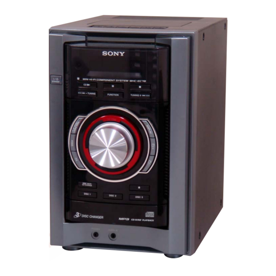
Photo : HCD-EC78
CD
Section
Tape deck
Section
(EXCEPT EC68: UK)
SPECIFICATIONS
Power output (rated):
50 W + 50 W (at 6 Ω, 1 kHz, 1% THD)
RMS output power (reference):
70 W + 70 W (per channel at 6 Ω, 1 kHz, 10% THD)
Inputs
AUDIO IN (stereo mini jack): Sensitivity 800 mV, impedance
22 kilohms
Outputs
PHONES (stereo mini jack): Accepts headphones with an
impedance of 8 Ω or more
SPEAKER: impedance
HCD-EC78: 8 Ω
HCD-EC68: 6 Ω
CD player section
System: Compact disc and digital audio system
λ
Laser: Semiconductor laser (
=770 – 810 nm)
Emission duration: continuous
Frequency response: 20 Hz – 20 kHz
Signal-to-noise ratio: More than 90 dB
Dynamic range: More than 88 dB
Tape deck section (except for the UK model)
Recording system: 4-track 2-channel, stereo
Model Name Using Similar Mechanism
Mechanism Type
Optical Pick-up Block Name
Model Name Using Similar Mechanism
Tape Transport Mechanism Type
Tuner section
FM stereo, FM/AM superheterodyne tuner
Antenna:
FM lead antenna
AM loop antenna
FM tuner section:
Tuning range:
87.5 – 108.0 MHz (50 kHz step)
Intermediate frequency: 10.7 MHz
AM tuner section:
Tuning range
Australian, Pan-American models:
530 – 1,710 kHz (with 10 kHz tuning interval)
531 – 1,710 kHz (with 9 kHz tuning interval)
European and Russian models:
531 – 1,602 kHz (with 9 kHz tuning interval)
Other models:
530 – 1,610 kHz (with 10 kHz tuning interval)
531 – 1,602 kHz (with 9 kHz tuning interval)
Intermediate frequency: 450 kHz
EXCEPT HCD-EC68: UK MODEL
COMPACT DISC DECK RECEIVER
COMPACT DISC RECEIVER
AEP Model
E Model
HCD-EC68/EC78
UK Model
Australian Model
HCD-EC68
NEW
CDM88A-K6BD90-WOD
KSM-213DCP
HCD-EC77
TCM-J1 or
CS-21SC-900TP
– Continued on next page –
HCD-EC68: UK MODEL
Advertisement
Table of Contents

Related Manuals for Sony HCD-EC68


Summary of Contents for Sony HCD-EC68
-
Page 1: Specifications
Ver. 1.0 2008.02 HCD-EC68/EC78 UK Model Australian Model HCD-EC68 • HCD-EC68 is the amplifi er, CD player, tape deck (except UK model) and tuner section in MHC-EC68. • HCD-EC78 is the amplifi er, CD player, tape deck and tuner section in MHC-EC78. -
Page 2: Table Of Contents
COMPONENTS IDENTIFIED BY MARK 0 OR DOTTED LINE WITH MARK 0 ON THE SCHEMATIC DIAGRAMS AND IN THE PARTS LIST ARE CRITICAL TO SAFE OPERATION. REPLACE THESE COMPONENTS WITH SONY PARTS WHOSE PART NUMBERS APPEAR AS SHOWN IN THIS MANUAL OR IN SUPPLEMENTS PUBLISHED BY SONY. - Page 3 HCD-EC68/EC78 SECTION 1 SERVICING NOTES MODEL IDENTIFICATION NOTES ON HANDLING THE OPTICAL PICK-UP – Back Panel – BLOCK OR BASE UNIT The laser diode in the optical pick-up block may suffer electrostat- ic break-down because of the potential difference generated by the charged electrostatic load, etc.
- Page 4 HCD-EC68/EC78 HOW TO OPEN THE TRAY WHEN POWER SWITCH TURN OFF lever door (CD) pull the tray by the hand. gear Turn a gear by a driver till a lever falls down to the position of the figure. HOW TO REMOVE THE KNOB (VOL)
- Page 5 HCD-EC68/EC78 CAPACITOR DISCHARGE FOR ELECTRIC SHOCK PREVENTION In checking the MAIN board, make a capacitor discharge of C622, C676, C677 and C678 for electric shock prevention. 800 Ω/2W C626 (EC68/EC78: E2, E3, E51, MX, AR), MAIN board C678 (EC78: AEP, RU)
-
Page 6: Basic Operations
HCD-EC68/EC78 SECTION 2 This section is extracted GENERAL from instruction manual. Compatibility with all MP3 encoding/writing software, recording Basic Operations Selecting a music source Using optional audio components device, and recording media cannot be guaranteed. Incompatible MP3 discs may produce noise or interrupted audio or may not play at all. -
Page 7: Other Operations
HCD-EC68/EC78 Other Operations Recording onto a tape (Except for the UK model) Use a TYPE I (normal) tape only. Creating your own CD program You can record just the portions you like from a sound (Program Play) source, including connected audio components. -
Page 8: Disassembly
HCD-EC68/EC78 SECTION 3 DISASSEMBLY • This set can be disassembled in the order shown below. 3-1. DISASSEMBLY FLOW 3-2. SIDE PANEL (L)/(R) (Page 9) 3-3. TOP PANEL (EC68: UK MODEL)/TOP PANEL BLOCK (EXCEPT EC68: UK MODEL) (Page 9) 3-4. TAPE MECHANISM DECK 3-5. -
Page 9: Side Panel (L)/(R)
HCD-EC68/EC78 Note: Follow the disassembly procedure in the numerical order shown below. 3-2. SIDE PANEL (L)/(R) two screws (BVTP3 × 10) two screws (BVTP3 × 10) four screws (case3 TP) side panel (L) side panel (R) four screws (case3 TP) 3-3. -
Page 10: Tape Mechanism Deck (Except Ec68: Uk Model)
HCD-EC68/EC78 3-4. TAPE MECHANISM DECK (EXCEPT EC68: UK MODEL) Note: This illustration is seeing top panel block from inside. two screws (2.6 × 8) DECK board bracket (deck) two screws (2.6 × 8) two screws (BVTP3 × 6) connector (CN501) -
Page 11: Front Panel Section
HCD-EC68/EC78 3-6. FRONT PANEL SECTION flexible flat cable (9 core) (CN605) flexible flat cable (27 core) (CN607) flexible flat cable (13 core) front panel section (CN302) lever pull the tray by hand. gear Turn a gear by a driver two screws till a lever falls down (BVTP3 ×... -
Page 12: Cd Mechanism Block
HCD-EC68/EC78 3-8. CD MECHANISM BLOCK flexible flat cable (21 core) (MAIN board: CN608/ CD board: CN201) CD mechanism block four screws (BVTP3 × 10) two tapes Note: When installing the CD mechanism section, flexible flat cable (13 core) install two tapes for prevention of noise. -
Page 13: Op Base Assy (Ksm-213D)
HCD-EC68/EC78 3-10. OP BASE ASSY (KSM-213D) op base assy (KSM-213D) flexible flat cable (16 core) (CN301) CD board Remove four solders. -
Page 14: Test Mode
HCD-EC68/EC78 SECTION 4 TEST MODE COLD RESET CD TRAY LOCK The cold reset clears all data including preset data stored in the This mode is for the antitheft of CD disc in shop. (not for trans- memory to initial conditions. Execute this mode when returning port) the set to the customer. - Page 15 HCD-EC68/EC78 [CD SERVO TEST MODE] CD Servo Test Mode Tree: Higher layer Lower layer of menu hierarchy This mode can check the servo system operations of the optical S Curve Mode LD ON pick-up system (= optical unit + CD board).
- Page 16 HCD-EC68/EC78 CD SERVICE MODE Contents of “CDM Errors” Error display example This mode can move the SLED of the optical pick-up, and also can M 0 FF 11 42 turn the optical pick-up laser power on and off. Procedure: 1 2 3 4 1.
- Page 17 HCD-EC68/EC78 Key Operation: 3 It indicates the on-going processing of optical pick-up system [DISPLAY]: (= optical unit + BD board) when the trouble has occurred. The display changes in the following order when- 01: The CD SHIP mode processing is in progress.
-
Page 18: Mechanical Adjustments
HCD-EC68/EC78 SECTION 5 SECTION 6 MECHANICAL ADJUSTMENTS ELECTRICAL ADJUSTMENTS PRECAUTION DECK SECTION 0 dB = 0.775V (EXCEPT EC68: UK model) 1. Clean the following parts with a denatured-alcohol-moistened 1. Demagnetize the record/playback head with a head demagne- swab : tizer. - Page 19 HCD-EC68/EC78 CD SECTION Adjustment Location: Record/Playback/Erase Head Note: 1. CD Block is basically constructed to operate without adjustment. 2. Use YEDS-18 disc (3-702-101-01) unless otherwise indicated. 3. Use an oscilloscope with more than 10 MΩ impedance. 4. Clean the object lens by an applicator with neutral detergent when the signal level is low than specifi...
- Page 20 HCD-EC68/EC78 0 dB = 1 μV TUNER SECTION AM FREQUENCY COVERAGE ADJUSTMENT (EC68: Mexican, Argentina, Australian/ [AM] EC78: Mexican, Argentina models) Reading on Digital Setting: Adjustment Part Frequency Display Voltmeter FUNCTION: AM L801 530 kHz 1.5 ± 0.1 V 60 cm Confi...
- Page 21 HCD-EC68/EC78 [FM Auto Stop Check] Adjustment Location and Connecting Points: – MAIN Board (Component Side) – generator 75 Ω L801 FM Frequency L804 Coverage Adjustment AM Tracking Adjustment L802 FM Detector Procedure : Adjustment 1. Turn the power on. 2. Input the following signal from Signal Generator to FM an- L803 tenna input directly.
- Page 22 HCD-EC68/EC78 MEMO...
-
Page 23: Diagrams
HCD-EC68/EC78 SECTION 7 DIAGRAMS THIS NOTE IS COMMON FOR PRINTED WIRING BOARDS AND SCHEMATIC DIAGRAMS. • Circuit Boards Location (In addition to this, the necessary note is printed in each block.) MAIN board For Printed Wiring Boards. For Schematic Diagrams. -
Page 24: Printed Wiring Board - Cd Board
HCD-EC68/EC78 7-1. PRINTED WIRING BOARD - CD Board - • See page 23 for Circuit Boards Location. • : Uses unleaded solder. CD BOARD (CONDUCTOR SIDE) CD BOARD (COMPONENT SIDE) M401 (SPINDLE) S201 (LIMIT) C404 C403 R402 IC401 TP124 M402... -
Page 25: Schematic Diagram - Cd Board
HCD-EC68/EC78 7-2. SCHEMATIC DIAGRAM - CD Board - • See page 37 for waveforms. • See page 38 for IC Block Diagrams. • See page 40 for IC Pin Function Description. (BX5BT/CBX1) R127 R126 C107 C136 R125 R120 R142 R139... -
Page 26: Printed Wiring Board - Deck Board (Except Ec68: Uk Model)
HCD-EC68/EC78 7-3. PRINTED WIRING BOARD - DECK Board (Except EC68: UK model) - 7-4. SCHEMATIC DIAGRAM - DECK Board (Except EC68: UK model) - • See page 37 for waveforms. • See page 23 for Circuit Boards Location. • : Uses unleaded solder. -
Page 27: Printed Wiring Board - Main Board
HCD-EC68/EC78 7-5. PRINTED WIRING BOARD - MAIN Board - • See page 23 for Circuit Boards Location. • : Uses unleaded solder. • Semiconductor Location Ref. No. Location (EC78) (EC78) HI AMP HI AMP (Page 31) M601 LOW AMP BOARD... -
Page 28: Schematic Diagram - Main Board (1/2)
HCD-EC68/EC78 7-6. SCHEMATIC DIAGRAM - MAIN Board (1/2) - MAIN BOARD (1/2) PROTECT CN601 Q601 R726 R725 R724 R672 KTA1266GR-AT TP601 16.6 JW750 JW751 JW752 VDD+ M601 TP602 D614 (FAN) Q603 R626 MA2J1110GLS0 R604 2SC3052F-T1-LF VDD+ 100k PROTECT 16.7 Q601, 602 10.8... -
Page 29: Schematic Diagram - Main Board (2/2)
HCD-EC68/EC78 7-7. SCHEMATIC DIAGRAM - MAIN Board (2/2) - • See page 37 for waveforms. • See page 38 for IC Block Diagrams. L801 MAIN BOARD (2/2) AM FREQUENCY COVERAGE D801 C819 SVC347A-TL-E 470p L805 R837 C820 C834 AM TRACKING... -
Page 30: Printed Wiring Board - Hi Amp Board (Ec78)
HCD-EC68/EC78 7-8. PRINTED WIRING BOARD - HI AMP Board (EC78) - • See page 23 for Circuit Boards Location. • : Uses unleaded solder. HI AMP BOARD JW157 JW151 R164 JW154 C160 C159 R163 C157 D152 R162 C170 Q152 C169... -
Page 31: Printed Wiring Board - Low Amp Board
HCD-EC68/EC78 7-10. PRINTED WIRING BOARD - LOW AMP Board - • See page 23 for Circuit Boards Location. • : Uses unleaded solder. LOW AMP BOARD CN102 D103 JW132 JW131 JW133 C109 R113 C110 C108 C107 C120 Q102 R111 R112... -
Page 32: Printed Wiring Board - Panel Board (Suffi X-12)
HCD-EC68/EC78 7-12. PRINTED WIRING BOARD - PANEL Board (Suffi x-12) - 7-13. PRINTED WIRING BOARD - PANEL Board (Suffi x-13) - • See page 23 for Circuit Boards Location. • See page 23 for Circuit Boards Location. • : Uses unleaded solder. -
Page 33: Schematic Diagram - Panel Board
HCD-EC68/EC78 7-14. SCHEMATIC DIAGRAM - PANEL Board - • See page 37 for waveforms. • See page 40 for IC Pin Function Description. LCD301 PANEL BOARD LIQUID CRYSTAL DISPLAY CN304 TP301 R301 O-TU-CE O-TU-CE TP302 R302 100 O-TU-DI O-TU-DI TP303... -
Page 34: Printed Wiring Boards - Key Section
HCD-EC68/EC78 7-15. PRINTED WIRING BOARDS - KEY Section - 7-16. SCHEMATIC DIAGRAM - KEY Section - • See page 23 for Circuit Boards Location. • : Uses unleaded solder. (SUFFIX-12) (SUFFIX-13) KEY CD BOARD PANEL PANEL BOARD BOARD KEY CD BOARD... -
Page 35: Printed Wiring Board - Pt Board
HCD-EC68/EC78 7-17. PRINTED WIRING BOARD - PT Board - • See page 23 for Circuit Boards Location. • : Uses unleaded solder. PT BOARD (EC68:E2,E3,E51/EC78:E2,E3,E51) S001 VOLTAGE SELECTOR 230-240V 220V 120V –2 –1 JW006 JW003 JW009 (EC68:AUS) EC68:E2,E3,E51,AR,AUS/ EC78:E2,E3,E51,AR EC68:MX/... -
Page 36: Schematic Diagram - Pt Board
HCD-EC68/EC78 7-18. SCHEMATIC DIAGRAM - PT Board - PT BOARD C051 PT001 EC68: AEP, UK, RU/ SUB POWER TRANSFORMER EC78: AEP, RU RY001 RY002 PT002 EC68: E2, E3, E51, MX, AR, AUS/ EC68: AEP, UK, RU/ EC68: E2, E3, E51, MX, AR, AUS/... - Page 37 HCD-EC68/EC78 • Waveforms – CD Board – – DECK Board – – PANEL Board – IC101 (RFi) CN501 (EH) IC301 (X1A) (CD play mode) 56 Vp-p 3 Vp-p 0.5 to 1.3 Vp-p 14 μs 30.5 μs 20 V/DIV, 5 μs/DIV 1 V/DIV, 10 μs/DIV...
-
Page 38: Ic Block Diagrams
HCD-EC68/EC78 • IC Block Diagrams – CD Board – IC401 BA5826SFP-E2 IC201 TK63115SCL-G@GT VIN 1 VO1(–) D.BUFF THERMAL & VO4(–) OVER CURRENT VO1(+) D.BUFF LEVEL D.BUFF PROTECTION SHIFT VO4(+) D.BUFF – VOLTAGE LEVEL GND 2 REFERENCE SHIFT VOUT ON/OFF RESET... - Page 39 HCD-EC68/EC78 IC801 LV23003VA 36 FM RF-IN AM RF-IN 35 GND2 34 FMRF-OUT 33 VCC2 FM-MIX 32 FM-OSC GND1 AM-MIX 31 AM-OSC VCC1 30 BO2 29 BO1 BUFFER LOW-PASS 28 LP-OUT FILTER 27 LP-IN 26 PD 25 AGC AMIF-IN 24 AMDET-OUT...
- Page 40 HCD-EC68/EC78 • IC Pin Function Description CD BOARD IC101 TC94A70FG-006 (D, HZ (CD-MP3 PROCESSOR) Pin No. Pin Name Description AVSS3 Ground terminal RFZi RF ripple zero crossing signal input terminal RFRP RF ripple signal output terminal SBAD/RFDC Sub beam addition signal or RF peak detection signal output terminal...
- Page 41 HCD-EC68/EC78 Pin No. Pin Name Description DOUT (PO6) Digital audio data output terminal Not used AOUT (PO7) Audio data output terminal Not used BCK (PO8) Bit clock signal output terminal Not used LRCK (PO9) L/R sampling clock signal output terminal...
- Page 42 HCD-EC68/EC78 PANEL BOARD IC301 MB90803PF-G-135E1 (SYSTEM CONTROLLER) Pin No. Pin Name Description SEG32 Segment drive signal output to the liquid crystal display O-AMP-ON Relay drive signal output terminal (for speaker) O-POWER Main power on/off control signal output terminal "H": on...
- Page 43 HCD-EC68/EC78 Pin No. Pin Name Description O-TU-DI Serial data output to the FM/AM DET Terminal for doubler circuit capacitor connection to develop liquid crystal display drive volt- VLCD COM0, COM1, CMO2, 59 to 62 Common drive signal output to the liquid crystal display...
-
Page 44: Exploded Views
HCD-EC68/EC78 SECTION 8 EXPLODED VIEWS Note: • -XX and -X mean standardized parts, so • Color Indication of Appearance Parts Ex- : 240V AC area in E model they may have some difference from the ample: : Chilean and Peruvian models original one. -
Page 45: Tape Deck Section (Except Ec68: Uk)
HCD-EC68/EC78 8-2. TAPE DECK SECTION (EXCEPT EC68: UK) not supplied supplied not supplied not supplied (DECK board) not supplied Note: When you exchange Ref.No.60, 62 or 63, Please refer to “HOW TO DISTINGUISH TAPE MECHANISM DECK (EXCEPT EC68: UK MODEL)” of the service note (5 page). -
Page 46: Front Panel Section
HCD-EC68/EC78 8-3. FRONT PANEL SECTION not supplied (KEY POWER board) not supplied supplied not supplied not supplied (KEY CD board) not supplied (JACK HOLD board) not supplied (JACK board) Ref. No. Part No. Description Remark Ref. No. Part No. Description... -
Page 47: Chassis Section
HCD-EC68/EC78 8-4. CHASSIS SECTION (EC78) main section not supplied M601 not supplied (AC HOLD board) not supplied CD mechanism section not supplied Ref. No. Part No. Description Remark Ref. No. Part No. Description Remark 1-832-838-21 CABLE, FLEXIBLE FLAT (13 CORE) -
Page 48: Main Section
HCD-EC68/EC78 8-5. MAIN SECTION (EC78) not supplied not supplied not supplied (HI AMP board) not supplied (REG board) not supplied not supplied not supplied not supplied (LOW AMP board) PT003: EC68/ PT004: EC78 not supplied not supplied (PT board) not supplied... -
Page 49: Cd Mechanism Section (Cdm88A-K6Bd90-Wod)
HCD-EC68/EC78 8-6. CD MECHANISM SECTION (CDM88A-K6BD90-WOD) not supplied (including sled motor (M402), spindle motor (M401)) not supplied sled motor (M402) spindle motor (M401) S201 Ref. No. Part No. Description Remark Ref. No. Part No. Description Remark 1-797-193-12 MECHANICAL, CD (DLM3A) -
Page 50: Electrical Parts List
HCD-EC68/EC78 SECTION 9 ELECTRICAL PARTS LIST Note: • Due to standardization, replacements in • RESISTORS : Mexican model the parts list may be different from the All resistors are in ohms. : Russian model parts specifi ed in the diagrams or the com- METAL: Metal-fi... - Page 51 HCD-EC68/EC78 DECK Ref. No. Part No. Description Remark Ref. No. Part No. Description Remark R113 1-216-833-11 METAL CHIP 1/10W < VIBRATOR > R114 1-216-833-11 METAL CHIP 1/10W X102 1-795-101-21 VIBRATOR, CERAMIC (16.9344MHz) R118 1-216-845-11 METAL CHIP 100K 1/10W ************************************************************ R120...
- Page 52 HCD-EC68/EC78 DECK HI AMP Ref. No. Part No. Description Remark Ref. No. Part No. Description Remark < SWITCH > < JUMPER RESISTOR > S501 1-762-369-11 SWITCH, SLIDE (REC/PB) JR501 1-216-864-11 SHORT CHIP ************************************************************ JR502 1-216-864-11 SHORT CHIP JR503 1-216-864-11 SHORT CHIP...
- Page 53 HCD-EC68/EC78 HI AMP JACK KEY CD KEY POWER LOW AMP Ref. No. Part No. Description Remark Ref. No. Part No. Description Remark R156 1-216-841-11 METAL CHIP 1/10W KEY POWER BOARD R159 1-216-821-11 METAL CHIP 1/10W ***************** R160 1-216-821-11 METAL CHIP...
- Page 54 HCD-EC68/EC78 LOW AMP MAIN Ref. No. Part No. Description Remark Ref. No. Part No. Description Remark R102 1-216-864-11 SHORT CHIP R103 1-216-824-11 METAL CHIP 1.8K 1/10W C606 1-162-968-11 CERAMIC CHIP 0.0047uF (EC78) (EC78) R103 1-216-827-11 METAL CHIP 3.3K 1/10W C607 1-100-566-91 CERAMIC CHIP 0.1uF...
- Page 55 HCD-EC68/EC78 MAIN Ref. No. Part No. Description Remark Ref. No. Part No. Description Remark C660 1-162-915-11 CERAMIC CHIP 10PF 0.5PF C822 1-126-965-91 ELECT 22uF C661 1-126-964-11 ELECT 10uF C823 1-126-923-91 ELECT 220uF C662 1-115-416-11 CERAMIC CHIP 0.001uF C824 1-165-908-11 CERAMIC CHIP 1uF...
- Page 56 HCD-EC68/EC78 MAIN Ref. No. Part No. Description Remark Ref. No. Part No. Description Remark D619 8-719-063-79 DIODE 1N4002B < TRANSISTOR > D620 8-719-063-79 DIODE 1N4002B D621 6-501-722-01 DIODE MAZ8043GMLS0 Q601 8-729-037-03 TRANSISTOR KTA1266GR-AT D622 6-501-752-01 DIODE MAZ8082GMLS0 Q602 8-729-120-28 TRANSISTOR...
- Page 57 HCD-EC68/EC78 MAIN Ref. No. Part No. Description Remark Ref. No. Part No. Description Remark R629 1-216-829-11 METAL CHIP 4.7K 1/10W R684 1-216-837-11 METAL CHIP 1/10W R630 1-216-841-11 METAL CHIP 1/10W R685 1-216-829-11 METAL CHIP 4.7K 1/10W R631 1-216-797-11 METAL CHIP...
- Page 58 HCD-EC68/EC78 MAIN PANEL Ref. No. Part No. Description Remark Ref. No. Part No. Description Remark R813 1-216-853-11 METAL CHIP 470K 1/10W A-1379-679-A PANEL BOARD, COMPLETE (EC78: AEP) R814 1-216-837-11 METAL CHIP 1/10W A-1379-692-A PANEL BOARD, COMPLETE (EC78: RU) R815 1-216-833-11...
- Page 59 HCD-EC68/EC78 PANEL Ref. No. Part No. Description Remark Ref. No. Part No. Description Remark D302 6-501-817-01 DIODE MA2J1110GLS0 R307 1-216-809-11 METAL CHIP 1/10W D303 6-500-334-01 DIODE MC2836-T112-1 R308 1-216-809-11 METAL CHIP 1/10W D304 6-501-817-01 DIODE MA2J1110GLS0 R309 1-216-809-11 METAL CHIP...
- Page 60 HCD-EC68/EC78 PANEL Ref. No. Part No. Description Remark Ref. No. Part No. Description Remark R368 1-216-833-11 METAL CHIP 1/10W R369 1-216-821-11 METAL CHIP 1/10W < ROTARY ENCODER > R370 1-216-821-11 METAL CHIP 1/10W R371 1-216-821-11 METAL CHIP 1/10W S301 1-786-417-11...
- Page 61 HCD-EC68/EC78 Ref. No. Part No. Description Remark Ref. No. Part No. Description Remark REG BOARD ********* < CAPACITOR > C698 1-100-566-91 CERAMIC CHIP 0.1uF < IC > IC601 8-759-231-56 IC TA7809S < CABLE HOLDER > W610 1-824-027-21 HOLDER, CABLE 3P...
-
Page 62: Revision History
HCD-EC68/EC78 REVISION HISTORY Checking the version allows you to jump to the revised page. Also, clicking the version at the top of the revised page allows you to jump to the next revised page. Ver. Date Description of Revision 2008.02...
Need help?
Do you have a question about the HCD-EC68 and is the answer not in the manual?
Questions and answers