Table of Contents
Advertisement
SERVICE MANUAL
Ver 1.2 2001.12
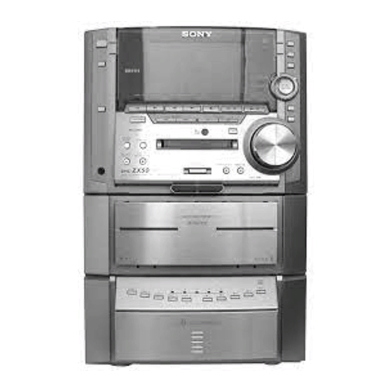
HCD-ZX50MD is the tuner, deck, CD, MD and
amplifier section in DHC-ZX50MD.
Amplifier section
AUDIO POWER SPECIFICATIONS:
(US model only)
POWER OUTPUT AND TOTAL HARMONIC
DISTORTION:
with 8 ohm loads both channels driven, from 120–
10,000 Hz; rates 80 watts per channel minimum
RMS power, with no more than 10 % total
harmonic distortion from
250 milliwatts to rated output.
Total harmonics distortion Less than 0.07 %
(8 ohms at 1 kHz, 50 W)
European model:
DIN power output (rated) 60 + 60 watts
(8 ohms at 1 kHz, DIN)
Continuous RMS power output (reference)
80 + 80 watts
(8 ohms at 1 kHz,
10 % THD)
Music power output (reference)
140 + 140 watts
(8 ohms at 1 kHz,
10 % THD)
Sony Corporation
9-929-512-13
2001L0200-1
Home Audio Company
© 2001.12
Published by Sony Engineering Corporation
HCD-ZX50MD
Model Name Using Similar Mechanism
CD Mechanism Type
CD
SECTION
Base Unit Type
Optical Pick-up Type
Model Name Using Similar Mechanism
MD
MD Mechanism Type
SECTION
Optical Pick-up Type
Model Name Using Similar Mechanism
TAPE DECK
SECTION
Tape Transport Mechanism Type
SPECIFICATIONS
Other models:
The following measured at 120/220/240 V AC, 50/60 Hz
DIN power output (rated) 115 + 115 watts
(6 ohms at 1 kHz, DIN)
Continuous RMS power output (reference)
150 + 150 watts
(6 ohms at 1 kHz,
10 % THD)
Inputs
VIDEO (AUDIO) IN:
voltage 250 mV,
(phono jacks)
impedance 47 kilohms
MIC:
sensitivity 1 mV,
(mini jack)
impedance 10 kilohms
(Asian model only)
Outputs
PHONES:
accepts headphones of
(stereo mini jack)
8 ohms or more
FRONT SPEAKER:
US and European models: accepts impedance of 8 to 16 ohms
Other models:
accepts impedance of 6 to 16 ohms
SUPER WOOFER:
Voltage 1 V, impedance 1 kilohms
MINI Hi-Fi COMPONENT SYSTEM
US Model
AEP Model
UK Model
E Model
Australian Model
NEW
CDM53F-K4BD40
BU-K4BD40
KSM-213DHAP/Z-NP
MDS-JE640
MDM-7B
KMS-260B/J1N
HCD-ZX10
TCM-230AWR12
CD player section
System
Compact disc and digital audio
system
Laser
Semiconductor laser
(λ=780nm)
Emission duration: continuous
Max. 44.6 µW*
Laser output
*This output is the value measured
at a distance of 200 mm from the
objective lens surface on the
Optical Pick-up Block with 7 mm
aperture.
Wavelength
780 – 790 nm
Frequency response
2 Hz – 20 kHz (±0.5 dB)
Signal-to-noise ratio
More than 90 dB
Dynamic range
More than 90 dB
— Continued on next page —
1
Advertisement
Table of Contents

Related Manuals for Sony HCD-ZX50MD


Summary of Contents for Sony HCD-ZX50MD
- Page 1 SERVICE MANUAL US Model AEP Model Ver 1.2 2001.12 UK Model E Model Australian Model HCD-ZX50MD is the tuner, deck, CD, MD and amplifier section in DHC-ZX50MD. Model Name Using Similar Mechanism CD Mechanism Type CDM53F-K4BD40 SECTION Base Unit Type...
- Page 2 Recording system 4-track 2-channel stereo Frequency response 40 – 13,000 Hz (±3 db), Mass (DOLBY NR OFF) using Sony TYPE I cassette US model: Approx. 11.5 kg 40 – 14,000 Hz (±3 db), European model: Approx. 11.5 kg using Sony TYPE II cassette Other models: Approx.
- Page 3 Change the MD with another one and start The component has internal problems. recording over from the beginning. p Consult your nearest Sony dealer. C13 / Read Error E0101 / LASER NG The MD cannot read the disc information There is a problem with the laser pickup.
- Page 4 ITEMS OF ERROR HISTORY MODE ITEMS AND CONTENTS Selecting the Test Mode Display History op rec tm Displays the total recording time. When the total recording time is more than 1 minute, displays the hour and minute When less than 1 minute, displays “Under 1 min” The display time is the time the laser is set to high power, which is about 1/4 of the actual recording time.
- Page 5 Table of Error Codes Error Code Description Could not load Loading switches combined incorrectly Timed out without reading the top of PTOC Could read top of PTOC, but detected error Timed out without accessing UTOC Timed out without reading UTOC Error in UTOC Could not start playback Error in sector...
-
Page 6: Table Of Contents
TABLE OF CONTENTS 1. SERVICING NOTES ..........7-12. Schematic Diagram – Main (2/4) Section – ..... 67 7-13. Schematic Diagram – Main (3/4) Section – ..... 68 7-14. Schematic Diagram – Main (4/4) Section – ..... 69 2. GENERAL ................ 15 7-15. - Page 7 Use of controls or adjustments or performance of procedures LIST ARE CRITICAL TO SAFE OPERATION. REPLACE THESE other than those specified herein may result in hazardous radiation COMPONENTS WITH SONY PARTS WHOSE PART NUMBERS exposure. APPEAR AS SHOWN IN THIS MANUAL OR IN SUPPLEMENTS PUBLISHED BY SONY.
- Page 8 Ver 1.2 2001.12 SERVICE POSITION Jig (J-2501-076-A) CN701 CN503 • CD MECHANISM BLOCK Jig (J-2501-165-A) Jig (J-2501-011-A) Jig (J-2501-167-A)
- Page 9 • BD (CD) BOARD To repair the BD (CD) board,remove the bottom plate. Bottom view...
- Page 10 JIG FOR CHECKING BD (MD) BOARD WAVEFORM The special jig (J-2501-196-A) is useful for checking the waveform of the BD (MD) board. The names of terminals and the checking items to be performed are shown as follows. GND : Ground I+3V : For measuring IOP (Check the deterioration of the optical pick-up laser) IOP : For measuring IOP (Check the deterioration of the optical pick-up laser) : TRK error signal (Traverse adjustment)
- Page 11 Iop DATA RECORDING AND DISPLAY WHEN OPTICAL PICK-UP AND NON-VOLATILE MEMORY (IC195 OF BD (MD) BOARD) ARE REPLACED The Iop value labeled on the optical pick-up can be recorded in the non-volatile memory. By recording the value, it will eliminate the need to look at the value on the label of the optical pick-up.
- Page 12 CHECKS PRIOR TO PARTS REPLACEMENT AND ADJUSTMENTS Before performing repairs, perform the following checks to determine the faulty locations up to a certain extent. Details of the procedures are described in “6 Electrical Adjustments”. • 6-6-2. Laser power check (see page 43) •...
- Page 13 RETRY CAUSE DISPLAY MODE • In this test mode, the causes for retry of the unit during recording can be displayed on the fluorescent indicator tube. During playback, the “track mode” for obtaining track information will be set. This is useful for locating the faulty part of the unit. •...
- Page 14 Reading the Track Mode Display Higher Bits Lower Bits Details Hexa- Hexadecimal decimal b7 b6 b5 b4 b3 b2 b1 b0 When 0 When 1 Binary Emphasis ON Emphasis OFF Stereo Monaural This is 2-bit display. Normally 01. 01:Normal audio. Others:Invalid Invalid Audio (Normal) Digital copy...
-
Page 15: General
SECTION 2 GENERAL 3 45 678 wj wk wl e; ?/1 button and indicator PHONES jack TAPE A h button and indicator FUNCTION button TAPE A H button and indicator DISPLAY button TAPE B h button and indicator TIMER SELECT indicator TAPE B H button and indicator . - Page 16 This section is extracted from instruction manual. Getting Started...
- Page 17 Additional Information...
-
Page 18: Disassembly
SECTION 3 DISASSEMBLY Note : Follow the disassembly procedure in the numerical order given. 1 three screws (BVTT 3 × 8) 3-1. CASE 5 Remove the case in the arrow direction. 4 three screws (case 3 TP2) 2 two screws (BVTT 3 ×... -
Page 19: Md Mechanism Section
3-3. MD MECHANISM SETION TAPE MECHANISM DECK SECTION (TCM-230AWR12) 4 two screws (BVTP 3 × 8) 5 MD mechanism deck section (MDM-7B) 2 two screws (BVTP 3 × 8) 1 three screws (BVTP 3 × 8) 3 tape mechanism deck section (TCM-230AWR12) 3-4. -
Page 20: Md Mechanism Deck Section (Mdm-7B)
3-5. MD MECHANISM DECK SECTION (MDM-7B) 1 three screws (BVTP 3 × 8) 2 plate (B), shield qs two screws (BVTPWH M3), step 5 flat type wire (17core) (CN1004) 6 flat type wire (27core) (CN1003) qd MD mechanism deck (MDM-7B) qa two screws (BVTPWH M3), step 3 screw... -
Page 21: Cd Base Unit (Bu-K4Bd40)
3-7. CD BASE UNIT (BU-K4BD40) 5 CD base unit (BU-K4BD40) 4 two springs (insulator), compression 4 two springs (insulator), compression 2 chassis 3 two screws (PTPWH M 2.6) 3 two screws (PTPWH M 2.6) 1 three screws (BVTP 3 × 6) 3-8. -
Page 22: Fitting Base (Guide) Assy, Bracket (Chassis) And Fitting Base (Magnet) Assy
3-9. FITTING BASE (GUIDE) ASSY, BRACKET (CHASSIS) AND FITTING BASE (MAGNET) ASSY 7 four screws (BVTP M2.6) 2 four screws (BVTP M2.6) 8 base (magnet) assy, fitting 4 five screws (BVTP M2.6) 6 connector (CN710) 5 bracket (chassis) 3 base (guide) assy, fitting 1 two connectors (CN709, 715) -
Page 23: Chassis (Mold B) Section, Stocker Section And Slider (Selection)
3-11. CHASSIS (MOLD B) SECTION, STOCKER SECTION AND SLIDER (SELECTION) Note : In mounting the parts, refer to page 24 and 25. 6 two screws (PTPWH M2.6) 5 stocker section 7 slider (selection) 8 washer 9 compression 1 three screws spring pulley (LD) (BVTP M2.6) -
Page 24: Slider (Selection) Installation
3-13. SLIDER (SELECTION) INSTALLATION 6 two screws (PTPWH M2.6) 2 gear (chuking) rotary encoder 5 washer 4 compression spring 7 Insert the slider (selection) into the portion A. Align with the slot of rotary encoder. portion A 3 convex portion of slider (selection) gear (chuking) 1 rotary encoder... -
Page 25: Chassis (Mold B) Section Installation
3-15. CHASSIS (MOLD B) SECTION INSTALLATION 3 three screws (BVTP M2.6) 2 Insert the gear (eject) 1 Insert the portion A of under the gear (LD chassis (mold B) section deceleration). portion A into the portion B of slider (selection). gear (LD deceleration) portion B of slider (selection) -
Page 26: Test Mode
SECTION 4 TEST MODE [MC Cold Reset] [Change-over of MW Tuner Step between 9 kHz and • The cold reset clears all data including preset data stored in the 10 kHz] RAM to initial conditions. Execute this mode when returning •... - Page 27 [MC Test Mode] • This mode is used to check operations of the respective sections of Amplifier, Tuner, CD and Tape. Procedure: Press the ?/1 button to turn on the set. Press the three buttons of x , DISPLAY and DISC 3 simultaneously.
- Page 28 [Aging Mode] This mode can be used for operation check of CD section and tape deck section. • If an error occurred: The aging operation stops and display status. • If no error occurs: The aging operation continues repeatedly. 1. Operating method of Aging Mode Turn on the main power and select “CD”...
- Page 29 2. Correction of Errors [When due to tape deck] Stopped while tape aging operation with the ”” displayed state. [When due to CD] Press x , DISPLAY , and CD Z together to display the error code. • Display of number of mechanism errors Move the stick to the left and right to display “CDM Err Count *”.
- Page 30 4-1. PRECAUTIONS FOR USE OF TEST MODE • As loading related operations will be performed regardless of the test mode operations being performed, be sure to check that the disc is stopped before setting and removing it. Even if the MD Z button is pressed while the disc is rotating during continuous playback, continuous recording, etc., the disc will not stop rotating.
- Page 31 4-5. SELECTING THE TEST MODE There are 26 types of test modes as shown below. The groups can be switched by moving the multi-stick. After selecting the group to be used, press the PUSH ENTER button. After setting a certain group, move the multi-stick to switche between these modes. Refer to “Group”...
- Page 32 4-5-1. Operating the Continuous Playback Mode 1. Entering the continuous playback mode 1 Set the disc in the unit. (Whichever recordable discs or discs for playback only are available.) 2 Move the multi-stick and display “CPLAY1MODE”(C34). 3 Press the PUSH ENTER button to change the display to “CPLAY1MID”. 4 When access completes, the display changes to “C = AD = ”.
- Page 33 4-6. FUNCTIONS OF OTHER BUTTONS Function REC IT Contents Sets continuous playback when pressed in the STOP state. When pressed during continuous PUSH ENTER playback, the tracking servo turns ON/OFF. CLEAR Stops continuous playback and continuous recording. J (FF) The sled moves to the outer circumference only when this is pressed. j (FR) The sled moves to the inner circumference only when this is pressed.
- Page 34 4-8. MEANINGS OF OTHER DISPLAYS Contents Display When Lit When Off Servo ON Servo OFF Tracking servo OFF Tracking servo ON MD REC Recording mode ON Recording mode OFF TRACK CLV low speed mode CLV normal mode L.SYNC ABCD adjustment completed OVER Tracking offset cancel ON Tracking offset cancel OFF...
-
Page 35: Mechanical Adjustments
SECTION 5 SECTION 6 MECHANICAL ADJUSTMENTS ELECTRICAL ADJUSTMENTS Precaution DECK SECTION 0 dB=0.775V 1. Clean the following parts with a denatured alcohol-moistened swab: 1. Demagnetize the record/playback head with a head demagnetizer. record/playback heads pinch rollers 2. Do not use a magnetized screwdriver for the adjustments. erase head rubber belts 3. - Page 36 3. Mode: Playback 6. Adjust RV1002 of the LEAF SW board so that the reading of the frequency counter becomes 3000 ± 90 Hz. test tape 7. Press the "/1 button, after the turned ON. P-4-A100 main board CN301 (10kHz, –10dB) 8.
- Page 37 Record Bias Adjustment (Deck B) Record Level Adjustment (Deck B) Procedure: Procedure: INTRODUCTION INTRODUCTION When set to the test mode performed in Tape Speed Adjust- When set to the test mode performed in Tape Speed Adjust- ment, when the tape is rewound after recording, the “REC memory ment, when the tape is rewound after recording, the “REC memory mode”...
- Page 38 Note: Clear RF signal waveform means that the shape “◊” can be CD SECTION clearly distinguished at the center of the waveform. Note : RF signal waveform 1. CD Block is basically designed to operate without adjustment. Therefore, check each item in order given. VOLT/DIV : 200mV 2.
- Page 39 Adjustment Location : [ BD (CD) BOARD ] — SIDE B — (RF) IC102 (VC) (AGCCON) (FEO) (XPCK) (TEO) (GND)
- Page 40 MD SECTION 6-1. PARTS REPLACEMENT AND ADJUSTMENT If malfunctions caused by Optical pick-up such as sound skipping are suspected, follow the following check. Check before replacement Start 6-6-2. Laser Power Check (See page 43) 6-6-3. Iop Compare (See page 43) 6-6-4.
- Page 41 Adjustment flow • Abbreviation Start OP: Optical pick-up After turning off and then on the power, initialize the EEPROM Replace IC195 For details, refer to 4-11. WHEN MEMORY NG IS DISPLAYED (See page 34) 6-7. INITIAL SETTING OF ADJUSTMENT VALUE Replace OP or IC195 (See page 46) 6-9.
-
Page 42: Servicing Notes
6-2. PRECAUTIONS FOR CHECKING LASER DIODE EMISSION To check the emission of the laser diode during adjustments, never view directly from the top as this may lose your eye-sight. 6-3. PRECAUTIONS FOR USE OF OPTICAL PICK- UP (KMS-260B) As the laser diode in the optical pick-up is easily damaged by static electricity, solder the laser tap of the flexible board when using it. - Page 43 6-5. USING THE CONTINUOUSLY RECORDED DISC Checking Procedure: 1. Set the laser power meter on the objective lens of the optical * This disc is used in focus bias adjustment and error rate check. pick-up. (If cannot set properly, press the m or M button The following describes how to create a continuous recording while REC IT is off and move the optical pick-up.) disc.
- Page 44 6-6-4. Auto Check 6. Observe the waveform of the oscilloscope, and check that the This test mode performs CREC and CPLAY automatically for specified value is satisfied. mainly checking the characteristics of the optical pick-up. To (Read power traverse checking) perform this test mode, the laser power must first be checked.
- Page 45 6-6-8. C PLAY Check 16. Observe the waveform of the oscilloscope, and check that the specified value is satisfied. Do not move the Multi stick. MO Error Rate Check (Traverse Waveform) Checking Procedure : 1. Load a continuously recorded test disc (MDW-74/GA-1). (Refer to “6-5.
- Page 46 Adjusting Procedure : 6-7. INITIAL SETTING OF ADJUSTMENT VALUE 1. Move the multi-stick and display “TEMP ADJUS” (C03). 2. Press the PUSH ENTER button and select the “TEMP ADJUS” Note: (C03) mode. Mode which sets the adjustment results recorded in the non-vola- 3.
- Page 47 7. Then, move the multi-stick and display “LDPWR CHECK” 6-12. TRAVERSE ADJUSTMENT (C13). Connection : 8. Press the PUSH ENTER button once and display “LD 0.9 mW Oscilloscope ”. Check that the reading of the laser power meter become 0.85 to 0.91 mW. BD (MD) board 9.
- Page 48 6-13. FOCUS BIAS ADJUSTMENT 11. Move the multi-stick until the waveform of the oscilloscope moves closer to the specified value. Adjusting Procedure : In this adjustment, waveform varies at intervals of approx. 2%. 1. Load a test disk (MDW-74/GA-1). Adjust the waveform so that the specified value is satisfied as 2.
- Page 49 6-14. ERROR RATE CHECK 6-16. AUTO GAIN CONTROL OUTPUT LEVEL 6-14-1. CD Error Rate Check ADJUSTMENT Checking Procedure : Be sure to perform this adjustment when the Optical pick-up is re- 1. Load a check disc (MD) TDYS-1. placed. 2. Move the multi-stick and display “CPLAY1MODE” (C34). If the adjustment results becomes “Adjust NG!”, the Optical pick- 3.
- Page 50 6-17. ADJUSTING POINTS AND CONNECTING POINTS [BD (MD) BOARD] (SIDE A) CN101 D101 [BD (MD) BOARD] (SIDE B) IC101 CN105 IC102 NOTE IC151 IC190 IC195 1 27 CN103 CN102 NOTE:It is useful to use the jig. for checking the waveform. (Refer to Servicing Note on page 10.)
-
Page 51: Diagrams
SECTION 7 DIAGRAMS 7-1. CIRCUIT BOARDS LOCATION TRANS board PANEL board MAIN board SUB PANEL board HP board LEAF SW board MIC board FRONT AMP board CD SW board AUDIO board SUB TRANS board (US,AEP,UK,G,AED,CIS model) CLAMP MOTOR board TUNER UNIT DIGITAL board BD (CD) board BD (MD) board... - Page 52 THIS NOTE IS COMMON FOR PRINTED WIRING • Indication of transistor BOARDS AND SCHEMATIC DIAGRAMS. (In addition to this, the necessary note is printed in each block.) These are omitted. For schematic diagrams. Note: • All capacitors are in µF unless otherwise noted. pF: µµF 50 WV or less are not indicated except for electrolytics and tantalums.
- Page 53 • WAVEFORMS – BD (MD) SECTION – – BD (CD) SECTION – – MAIN SECTION – – MD DIGITAL SECTION – – PANEL SECTION – IC101 ek (RF) IC101 t; IC401 qa IC1001 w; IC701 oa RFAC XOUT 1.3Vp-p 1.3Vp-p 2.7Vp-p 10.0MHz 4.4Vp-p...
-
Page 54: Block Diagrams
HCD-ZX50MD 7-2. BLOCK DIAGRAMS – CD SECTION – OPTICAL PICK-UP BLOCK (KSM-213DHAP/Z-NP) IC101 DIGITAL SERVO D+5V DETECTOR IC103 DIGITAL SIGNAL PRCESSOR RF AMP DIGITAL D OUT ERROR CORRECTOR IC551 PCMD RF AC 2,12,13 RF EQ SECTION SUMMING REGISTER OPTICAL DEMODULATOR... -
Page 55: Md Section
HCD-ZX50MD – MD SECTION – IC151 (1/2) OVER WRITE EFMO ADDT HEAD DRIVE IC181, Q181, 182 DATA1 FILI SAMPLING DATAI HR901 SCTX RATE OVER WRITE HEAD XBCKI XBCK1 CONVERTER DIGITAL SIGNAL PROCESSOR, LRCKI CLTV LRCK1 EFM/ACIRC ENCODER/DECODER, SHOCK PROOF MEMORY CONTROLLER,... -
Page 56: Syscon/Servo Section
HCD-ZX50MD – SYSCON/SERVO SECTION – IC401 (2/2) IC701 MASTER CONTROL SYSTEM CONTROL IC703 XC-IN FL DRIVER X401 32.768MHz D704, Q703 X IN Q701 XC-OUT X701 GRID EXT CLK DISC IN FL701 LEVEL 12.5MHz GRID EXT RESET RESET DET. DISC-SENS SHIFT... -
Page 57: Main Section
HCD-ZX50MD – MAIN SECTION – IC801 POWER AMP US,AEP,UK,G,AED,CIS • RCH is omitted LOUT IC101 – • SHIGNAL PATH SOUND PROCESSOR SECTION : CD (Page 55) J102 REC B2 L IN WOOFER : FM SW OUT IC801 E,MX,AR,HK,MY,SP,KR,AUS Q130 POWER AMP... -
Page 58: Printed Wiring Board - Deck Section
HCD-ZX50MD 7-3. PRINTED WIRING BOARD – DECK SECTION – • See page 51 for Circuit Boards Location. JW15 There are few cases that the part isn’t mounted in model is printed on diagram. -
Page 59: Schematic Diagram - Deck Section
HCD-ZX50MD 7-4. SCHEMATIC DIAGRAM – DECK SECTION – (Page 66) Note: The components identified by mark 0 or dotted line with mark 0 are critical for safety. Replace only with part number specified. -
Page 60: Printed Wiring Board - Cd Section
HCD-ZX50MD 7-5. PRINTED WIRING BOARD – CD SECTION – • See page 51 for Circuit Boards Location. • Semiconductor • Semiconductor Location Location Ref. No. Location Ref. No. Location IC101 Q101 IC102 Q102 IC103 There are few cases that the part isn’t mounted in... -
Page 61: Schematic Diagram - Cd Section
HCD-ZX50MD 7-6. SCHEMATIC DIAGRAM – CD SECTION – • See page 53 for Waveforms. • See page 91 for IC Block Diagrams. • See page 94 for IC Pin Functions. PIN FUNCTION... -
Page 62: Printed Wiring Board - Md Section
HCD-ZX50MD 7-7. PRINTED WIRING BOARD – MD SECTION – • See page 51 for Circuit Boards Location. • Semiconductor • Semiconductor Location Location Ref. No. Location Ref. No. Location Ref. No. Location D101 D181 IC181 D183 IC190 Q101 IC195 Q131... -
Page 63: Schematic Diagram - Md (1/2) Section
HCD-ZX50MD 7-8. SCHEMATIC DIAGRAM – MD (1/2) SECTION – • See page 53 for Waveforms. • See page 90 for IC Block Diagrams. • See page 96 for IC Pin FUnctions. FUNCTION... -
Page 64: Schematic Diagram - Md (2/2) Section
HCD-ZX50MD 7-9. SCHEMATIC DIAGRAM – MD (2/2) SECTION – • See page 53 for Waveforms. • See page 90 for IC Block Diagrams. • See page 97 for IC Pin FUnctions. • See page 62 for Printed WIring Board. PIN FUNCTION... -
Page 65: Printed Wiring Board - Main Section
HCD-ZX50MD • Semiconductor Location Ref. No. Location 7-10. PRINTED WIRING BOARD – MAIN SECTION – • See page 51 for Circuit Boards Location. D100 D101 D181 I-12 D182 H-11 D501 D502 D503 D504 D505 D506 D507 D508 D509 D511 D512... -
Page 66: Schematic Diagram - Main (1/4) Section
HCD-ZX50MD 7-11. SCHEMATIC DIAGRAM – MAIN (1/4) SECTION – • See page 65 for Printed WIring Board. -
Page 67: Schematic Diagram - Main (2/4) Section
HCD-ZX50MD 7-12. SCHEMATIC DIAGRAM – MAIN (2/4) SECTION – • See page 65 for Printed WIring Board. -
Page 68: Schematic Diagram - Main (3/4) Section
HCD-ZX50MD 7-13. SCHEMATIC DIAGRAM – MAIN (3/4) SECTION – • See page 53 for Waveforms. • See page 102 for IC Pin Functions. • See page 91 for IC Block Diagrams. • See page 65 for Printed WIring Board. PIN FUNCTION... -
Page 69: Schematic Diagram - Main (4/4) Section
HCD-ZX50MD 7-14. SCHEMATIC DIAGRAM – MAIN (4/4) SECTION – • See page 91 for IC Block Diagrams. • See page 65 for Printed Wiring Board. -
Page 70: Printed Wiring Board - Digital (Side A) Section
HCD-ZX50MD 7-15. PRINTED WIRING BOARD – DIGITAL (SIDE A) SECTION – • See page 51 for Circuit Boards Location. • Semiconductor Location Ref. No. Location IC1001 IC1002 IC1005 IC1006 Q1003 Q1004 There are few cases that the part isn’t mounted in... -
Page 71: Printed Wiring Board - Digital (Side B) Section
HCD-ZX50MD 7-16. PRINTED WIRING BOARD – DIGITAL (SIDE B) SECTION – • See page 51 for Circuit Boards Location. • Semiconductor Location Ref. No. Location IC1004 Q1001 Q1002 There are few cases that the part isn’t mounted in model is printed on diagram. -
Page 72: Schematic Diagram - Digital (1/2) Section
HCD-ZX50MD 7-17. SCHEMATIC DIAGRAM – DIGITAL (1/2) SECTION – • See page 53 for Waveforms. • See page 92 for IC Block Diagrams. • See page 100 for IC Pin Functions. • See page 70 for Printed Wiring Board. PIN FUNCTION... -
Page 73: Schematic Diagram - Digital (2/2) Section
HCD-ZX50MD 7-18. SCHEMATIC DIAGRAM – DIGITAL (2/2) SECTION – • See page 92 for IC Block Diagrams. • See page 70 for Printed Wiring Board. -
Page 74: Printed Wiring Board - Amp (Us, Aep, Uk, G, Aed, Cis Model) Section
HCD-ZX50MD 7-19. PRINTED WIRING BOARD – AMP (US, AEP, UK, G, AED, CIS model) SECTION – • See page 51 for Circuit Boards Location. • Semiconductor Location Ref. No. Location D801 D802 D821 D831 D851 D871 D881 D911 D963 D981... -
Page 75: Schematic Diagram - Amp (Us, Aep, Uk, G, Aed, Cis Model) Section
HCD-ZX50MD 7-20. SCHEMATIC DIAGRAM – AMP (US, AEP, UK, G, AED, CIS model) SECTION –... -
Page 76: Printed Wiring Board - Amp
HCD-ZX50MD 7-21. PRINTED WIRING BOARD – AMP (E, MX, AR, HK, MY, SP, KR, AUS model) SECTION – • See page 51 for Circuit Boards Location. • Semiconductor Location Ref. No. Location D801 D802 D821 D831 D851 D871 D881 D911... -
Page 77: Schematic Diagram - Amp (E, Mx, Ar, Hk, My, Sp, Kr, Aus Model) Section
HCD-ZX50MD 7-22. SCHEMATIC DIAGRAM – AMP (E, MX, AR, HK, MY, SP, KR, AUS model) SECTION –... -
Page 78: Printed Wiring Board - Panel Section
HCD-ZX50MD 7-23. PRINTED WIRING BOARD – PANEL SECTION – • See page 51 for Circuit Boards Location. • Semiconductor Location Ref. No. Location Ref. No. Location Ref. No. Location Ref. No. Location D601 D756 IC702 Q603 D602 D761 IC703 Q663... -
Page 79: Schematic Diagram - Panel Section
HCD-ZX50MD 7-24. SCHEMATIC DIAGRAM – PANEL SECTION – • See page 53 for Waveforms. • See page 93 for IC Block Diagrams. • See page 105 for IC Pin Functions. PIN FUNCTION... -
Page 80: Printed Wiring Board - Switch Section
HCD-ZX50MD 7-25. PRINTED WIRING BOARD – SWITCH SECTION – • See page 51 for Circuit Boards Location. • Semiconductor Location Ref. No. Location D605 D606 D609 D610 D611 D612 D613 D614 D617 D618 D619 D651 D652 Q605 Q607 Q609 Q611... -
Page 81: Schematic Diagram - Switch Section
HCD-ZX50MD 7-26. SCHEMATIC DIAGRAM – SWITCH SECTION –... -
Page 82: Printed Wiring Board - Cd Mechanism Section
HCD-ZX50MD 7-27. PRINTED WIRING BOARD – CD MECHANISM SECTION – • See page 51 for Circuit Boards Location. (Page 65) (Page 65) There are few cases that the part isn’t mounted in model is printed on diagram. -
Page 83: Schematic Diagram - Cd Mechanism Section
HCD-ZX50MD 7-28. SCHEMATIC DIAGRAM – CD MECHANISM SECTION – (Page 68) (Page 68) -
Page 84: Printed Wiring Board - Leaf Sw Section
HCD-ZX50MD 7-29. PRINTED WIRING BOARD – LEAF SW SECTION – • See page 51 for Circuit Boards Location. CAPSTAN MOTOR A DECK B DECK PLUNGER PLUNGER There are few cases that the part isn’t mounted in model is printed on diagram. -
Page 85: Printed Wiring Board - Mic Section
HCD-ZX50MD 7-31. PRINTED WIRING BOARD – MIC SECTION – • See page 51 for Circuit Boards Location. 7-32. SCHEMATIC DIAGRAM – MIC SECTION – There are few cases that the part isn’t mounted in model is printed on diagram. -
Page 86: Printed Wiring Board - Power Supply (Us, Aep, Uk, G, Aed, Cis Model) Section
HCD-ZX50MD 7-33. PRINTED WIRING BOARD – POWER SUPPLY (US, AEP, UK, G, AED, CIS model) SECTION – • See page 51 for Circuit Boards Location. US MODEL JW915 EXCEPT US EXCEPT US JW914 US MODEL • Semiconductor Location Ref. No. -
Page 87: Schematic Diagram - Power Supply (Us, Aep, Uk, G, Aed, Cis Model) Section
HCD-ZX50MD 7-34. SCHEMATIC DIAGRAM – POWER SUPPLY (US, AEP, UK, G, AED, CIS model) SECTION – T6.3AL T6.3AL 125V... -
Page 88: Printed Wiring Board - Power Supply
HCD-ZX50MD 7-35. PRINTED WIRING BOARD – POWER SUPPLY (E, MX, AR, HK, MY, SP, KR, AUS model) SECTION – • See page 51 for Circuit Boards Location. VOLTAGE SELECTOR E, AR, HK, MY, SP, KR E, AR, HK, MY, SP, AUS There are few cases that the part isn’t mounted in... -
Page 89: Schematic Diagram - Power Supply (E, Mx, Ar, Hk, My, Sp, Kr, Aus Model) Section
HCD-ZX50MD 7-34. SCHEMATIC DIAGRAM – POWER SUPPLY (E, MX, AR, HK, MY, SP, KR, AUS model) SECTION – 250V 250V 250V... -
Page 90: Ic Block Diagrams
7-37. IC BLOCK DIAGRAMS IC101 CXA2523AR (BD (MD) BOARD) IC151 CXD2662R (BD (MD) BOARD) 43 42 100 99 98 97 96 95 94 93 92 91 90 89 88 87 86 85 84 83 82 81 80 79 78 77 76 USROP –... - Page 91 IC102 BA5982FM (BD (CD) BOARD) IC103 CXA2568M-T (BD (CD) BOARD) BIAS IN PreVcc APC PD AMP LC/PD OPIN4 + OPIN1 + LD_ON OPIN1 – OPIN4 – HOLD AGCVTH OPOUT1 OPOUT4 VREF APC LD AMP HOLD_SW OPIN3 + OPIN2 + AGCCONT (50%/30% OPIN2 –...
- Page 92 IC1004 LB1641 (DIGITAL BOARD) IC1005 µDA1360TS (DIGITAL BOARD) T.S.D O.C.P VDDA VSSA MOTOR MOTOR DRIVE DRIVE VINL (Σ∆) VREF DECIMATION FILTER FWD/REV/STOP FSEL CONTROL LOGIC VINR (Σ∆) VREF(N) VREF(P) DATAO DC-CANCELLATION DIGITAL FILTER INTERFACE SFOR PWON VSSD CLOCK VDDD SYSCLK CONTROL IC1006 µDA1350AH (DIGITAL BOARD) 44 43 42...
- Page 93 IC703 M35501P (PANEL BOARD) DIG3 DIG1 DIG2 DIG4 DIG5 DIG8 DIG10 DIG0 DIG6 DIG7 DIG9 SHIFT REGISTER OPTIONAL DIGIT COUNTER POWER ON RESET RESET OVFIN DIG15 DIG13 OVFOUT DIG14 DIG12 DIG11 IC704 BA3830F (PANEL BOARD) REFFERENCE 18 RESET RESET CURRENT REFFERENCE 17 f01 CURRENT...
-
Page 94: Ic Pin Functions
7-38. IC PIN FUNCTIONS • IC101 DIGITAL SIGNAL PROCESSOR (CXD3008Q) (BD (CD) Board) Pin No. Pin Name Function DVDD0 — Digital power supply XRST System reset MUTE Muting selection pin DATA Serial data input, supplied from CPU XLAT Latch input, supplied from CPU CLOK Serial data transfer clock input, supplied from CPU SENS... - Page 95 Pin No. Pin Name Function Tracking error signal input Center servo analog input RFDC RF signal input ADI0 Test pin (Not used) AVSS0 — Analog ground IGEN Power supply pin operational amplifiers AVDD — Analog power supply ASYO EFM full swing output ASYI Asymmetry comparate voltage input RFAC...
- Page 96 • IC101 CXA2523AR RF Amplifier (BD (MD) BOARD) Pin No. Pin Name Function I-V converted RF signal I input I-V converted RF signal J input Middle point voltage (+1.5V) generation output 4 to 9 A to F Signal input from the optical pick-up detector Light amount monitor input Laser APC output APCREF...
- Page 97 • IC151 CXD2662R Digital Signal Processor, Digital Servo Signal Processor (BD (MD) BOARD) Pin No. Pin Name Function FOK signal output to the system control (monitor output) MNT0 (FOK) “H” is output when focus is on MNT1 (SHCK) Track jump detection signal output to the system control (monitor output) MNT2 (XBUSY) Monitor 2 output to the system control (monitor output) MNT3 (SLOC)
- Page 98 Pin No. Pin Name Function Data input/output for DRAM 50, 51 D2, D3 MVCI Clock input from an external VCO (Fixed at “L”) I (S) ASYO Playback EFM duplex signal output ASYI I (A) Playback EFM comparator slice level input AVDD —...
- Page 99 Pin No. Pin Name Function Tracking servo drive PWM output (+) TFDR — +3V power supply (Digital) DVDD Focus servo drive PWM output (+) FFDR Focus servo drive PWM output (–) FRDR 176.4 kHz clock signal output (X’tal) (Not used) Sled servo drive PWM output (–) SRDR Sled servo drive PWM output (+)
- Page 100 • IC1001 M30805SGP SYSTEM CONTROL (DIGITAL BOARD) Pin No. Pin Name Function — Not used. — Not used. LVLI — Not used. LVLO — Not used. (TXD3) — Not used. (RXD3) — Not used. (CLK3) — Not used. MUTE Line out muting output. L: Mute DARST Reset signal output to the D/A converter.
- Page 101 Pin No. Pin Name Function — Not used. — Not used. Not used. MNT2 (XBUSY) In the state of executive command from the CXD2662R VSS2 — Ground. MNT1 (SHCK) Track jump signal input from the CXD2662R VCC2 — Power supply. (+3.3V) EEP-WP EEP-ROM write protect signal output.
- Page 102 • IC401 M30620MCA-A54FP MASTER CONTROL (MAIN BOARD) Pin No. Pin Name Descriptions BD-DATA CD data output. BD-CLK CD clock output. BD-LAT CD latch signal output. AC-CUT AC cut input. L= ON,H=OFF — Not used. SQ-DATA-IN Subcode Q data input. SQ-CLK Subcode Q data input.
- Page 103 Pin No. Pin Name Descriptions 502-DATA Data output to sound processor 502-CLK Clock output to sound processor ST-CLK TUNER clock signal output. ST-DIN TUNER data input. ST-DOUT TUNER data output. ST-CE TUNER chip eneble output. TUNED TUNED detect signal input. L=ON, H=OFF STEREO STEREO detect signal input.
- Page 104 Pin No. Pin Name Descriptions A SHUT A deck reel pulse detect signal output. B SHUT B deck reel pulse detect signal output. B HALF/REC A/REC B B deck half detect signal input./A deck or B deck record detect signal input. MODEL-IN MODEL input.
- Page 105 • IC701 TMP88CS77AF-1A84 SYSTEM CONTROL (PANEL BOARD) Pin No. Pin Name Descriptions LED SEL LED select signal output 2 to 12 LED0 to LED10 LED driver output STANDBY LED STANDBY LED driver output TIMER LED TIMER SEL LED driver output 15, 16 VOLUME A, B Rotary encoder pulse input...
-
Page 106: Exploded Views
SECTION 8 EXPLODED VIEWS NOTE: • -XX, -X mean standardized parts, so they may • Abbreviation The components identified by mark 0 or dotted line with mark 0 are critical for safety. have some differences from the original one. : German model Replace only with part number specified. -
Page 107: Front Panel Section
8-2. FRONT PANEL SECTION not supplied FL701 not supplied TCM-230AWR12 not supplied not supplied not supplied Ref. No. Part No. Description Remarks Ref. No. Part No. Description Remarks X-4952-911-1 PANEL ASSY, FRONT (US,E,MX,AR,AUS) 4-226-731-01 LOCK (LID) X-4952-912-1 PANEL ASSY, FRONT (AEP,UK,G,AED,CIS) 4-226-732-01 LOCK (A) X-4952-913-1 PANEL ASSY, FRONT (HK,MY,SP,KR) A-4428-661-A CD SW BOARD, COMPLETE... -
Page 108: Chassis Section
8-3. CHASSIS SECTION T901 not supplied CDM53F-K4BD40 not supplied not supplied The components identified by mark 0 or dotted line with mark 0 are critical for safety. Replace only with part number specified. Ref. No. Part No. Description Remarks Ref. No. Part No. -
Page 109: Cd Mechanism Deck Section-1
8-4. CD MECHANISM DECK SECTION-1 (CDM53F-K4BD40) not supplied not supplied M702 Ref. No. Part No. Description Remarks Ref. No. Part No. Description Remarks 4-218-253-11 SCREW (M2.6), +BTTP 3-341-549-01 SCREW (2.6X12) (DIA.7.5),+PTP WH 1-671-508-11 LOAD MOTOR BOARD 4-211-235-01 BELT (COMMUNICATION) 4-211-215-01 GEAR (EJECT) 4-211-236-01 BELT (LOADING) 1-671-502-11 INT/COUNT SW BOARD 4-211-231-01 PULLEY (MODE) -
Page 110: Cd Mechanism Deck Section-2
8-5. CD MECHANISM DECK SECTION-2 (CDM53F-K4BD40) not supplied S707 M701 not supplied BU-K4BD40 Ref. No. Part No. Description Remarks Ref. No. Part No. Description Remarks 4-985-672-01 SCREW (+PTPWH M2.6), FLOATING 1-671-507-11 CLAMP MOTOR BOARD 4-220-933-01 INSULATOR 4-211-221-01 GEAR (LD MOVABLE) 4-211-212-51 TRAY (SUB) 4-211-217-01 GEAR (SELECTION) X-4950-322-3 HOLDER (BU) ASSY... -
Page 111: Base Unit Section
8-6. BASE UNIT SECTION (BU-K4BD40) The components identified by mark 0 or dotted line with mark 0 are critical for safety. Replace only with part number specified. Ref. No. Part No. Description Remarks Ref. No. Part No. Description Remarks A-4725-108-A BD (CD) BOARD, COMPLETE 0 251 8-820-122-01 OPTICAL PICK-UP KSM-213DHAP/Z-NP 4-951-620-01 SCREW (2.6X8), +BVTP... -
Page 112: Tape Mechanism Deck Section-1
Ver 1.1 2001.03 8-7. TAPE MECHANISM DECK SECTION-1 (TCM-230AWR12) HP101 HRPE101 Ref. No. Part No. Description Remarks Ref. No. Part No. Description Remarks 3-376-464-11 SCREW(+PTT 2.6X6),GROUND POINT 3-017-366-01 BASE (PINCH LEVER REV) 3-911-116-42 RIVET, PUSH 3-016-567-02 SPRING (CASSETTE), LEAF 3-016-574-01 SPRING (HEAD), TENSION A-2007-845-A AUDIO BOARD, COMPLETE X-3374-156-4 PINCH LEVER (REV) ASSY HP101... -
Page 113: Tape Mechanism Deck Section-2
Ver 1.1 2001.03 8-8. TAPE MECHANISM DECK SECTION-2 (TCM-230AWR12) Ref. No. Part No. Description Remarks Ref. No. Part No. Description Remarks X-4952-881-1 CHASSIS ASSY, MAIN 4-228-450-01 SPRING (REVERSE SLIDER),TORSION 3-041-946-01 BELT (CAPSTAN B) 3-019-208-01 WASHER, STOPPER 4-227-239-01 BELT (CAPSTAN C) 3-027-453-01 SPRING (GROUND), TENSION 3-016-568-01 BRACKET (MOTOR) 3-030-823-01 SCREW (+BVTT) (2X3.5) -
Page 114: Md Mechanism Section-1
8-9. MD MECHANISM SECTION-1 (MDM-7B) supplied not supplied Ref. No. Part No. Description Remarks Ref. No. Part No. Description Remarks * 401 4-996-267-01 BASE (BU-D) 4-227-012-01 SPRING (HOLDER), TENSION 4-908-618-21 SCREW (+BTP) (2X6) 4-227-019-02 PLATE (HOLDER), RETAINER 4-227-007-01 GEAR (SB) 4-227-013-01 SPRING (EJ), TENSION 4-227-025-01 BELT (LOADING) 4-226-995-01 SLIDER (EJ) -
Page 115: Md Mechanism Section-2
8-10. MD MECHANISM SECTION-2 (MDM-7B) HR901 S102 M101 M102 M103 The components identified by mark 0 or dotted line with mark 0 are critical for safety. Replace only with part number specified. Ref. No. Part No. Description Remarks Ref. No. Part No. - Page 116 MEMO...
-
Page 117: Electrical Parts List
SECTION 9 AUDIO ELECTRICAL PARTS LIST NOTE: Ref. No. • Due to standardization, replacements in the Part No. Description • COILS Remarks Ref. No. Part No. Description Remarks When indicating parts by reference number, parts list may be different from the parts uH: µH please include the board name. - Page 118 AUDIO BD (CD) Ref. No. Part No. Description Remarks Ref. No. Part No. Description Remarks R623 1-249-432-11 CARBON 1/4W C185 1-164-227-11 CERAMIC CHIP 0.022uF R624 1-249-432-11 CARBON 1/4W C186 1-128-065-11 ELECT CHIP 68uF R625 1-249-429-11 CARBON 1/4W C187 1-164-360-11 CERAMIC CHIP 0.1uF C190 1-115-156-11 CERAMIC CHIP...
- Page 119 BD (CD) BD (MD) Ref. No. Part No. Description Remarks Ref. No. Part No. Description Remarks R173 1-216-809-11 METAL CHIP 1/16W C145 1-164-156-11 CERAMIC CHIP 0.1uF R174 1-216-809-11 METAL CHIP 1/16W C146 1-117-720-11 CERAMIC CHIP 4.7uF R180 1-216-845-11 METAL CHIP 100K 1/16W C147...
- Page 120 BD (MD) Ref. No. Part No. Description Remarks Ref. No. Part No. Description Remarks < JUMPER RESISTOR > R116 1-216-839-11 METAL CHIP 1/16W R117 1-216-837-11 METAL CHIP 1/16W JW201 1-216-295-91 SHORT R118 1-218-855-11 METAL CHIP 2.2K 0.5% 1/16W JW202 1-216-295-91 SHORT R119 1-218-863-11 METAL CHIP 4.7K...
- Page 121 CD SW CLAMP MOTOR CONNECTOR DIGITAL Ref. No. Part No. Description Remarks Ref. No. Part No. Description Remarks A-4428-661-A CD SW BOARD, COMPLETE 1-671-506-11 CONNECTOR BOARD ********************** ***************** < DIODE > < CONNECTOR > D661 8-719-058-64 DIODE SEL5823A-TP15 (1) CN701 1-568-860-11 SOCKET, CONNECTOR 17P D662 8-719-058-64 DIODE SEL5823A-TP15 (2)
- Page 122 DIGITAL FRONT AMP Ref. No. Part No. Description Remarks Ref. No. Part No. Description Remarks C1047 1-136-153-00 FILM 0.01uF R1048 1-216-073-00 METAL CHIP 1/10W C1048 1-126-933-11 ELECT 100uF R1049 1-216-073-00 METAL CHIP 1/10W C1049 1-163-009-11 CERAMIC CHIP 0.001uF R1050 1-216-073-00 METAL CHIP 1/10W C1050 1-163-009-11 CERAMIC CHIP...
- Page 123 FRONT AMP Ref. No. Part No. Description Remarks Ref. No. Part No. Description Remarks C804 1-104-664-11 ELECT 47uF C982 1-126-964-11 ELECT 10uF C806 1-136-495-11 FILM 0.068uF C983 1-126-967-11 ELECT 47uF C807 1-136-495-11 FILM 0.068uF C984 1-164-159-11 CERAMIC 0.1uF C808 1-136-165-00 FILM 0.1uF C985 1-104-664-11 ELECT...
- Page 124 FRONT AMP Ref. No. Part No. Description Remarks Ref. No. Part No. Description Remarks < COIL > R842 1-249-441-11 CARBON 100K 1/4W R843 1-249-439-11 CARBON 1/4W L811 1-420-872-00 COIL, AIR-CORE (AEP,UK,G,AED,CIS) R851 1-249-417-11 CARBON 1/4W F L861 1-420-872-00 COIL, AIR-CORE (AEP,UK,G,AED,CIS) R852 1-249-438-11 CARBON 1/4W...
- Page 125 FRONT AMP IN SW INT/COUNT LEAF SW Ref. No. Part No. Description Remarks Ref. No. Part No. Description Remarks 0 R968 1-202-972-61 FUSIBLE 1/4W 1-671-502-11 INT/COUNT SW BOARD R969 1-249-439-11 CARBON 1/4W ******************* R970 1-249-433-11 CARBON 1/4W S705 1-771-264-11 SWITCH, PUSH (DETECTION) (1 KEY) R971 1-249-421-11 CARBON 2.2K...
- Page 126 LOAD MOTOR MAIN Ref. No. Part No. Description Remarks Ref. No. Part No. Description Remarks 1-671-508-11 LOAD MOTOR BOARD C122 1-136-165-00 FILM 0.1uF C123 1-136-165-00 FILM 0.1uF ****************** C124 1-126-960-11 ELECT < CAPACITOR > C126 1-136-165-00 FILM 0.1uF C127 1-163-038-91 CERAMIC CHIP 0.1uF C703 1-162-306-11 CERAMIC...
- Page 127 MAIN Ref. No. Part No. Description Remarks Ref. No. Part No. Description Remarks C307 1-126-959-11 ELECT 0.47uF C705 1-126-961-11 ELECT 2.2uF C308 1-126-964-11 ELECT 10uF C706 1-126-961-11 ELECT 2.2uF C309 1-137-194-81 FILM 0.47uF C707 1-163-009-11 CERAMIC CHIP 0.001uF C310 1-163-005-11 CERAMIC CHIP 470PF C708 1-163-009-11 CERAMIC CHIP...
- Page 128 MAIN Ref. No. Part No. Description Remarks Ref. No. Part No. Description Remarks D503 8-719-988-61 DIODE 1SS355TE-17 IC502 8-759-481-02 IC M62016L (E,MX,AR,HK,MY,SP,KR,AUS) IC503 8-759-548-57 IC SN74LV00ANSR D504 8-719-988-61 DIODE 1SS355TE-17 IC551 8-749-923-05 IC TORX178B (OPTICAL IN) (US) D505 8-719-988-61 DIODE 1SS355TE-17 IC901 8-759-231-53 IC M5F7805L D506...
- Page 129 MAIN Ref. No. Part No. Description Remarks Ref. No. Part No. Description Remarks Q902 8-729-027-31 TRANSISTOR DTA124EKA-T146 R300 1-216-001-00 METAL CHIP 1/10W Q903 8-729-040-19 TRANSISTOR RT1N137L-TP R301 1-216-085-00 METAL CHIP 1/10W Q904 8-729-901-00 TRANSISTOR DTC124EKA-T146 R302 1-216-057-00 METAL CHIP 2.2K 1/10W Q905 8-729-600-22 TRANSISTOR 2SA1235TP-1EF...
- Page 130 MAIN Ref. No. Part No. Description Remarks Ref. No. Part No. Description Remarks R417 1-216-073-00 METAL CHIP 1/10W R493 1-216-089-91 RES-CHIP 1/10W R418 1-216-025-91 RES-CHIP 1/10W (E,MX,AR,HK,MY,SP,KR,AUS) R419 1-216-025-91 RES-CHIP 1/10W R493 1-216-073-00 METAL CHIP 1/10W R420 1-216-025-91 RES-CHIP 1/10W (US) R421 1-216-025-91 RES-CHIP...
- Page 131 OUT SW PANEL Ref. No. Part No. Description Remarks Ref. No. Part No. Description Remarks 1-676-972-11 MIC BOARD (HK,MY,SP,KR) A-4473-381-A PANEL BOARD, COMPLETE (US,E,MX,AR,AEP,UK,G,AED,CIS,AUS) ********** ********************** < CAPACITOR > A-4473-880-A PANEL BOARD, COMPLETE (HK,MY,SP,KR) C1601 1-162-306-11 CERAMIC 0.01uF ********************** C1602 1-126-961-11 ELECT 2.2uF C1603...
- Page 132 PANEL Ref. No. Part No. Description Remarks Ref. No. Part No. Description Remarks < DIODE > R674 1-249-409-11 CARBON 1/4W F R693 1-249-437-11 CARBON 1/4W D601 8-719-058-04 DIODE SEL5223S-TP15 (`/1) R695 1-249-417-11 CARBON 1/4W F D602 8-719-058-04 DIODE SEL5223S-TP15 (TIMER SELECT) R696 1-249-437-11 CARBON 1/4W...
-
Page 133: Sub Panel
PANEL SENSOR SENSOR 2 SUB PANEL Ref. No. Part No. Description Remarks Ref. No. Part No. Description Remarks R774 1-249-420-11 CARBON 1.8K 1/4W F A-4473-383-A SUB PANEL BOARD, COMPLETE R801 1-249-437-11 CARBON 1/4W ************************** R802 1-249-437-11 CARBON 1/4W R803 1-249-437-11 CARBON 1/4W <... - Page 134 SUB PANEL SUB TRANS TRANS Ref. No. Part No. Description Remarks Ref. No. Part No. Description Remarks R675 1-249-409-11 CARBON 1/4W F < DIODE > R676 1-249-409-11 CARBON 1/4W F R677 1-249-409-11 CARBON 1/4W F D901 8-719-024-99 DIODE 11ES2-NTA2B R679 1-249-409-11 CARBON 1/4W F D902...
- Page 135 TRANS Ref. No. Part No. Description Remarks Ref. No. Part No. Description Remarks 0 R912 1-219-122-91 FUSIBLE 0.33 1/4W ACCESSORIES & PACKING MATERIALS 0 R913 1-219-119-81 FUSIBLE 1/4W ******************************* 0 R916 1-202-725-00 SOLID 3.3M 1/2W (US) 1-418-914-11 REMOTE COMMANDER (RM-SR150) 0 R917 1-219-123-11 FUSIBLE 0.47...
- Page 136 HCD-ZX50MD REVISION HISTORY Clicking the version allows you to jump to the revised page. Also, clicking the version at the upper right on the revised page allows you to jump to the next revised page. Ver. Date Description of Revision 2001.12...
Need help?
Do you have a question about the HCD-ZX50MD and is the answer not in the manual?
Questions and answers