Table of Contents
Advertisement
Quick Links
SERVICE MANUAL
Ver. 1.0 2008.06
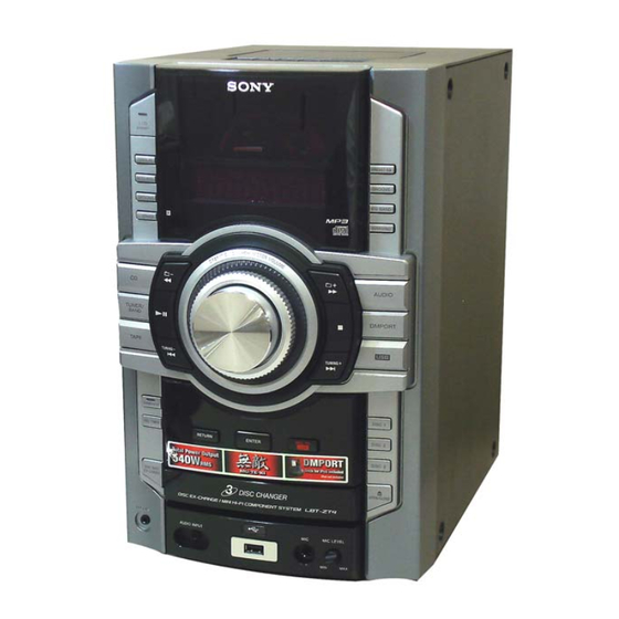
• HCD-ZT4 is the amplifi er, USB, CD player, tape
deck and tuner section in LBT-ZT4.
AUDIO POWER SPECIFICATION
POWER OUTPUT AND TOTAL
HARMONIC DISTORTION:
With 6 ohm loads, both channels driven,
from 120 Hz – 10 kHz; rated 110 watts per
channel minimum RMS power, with no
more than 0.7% total harmonic distortion
from 250 miliwatts to rated output.
Amplifier section
The following are measured at AC 120 V
60 Hz
Front speaker
RMS output power (reference):
180 W + 180 W (per channel at 6 ,
1 kHz, 10% THD)
Subwoofer
RMS output power (reference): 180 W
(at 6 , 100 Hz, 10% THD)
Inputs
AUDIO INPUT: sensitivity
800 mV, impedance 47 kilohms
MIC: sensitivity 1 mV, impedance
10 kilohms
(USB) port: Type A
DMPORT
Outputs
PHONES: accepts headphones of 8
more
FRONT SPEAKER: accepts impedance of
6
SUBWOOFER: accepts impedance of 6
Sony Corporation
9-889-196-01
2008F05-1
Audio Business Group
©
2008.06
Published by Sony Techno Create Corporation
CD
Section
Tape deck
Section
SPECIFICATIONS
USB section
Supported bit rate
MP3 (MPEG 1 Audio Layer-3):
32 – 320 kbps, VBR
WMA: 32 – 192 kbps, VBR
AAC: 48 – 320 kbps
Sampling frequencies
MP3 (MPEG 1 Audio Layer-3):
32/44.1/48 kHz
WMA: 44.1 kHz
AAC: 44.1 kHz
Transfer speed
Full-Speed
Supported USB device
Mass Storage Class
Maximum current
500 mA
CD player section
System: Compact disc and digital audio
system
Laser Diode Properties
Emission Duration: Continuous
Laser Output*: Less than 44.6 W
* This output is the value measurement
at a distance of 200 mm from the
objective lens surface on the Optical
Pick-up Block with 7 mm aperture.
Frequency response: 20 Hz – 20 kHz
or
Signal-to-noise ratio: More than 90 dB
Dynamic range: More than 88 dB
Tape deck section
Recording system: 4-track 2-channel, stereo
HCD-ZT4
Model Name Using Similar Mechanism
Mechanism Type
Optical Pick-up Block Name
Model Name Using Similar Mechanism
Tape Transport Mechanism Type
COMPACT DISC DECK RECEIVER
US Model
NEW
CDM88A-K6BD93-WOD
KSM-213DCP
NEW
TCM-J1 or CS-21SC-900TP
Tuner section
FM stereo, FM/AM superheterodyne tuner
FM tuner section
Tuning range:
87.5 – 108.0 MHz (100 kHz step)
Antenna: FM lead antenna
Antenna terminals: 75 ohms unbalanced
Intermediate frequency: 10.7 MHz
AM tuner section
Tuning range
530 – 1,710 kHz (with 10 kHz tuning
interval)
531 – 1,710 kHz (with 9 kHz tuning
interval)
Antenna: AM loop antenna, external antenna
terminal
Intermediate frequency: 450 kHz
General
Power requirements
AC 120 V,60 Hz
Power consumption
225 W
Dimensions (w/h/d) (excl. speakers)
Approx. 231 × 361 × 437.5 mm
(9 1/8 × 14 1/4 × 17 1/4 inch)
Mass (excl. speakers)
10.0 kg (22 lb 1 oz)
Design and specifications are subject to
change without notice.
Advertisement
Table of Contents

Related Manuals for Sony HCD-ZT4


Summary of Contents for Sony HCD-ZT4
-
Page 1: Specifications
HCD-ZT4 SERVICE MANUAL US Model Ver. 1.0 2008.06 • HCD-ZT4 is the amplifi er, USB, CD player, tape deck and tuner section in LBT-ZT4. Model Name Using Similar Mechanism Mechanism Type CDM88A-K6BD93-WOD Section Optical Pick-up Block Name KSM-213DCP Model Name Using Similar Mechanism... -
Page 2: Leakage Test
COMPONENTS IDENTIFIED BY MARK 0 OR DOTTED LINE WITH MARK 0 ON THE SCHEMATIC DIAGRAMS AND IN THE PARTS LIST ARE CRITICAL TO SAFE OPERATION. REPLACE THESE COMPONENTS WITH SONY PARTS WHOSE PART NUMBERS APPEAR AS SHOWN IN THIS MANUAL OR IN SUPPLEMENTS PUBLISHED BY SONY. -
Page 3: Table Of Contents
HCD-ZT4 TABLE OF CONTENTS SERVICING NOTES 7-10. Printed Wiring Board - USB Board - ......32 ..........7-11. Schematic Diagram - USB Board - ......... 33 7-12. Printed Wiring Board - DMPORT Board - ..... 34 GENERAL ..............7-13. Schematic Diagram - DMPORT Board - ......34 7-14. -
Page 4: Servicing Notes
HCD-ZT4 SECTION 1 SERVICING NOTES NOTES ON HANDLING THE OPTICAL PICK-UP BLOCK OR BASE UNIT The laser diode in the optical pick-up block may suffer electrostat- ic break-down because of the potential difference generated by the charged electrostatic load, etc. on clothing and the human body. - Page 5 HCD-ZT4 HOW TO OPEN THE TRAY WHEN POWER SWITCH TURN OFF Turn a gear by a driver till a lever falls down to the lever position of the figure. Pull the tray by the hand. gear hole HOW TO REMOVE THE KNOB VOLUME...
- Page 6 HCD-ZT4 CAPACITOR DISCHARGE FOR ELECTRIC SHOCK PREVENTION In checking the MAIN board, make a capacitor discharge of C803 and C804 for electric shock prevention. POWERAMP board C803 800 Ω/2W 800 Ω/2W POWERAMP board C804 CD MECHANISM BLOCK SERVICE POSITION CD mechanism block...
- Page 7 HCD-ZT4 POWERAMP BOARD SERVICE POSITION POWERAMP board MAIN board TRANS2 board front panel block CD mechanism block HOW TO DISTINGUISH TAPE MECHANISM DECK Two kinds of tape mechanism decks installed by this set exist. Please do the repair exchange after confi rming which tape mechanism deck set of the repair according to how to distinguish the fi gure below.
-
Page 8: General
HCD-ZT4 SECTION 2 This section is extracted GENERAL from instruction manual. Guide to parts and controls This manual mainly explains operations us ing the remote, but the same operations can also be performed using the buttons on the unit having the same or similar names. -
Page 9: Hooking Up The System Securely
HCD-ZT4 Remote RM-AMU008 +/– (select folder) TUNER MEMORY Press to select a folder. (on/standby) Press to preset the radio station. Press to turn on the system. +/– (tuning) Press to tune in the station you want. PLAY MODE/TUNING MODE CLEAR... -
Page 10: Disassembly
HCD-ZT4 SECTION 3 DISASSEMBLY • This set can be disassembled in the order shown below. 3-1. DISASSEMBLY FLOW 3-2. SIDE-L/R CASE (Page 11) 3-3. TOP PANEL BLOCK (Page 11) 3-5. FRONT PANEL BLOCK 3-4. TAPE MECHANISM DECK (Page 12) (Page 12) 3-6. -
Page 11: Side-L/R Case
HCD-ZT4 Note: Follow the disassembly procedure in the numerical order given. 3-2. SIDE-L/R CASE four screws (BVTP3 × 10) three screws (BVTP3 × 10) four screws (case 3 TP2) side-L case side-R case four screws (case 3 TP2) 3-3. TOP PANEL BLOCK screw (BVTP3 ×... -
Page 12: Tape Mechanism Deck
HCD-ZT4 3-4. TAPE MECHANISM DECK Note: This illustration is seeing top panel block from inside. two screws (BVTP2.6 × 8) bracket (deck) TC board two screws two screws (BVTP2.6 × 8) (BVTP3 × 8) connector (CN501) tape mechanism deck Cut the two clamps. -
Page 13: Dc Fan (M102), Back Panel
HCD-ZT4 3-6. DC FAN (M102), BACK PANEL DC fan (M102) power cord cord two screws bushing bracket bushing (BVTP3 × 12) two screws (BVTP3 × 10) coating clip screw (BVTP3 × 8) fan connector (CN690) two screws (BVTP3 × 10) screw (BVTP3 ×... -
Page 14: Cd Mechanism Block
HCD-ZT4 3-8. CD MECHANISM BLOCK screw (BVTP3 × 10) two screws (BVTP3 × 10) screw (BVTP3 × 10) two screws (BVTP3 × 10) wire (flat type) (31 core) (MAIN board: CN430/ CD board: CN201) screw (BVTP3 × 10) CD mechanism block... -
Page 15: Base Unit
HCD-ZT4 3-10. BASE UNIT two screws (PTPWHM2.6) insulator two springs two screws (PTPWHM2.6) (insulator) two polyethylene washers insulator two springs (insulator) base unit insulator insulator CD mechanism block – Bottom view – 3-11. OP BASE ASSY (KSM-213D) OP base assy... -
Page 16: Belt (Dlm3A)
HCD-ZT4 3-12. BELT (DLM3A) position of belt belt cover belt four screws two belts (DLM3A) -
Page 17: Test Mode
HCD-ZT4 SECTION 4 TEST MODE PANEL TEST MODE COMMON TEST MODE This mode is used to check the fl uorescent indicator tube, LEDs, This mode is used to check operations of the respective sections of keys, [MASTER VOLUME] jog, [OPERATION DIAL] jog, mod- Amplifi... - Page 18 HCD-ZT4 TUNER STEP CHANGE • Aging mode sequence: The step interval of AM channels can be toggled between 9 kHz START (from and 10 kHz. This mode is not available for Saudi Arabian, Euro- Disc 1) pean and Russian models.
- Page 19 HCD-ZT4 CD REPEATS 5 LIMIT OFF MODE Display of The number of repeat for CD playback is 5 times when the repeat Total Error mode is “REPEAT ALL”. This mode enables CD to repeat play- back for limitless times. Procedure: 1.
-
Page 20: Mechanical Adjustments
HCD-ZT4 SECTION 5 MECHANICAL ADJUSTMENTS VACS DISPLAY PRECAUTION 1. Clean the following parts with a denatured-alcohol-moistened This mode is used to check the VACS level. swab : Procedure: record/playback head pinch roller 1. Press [ ] button to turn on the system. -
Page 21: Electrical Adjustments
HCD-ZT4 SECTION 6 ELECTRICAL ADJUSTMENTS Adjustment Location: Record/Playback/Erase Head DECK SECTION 0 dB = 0.775V 1. Demagnetize the record/playback head with a head demagne- tizer. 2. Do not use a magnetized screwdriver for the adjustments. TEST TAPE Tape Signal Used for P-4-A063 6.3 kHz, -10 dB... - Page 22 HCD-ZT4 RF LEVEL CHECK TUNER SECTION oscilloscope FM TUNE LEVEL CHECK CD board signal TP123 (RFO) generator TP124 (VC) Procedure: Procedure: 1. Connect an oscilloscope to TP123 (RFO) and TP124 (VC). 1. Turn on the set. 2. Turn the power ON.
-
Page 23: Diagrams
HCD-ZT4 SECTION 7 DIAGRAMS 7-1. BLOCK DIAGRAM - CD SERVO, USB Section - DETECTOR +3.3V FNi1 (A) A/D CONVERTER IC501 97 FPi1 (B) (Page 24) CD-L AGCi RFEQo 81 RFi AINL 2 USB_REC-L (Page 24) STDO 94 FNi2 (C) 82 RFRPi... -
Page 24: Block Diagram - Main Section
HCD-ZT4 7-2. BLOCK DIAGRAM - MAIN Section - RV700 MIC LEVEL J700 MIC AMP MIC AMP IC700 (1/2) IC700 (2/2) (Page 25) HP IN 46 MIC J703 INPUT SELECTOR, ELECTRICAL VOLUME AUDIO INPUT IC407 LINE AMP AUX-L RECBL USB_REC-L IC251... -
Page 25: Block Diagram - Amp Section
HCD-ZT4 7-3. BLOCK DIAGRAM - AMP Section - HP IN (Page 24) J702 R-CH PHONES BASS AGC R-CH (Page 24) JK800 LINE AMP IC252 – (Page 24) FRONT – SPEAKER R-CH MUTING Q402 RY800 FAN MOTOR R-CH DRIVE M102 Q690, 691,... -
Page 26: Block Diagram - Panel, Power Supply Section
HCD-ZT4 7-4. BLOCK DIAGRAM - PANEL, POWER SUPPLY Section - PT901 MAIN POWER TRANSFORMER FLUORESCENT INDICATOR TUBE DRIVER SYSTEM CONTROLLER IC1101 IC401 (4/4) FLUORESCENT FL-DRIVER-DATA INDICATOR D908 TUBE –32V FL-DRIVER-CLK –VFL REGULATOR DR35 - DR16 FL-DRIVER-CS FL1101 Q902 RSTB FL-DRIVER-RESET... - Page 27 HCD-ZT4 THIS NOTE IS COMMON FOR PRINTED WIRING BOARDS AND SCHEMATIC DIAGRAMS. • Circuit Boards Location (In addition to this, the necessary note is printed in each block.) TRANS2 board For Printed Wiring Boards. For Schematic Diagrams. Note: Note: 9V REG board TC board •...
-
Page 28: Schematic Diagram - Cd Board (1/2)
HCD-ZT4 7-5. SCHEMATIC DIAGRAM - CD Board (1/2) - • See page 34 for waveforms. • See page 52 for IC Pin Function Description. (1/2) C112 R118 C108 C107 100k C153 C136 R108 R114 R139 R109 R143 R142 R140 R130 4.7k... -
Page 29: Schematic Diagram - Cd Board (2/2)
HCD-ZT4 7-6. SCHEMATIC DIAGRAM - CD Board (2/2) - • See page 50 for IC Block Diagrams. (2/2) R510 A/D CONVERTER C510 C511 IC501 AK5358A R511 STDO DGND C507 LRCK DATA SELECTOR R512 MCLK C506 SCLK AGND C505 R508 VCOM... -
Page 30: Printed Wiring Board - Cd Board
HCD-ZT4 7-7. PRINTED WIRING BOARD - CD Board - • See page 27 for Circuit Boards Location. • : Uses unleaded solder. CD BOARD (CONDUCTOR SIDE) CD BOARD (COMPONENT SIDE) (SPINDLE) (LIMIT) (SLED) TP124 R135 (VC) R225 TP123 (RFO) R226... -
Page 31: Printed Wiring Board - Tc Board
HCD-ZT4 7-9. SCHEMATIC DIAGRAM - TC Board - 7-8. PRINTED WIRING BOARD - TC Board - • See page 34 for Waveforms. • See page 27 for Circuit Boards Location. • : Uses unleaded solder. TC BOARD C546 R506 R544... -
Page 32: Printed Wiring Board - Usb Board
HCD-ZT4 7-10. PRINTED WIRING BOARD - USB Board - • See page 27 for Circuit Boards Location. • : Uses unleaded solder. USB BOARD (CONDUCTOR SIDE) USB BOARD (COMPONENT SIDE) R928 R921 C901 IC915 C914 R938 RB922 RB921 R945 R937... -
Page 33: Schematic Diagram - Usb Board
HCD-ZT4 7-11. SCHEMATIC DIAGRAM - USB Board - • See page 34 for Waveforms. • See page 50 for IC Block Diagrams. • See page 52 for IC Pin Function Description. S-RAM IC921 IS61LV6416-10T C912 C910 C909 R916 CN907 R970... -
Page 34: Printed Wiring Board - Dmport Board
HCD-ZT4 • Waveforms 7-12. PRINTED WIRING BOARD - DMPORT Board - • See page 27 for Circuit Boards Location. • : Uses unleaded solder. – CD Board – – TC Board – – MAIN Board – IC101 (FEi) L501 IC401... -
Page 35: Printed Wiring Board - Main Board
HCD-ZT4 7-14. PRINTED WIRING BOARD - MAIN Board - • See page 27 for Circuit Boards Location. • : Uses unleaded solder. • Semiconductor Location Ref. No. Location Ref. No. Location (Page 44) DISPLAY D110 Q113 BOARD CN1101 D116 Q115... -
Page 36: Schematic Diagram - Main Board (1/4)
HCD-ZT4 7-15. SCHEMATIC DIAGRAM - MAIN Board (1/4) - • See page 50 for IC Block Diagrams. MAIN BOARD (1/4) ET601 CN490 C241 ET602 1000p CHASSIS GND C648 220p PGND (CHASSIS) C280 C647 DMPORT+5V DMPORT-L R129 2.2k C294 220p 0.015 R179 2.2k... -
Page 37: Schematic Diagram - Main Board (2/4)
HCD-ZT4 7-16. SCHEMATIC DIAGRAM - MAIN Board (2/4) - • See page 34 for Waveforms. • See page 52 for IC Pin Function Description. MAIN BOARD (2/4) MAIN BOARD C576 (4/4) (Page 39) D468 R483 MA2J1110GLS0 220k R463 R357 D695... -
Page 38: Schematic Diagram - Main Board (3/4)
HCD-ZT4 7-17. SCHEMATIC DIAGRAM - MAIN Board (3/4) - MAIN BOARD (3/4) NO458 D630 MA2J1110GLS0 JL234 UNREG C605 0.01 JL235 JL236 REG_PROTECT 0.01 C617 5V REG DMPORT+5V C618 BOARD MAIN 0.01 CN055 BOARD DMPORT ON/OFF (2/4) (Page 43) (Page 37) -
Page 39: Schematic Diagram - Main Board (4/4)
HCD-ZT4 7-18. SCHEMATIC DIAGRAM - MAIN Board (4/4) - • See page 50 for IC Block Diagrams. MAIN BOARD (4/4) MAIN MAIN BOARD BOARD (2/4) (3/4) IC673 IC B/D (Page 37) (Page 38) DATA SELECTOR IC673 TC74VHC157FT(EKJ) R666 Q655-658 1.5k... -
Page 40: Printed Wiring Board - Poweramp Board
HCD-ZT4 7-19. PRINTED WIRING BOARD - POWERAMP Board - • See page 27 for Circuit Boards Location. • : Uses unleaded solder. • Semiconductor Location POWERAMP BOARD Ref. No. Location D800 D801 D802 D803 D804 R848 D805 D806 D810 D807... -
Page 41: Schematic Diagram - Poweramp Board
HCD-ZT4 7-20. SCHEMATIC DIAGRAM - POWERAMP Board - POWERAMP BOARD IC800 POWER AMP IC800 STK416-120-E +PRE SUB GND R833 0.22 C826 R865 100V R835 2.2k R832 0.22 R831 0.22 L801 1.7uH RY800 JK800 R840 R808 10 R810 R80910 FRONT L802 1.7uH... -
Page 42: Printed Wiring Boards - Jack Section
HCD-ZT4 7-21. PRINTED WIRING BOARDS - JACK Section - 7-22. SCHEMATIC DIAGRAM - JACK Section - • See page 27 for Circuit Boards Location. • : Uses unleaded solder. JK890 J700 J702 SUBWOOFER PHONES SW JACK BOARD MIC BOARD C718... -
Page 43: Printed Wiring Boards - Reg Section
HCD-ZT4 7-23. PRINTED WIRING BOARDS - REG Section - 7-24. SCHEMATIC DIAGRAM - REG Section - • See page 50 for IC Block Diagrams. • See page 27 for Circuit Boards Location. • : Uses unleaded solder. 5V REG BOARD... -
Page 44: Printed Wiring Boards - Display Board
HCD-ZT4 7-25. PRINTED WIRING BOARD - DISPLAY Board - • See page 27 for Circuit Boards Location. • : Uses unleaded solder. • Semiconductor Location DISPLAY BOARD Ref. No. Location D1124 R1171 R1172 D1125 D1196,S1165 D1126 TUNER/ TAPE BAND D1205,S1193... -
Page 45: Schematic Diagram - Display Board
HCD-ZT4 7-26. SCHEMATIC DIAGRAM - DISPLAY Board - • See page 50 for IC Block Diagrams. DISPLAY BOARD FL1101 TP0045 SEL A FLUORESCENT INDICATOR TUBE TP0044 SEL B TP0043 METER LED CTRL TP0042 DGND FFC001 TP0041 METER SW TP0040 MGND... -
Page 46: Printed Wiring Boards - Panel Section
HCD-ZT4 7-27. PRINTED WIRING BOARDS - PANEL Section - • See page 27 for Circuit Boards Location. • : Uses unleaded solder. • Semiconductor Location Ref. No. Location D011 SW BOARD D012 D013 R031 D014 MOTOR DRIVE BOARD D015 S031... -
Page 47: Schematic Diagram - Panel Section
HCD-ZT4 7-28. SCHEMATIC DIAGRAM - PANEL Section - • See page 50 for IC Block Diagrams. MOTOR DRIVE BOARD CN002 IC001 IC B/D TP12 (METER) OUT3 C001 MOTOR DRIVE TP13 IC001 OUT1 CN001 LB1846M TP14 OUT2 TP01 TP15 C002 SW BOARD... -
Page 48: Printed Wiring Board - Trans2 Board
HCD-ZT4 7-29. PRINTED WIRING BOARD - TRANS2 Board - • See page 27 for Circuit Boards Location. • : Uses unleaded solder. • Semiconductor Location Q903 Ref. No. Location R915 D901 R904 R904 D901 Q902 C909 D906 RY901 F908 D908... -
Page 49: Schematic Diagram - Trans2 Board
HCD-ZT4 7-30. SCHEMATIC DIAGRAM - TRANS2 Board - TRANS2 BOARD JL921 PT901 MAIN POWER F909 C908 TRANSFORMER T8AL JW907 250V JL919 CN903 F905 JL901 JL920 T6.3AL AC-VH 250V JL933 AC-VL JL934 F904 JL935 RY901 T6.3AL POWERAMP 250V BOARD JL904 (2/2) - Page 50 HCD-ZT4 • IC Block Diagrams IC401 BA5826SFP-E2 – MAIN Board – IC407 R2A15216FP – CD Board – VO1(–) IC201 TK63115SCL-G@GT D.BUFF VO4(–) VO1(+) D.BUFF LEVEL D.BUFF VIN 1 VO4(+) SHIFT D.BUFF THERMAL & LEVEL OVER CURRENT SHIFT PROTECTION INDR REFERENCE...
-
Page 51: Display Board
HCD-ZT4 – 5V REG Board – IC055 BA00BC0WCP-V5E2 VREF – DRIVER THERMAL OVER CURRENT SHUT DOWN PROTECT – DISPLAY Board – IC1101 NJU3427FH2 51 50 49 48 46 45 RESET SERIAL CIRCUIT BUFFER INSTRUCTION TIMING DUTY DECODER COUNTER COUNTER ADDRESS... - Page 52 HCD-ZT4 • IC Pin Function Description CD BOARD IC101 TC94A70FG-101 (CD-MP3 PROCESSOR) Pin No. Pin Name Description AVSS3 Ground terminal RFZi RF ripple zero crossing signal input terminal RFRP RF ripple signal output terminal SBAD/RFDC Sub beam addition signal or RF peak detection signal output terminal...
- Page 53 HCD-ZT4 Pin No. Pin Name Description SBOK/FOK Not used Not used SFSY/LOCK Not used ZDET Zero detection signal output terminal Not used GPIN Not used Microcomputer interface mode selection signal input terminal Fixed at "H" in this set DOUT (PO6)
- Page 54 HCD-ZT4 USB BOARD IC901 TMP92CD28AFG-7AC9 (USB CONTROLLER) Pin No. Pin Name Description /RESET Reset signal input from the system controller "L": reset Ready to send signal input from the system controller 3, 4 NO USE Not used Function selection signal input terminal Fixed at "L"...
- Page 55 HCD-ZT4 Pin No. Pin Name Description Two-way EEPROM IIC clock bus terminal Not used Bit clock signal output to the CD-MP3 processor DATA Audio data output to the CD-MP3 processor GATE Gate signal output to the CD-MP3 processor DVCC Power supply terminal (+3.3 V)
- Page 56 HCD-ZT4 MAIN BOARD IC401 R5F3640MDFAR (SYSTEM CONTROLLER) Pin No. Pin Name Description METER-IN3, 1, 2 Meter motor drive signal output to the motor drive METER-IN4 SW LED LED drive signal output terminal for SUBWOOFER indicator SIRCS SIRCS signal input from the remote control receiver...
- Page 57 HCD-ZT4 Pin No. Pin Name Description ST-TUNED Tuned detection input from the tuner (FM/AM) Power supply terminal (+3.3V) ST-CE PLL chip enable signal output to the tuner (FM/AM) Ground terminal ST-DIN PLL serial data output to the tuner (FM/AM) ST-CLK...
-
Page 58: Exploded Views
HCD-ZT4 SECTION 8 EXPLODED VIEWS Note: When indicating parts by reference num- • -XX and -X mean standardized parts, so • The mechanical parts with no reference ber, please include the board name. they may have some difference from the number in the exploded views are not sup- original one. -
Page 59: Loading Panel Section
HCD-ZT4 8-2. LOADING PANEL SECTION back panel section DISPLAY BOARD section Ref. No. Part No. Description Remark Ref. No. Part No. Description Remark 3-283-215-81 PANEL, LOADING 7-685-647-79 SCREW +BVTP 3X10 TYPE2 IT-3 1-543-793-11 FILTER, CLAMP (FERRITE CORE) -
Page 60: Display Board Section
HCD-ZT4 8-3. DISPLAY BOARD SECTION meter display panel assy FFC001 not supplied (VOLUME board) S1051 DISPLAY board supplied supplied with S1051 front panel section Ref. No. Part No. Description Remark Ref. No. Part No. Description Remark 3-283-207-01 KNOB JOG A-1444-627-A... -
Page 61: Front Panel Section
HCD-ZT4 8-4. FRONT PANEL SECTION not supplied (MINI JACK board) not supplied not supplied not supplied not supplied not supplied (MIC board) Ref. No. Part No. Description Remark Ref. No. Part No. Description Remark X-2188-450-2 FRONT PANEL ASSY A-1444-543-A USB CONNECTOR BOARD, COMPLETE... -
Page 62: Meter Display Assy
HCD-ZT4 8-5. METER DISPLAY ASSY not supplied (LED board) not supplied not supplied not supplied (MOTOR DRIVE board) supplied not supplied supplied supplied not supplied not supplied not supplied not supplied (SW board) Ref. No. Part No. Description Remark Ref. No. -
Page 63: Top Panel Section
HCD-ZT4 8-6. TOP PANEL SECTION not supplied not supplied not supplied TC board FFC502 not supplied Note: When you exchange Ref. No. 260, 261 or 262, Please refer to “HOW TO DISTINGUISH TAPE MECHANISM DECK” of the service note (6 page). -
Page 64: Back Panel Section
HCD-ZT4 8-7. BACK PANEL SECTION M102 supplied not supplied M101 supplied not supplied (5V REG board) not supplied (SW JACK board) IC055 not supplied IC050 not supplied not supplied (DMPORT board) MAIN BOARD section not supplied (USB board) Ref. No. -
Page 65: Main Board Section
HCD-ZT4 8-8. MAIN BOARD SECTION not supplied (9V REG board) not supplied not supplied FFC220 MAIN chassis section board Ref. No. Part No. Description Remark Ref. No. Part No. Description Remark A-1444-635-A MAIN BOARD, COMPLETE FFC220 1-835-392-21 WIRE (FLAT TYPE) (9 CORE) -
Page 66: Chassis Section
HCD-ZT4 8-9. CHASSIS SECTION not supplied (TRANS2 board) F908 F904 F905 F909 F907 F906 PT901 not supplied not supplied (BU FFC board) not supplied CD mechanism section supplied Ref. No. Part No. Description Remark Ref. No. Part No. Description Remark... -
Page 67: Cd Mechanism Section (Cdm88A-K6Bd93-Wod)
HCD-ZT4 8-10. CD MECHANISM SECTION (CDM88A-K6BD93-WOD) not supplied (including sled motor (M402), spindle motor (M401)) not supplied sled motor (M402) spindle motor (M401) S201 Ref. No. Part No. Description Remark Ref. No. Part No. Description Remark 1-797-193-31 MECHANICAL, CD (DLM3A) -
Page 68: Electrical Parts List
HCD-ZT4 SECTION 9 5V REG 9V REG ELECTRICAL PARTS LIST Note: • Due to standardization, replacements in • RESISTORS When indicating parts by reference num- the parts list may be different from the All resistors are in ohms. ber, please include the board name. - Page 69 HCD-ZT4 Ref. No. Part No. Description Remark Ref. No. Part No. Description Remark C148 1-162-923-11 CERAMIC CHIP 47PF R114 1-216-833-11 METAL CHIP 1/10W C149 1-162-919-11 CERAMIC CHIP 22PF R118 1-216-845-11 METAL CHIP 100K 1/10W C150 1-162-964-11 CERAMIC CHIP 0.001uF R120...
- Page 70 HCD-ZT4 DISPLAY Ref. No. Part No. Description Remark Ref. No. Part No. Description Remark R508 1-216-841-11 METAL CHIP 1/10W Q1139 8-729-620-07 TRANSISTOR 2SC3052EF-T1-LEF R509 1-216-845-11 METAL CHIP 100K 1/10W Q1141 8-729-620-07 TRANSISTOR 2SC3052EF-T1-LEF R510 1-216-821-11 METAL CHIP 1/10W Q1143 8-729-620-07...
- Page 71 HCD-ZT4 DISPLAY DMPORT Ref. No. Part No. Description Remark Ref. No. Part No. Description Remark R1192 1-216-827-11 METAL CHIP 3.3K 1/10W R1193 1-216-829-11 METAL CHIP 4.7K 1/10W C1309 1-107-826-11 CERAMIC CHIP 0.1uF R1194 1-218-867-11 METAL CHIP 6.8K 0.5% 1/10W C1310...
- Page 72 HCD-ZT4 MAIN Ref. No. Part No. Description Remark Ref. No. Part No. Description Remark R015 1-216-817-11 METAL CHIP 1/10W C194 1-126-964-11 ELECT 10uF R016 1-216-816-11 METAL CHIP 1/10W R017 1-216-816-11 METAL CHIP 1/10W C195 1-126-964-11 ELECT 10uF R019 1-216-821-11 METAL CHIP...
- Page 73 HCD-ZT4 MAIN Ref. No. Part No. Description Remark Ref. No. Part No. Description Remark C483 1-162-964-11 CERAMIC CHIP 0.001uF < DIODE > C496 1-100-597-91 CERAMIC CHIP 0.1uF D110 6-501-772-01 DIODE MAZ8130GMLS0 C498 1-126-964-11 ELECT 10uF D116 6-501-579-01 DIODE MC2837 C499 1-100-597-91 CERAMIC CHIP 0.1uF...
- Page 74 HCD-ZT4 MAIN Ref. No. Part No. Description Remark Ref. No. Part No. Description Remark JR115 1-216-296-11 SHORT CHIP Q690 8-729-620-07 TRANSISTOR 2SC3052EF-T1-LEF JR116 1-216-296-11 SHORT CHIP Q691 8-729-620-07 TRANSISTOR 2SC3052EF-T1-LEF JR117 1-216-296-11 SHORT CHIP Q693 8-729-620-07 TRANSISTOR 2SC3052EF-T1-LEF Q694 8-729-620-07...
- Page 75 HCD-ZT4 MAIN Ref. No. Part No. Description Remark Ref. No. Part No. Description Remark R201 1-216-841-11 METAL CHIP 1/10W R328 1-216-837-11 METAL CHIP 1/10W R202 1-216-809-11 METAL CHIP 1/10W R345 1-216-833-11 METAL CHIP 1/10W R203 1-216-817-11 METAL CHIP 1/10W R346...
- Page 76 HCD-ZT4 MAIN Ref. No. Part No. Description Remark Ref. No. Part No. Description Remark R610 1-216-845-11 METAL CHIP 100K 1/10W R696 1-216-829-11 METAL CHIP 4.7K 1/10W R612 1-216-801-11 METAL CHIP 1/10W R697 1-216-845-11 METAL CHIP 100K 1/10W R613 1-216-825-11 METAL CHIP 2.2K...
- Page 77 HCD-ZT4 MINI JACK MOTOR DRIVE POWERAMP Ref. No. Part No. Description Remark Ref. No. Part No. Description Remark R718 1-216-836-11 METAL CHIP 1/10W A-1444-632-A POWERAMP BOARD, COMPLETE R719 1-216-833-11 METAL CHIP 1/10W ************************** R720 1-216-845-11 METAL CHIP 100K 1/10W 7-685-646-79...
- Page 78 HCD-ZT4 POWERAMP Ref. No. Part No. Description Remark Ref. No. Part No. Description Remark < JACK > R836 1-216-837-11 METAL CHIP 1/10W R837 1-216-837-11 METAL CHIP 1/10W JK800 1-820-067-11 TERMINAL BOARD (SPEAKER) R838 1-216-845-11 METAL CHIP 100K 1/10W R839 1-216-845-11...
- Page 79 HCD-ZT4 SW JACK Ref. No. Part No. Description Remark Ref. No. Part No. Description Remark SW BOARD C513 1-126-960-11 ELECT ********* C514 1-126-960-11 ELECT C515 1-126-947-11 ELECT 47uF < RESISTOR > C516 1-126-947-11 ELECT 47uF C517 1-162-964-11 CERAMIC CHIP 0.001uF...
- Page 80 HCD-ZT4 TRANS2 Ref. No. Part No. Description Remark Ref. No. Part No. Description Remark < RESISTOR > C926 1-100-597-91 CERAMIC CHIP 0.1uF R501 1-216-825-11 METAL CHIP 2.2K 1/10W < CONNECTOR > R502 1-216-825-11 METAL CHIP 2.2K 1/10W R503 1-216-825-11 METAL CHIP 2.2K...
- Page 81 HCD-ZT4 USB CONNECTOR Ref. No. Part No. Description Remark Ref. No. Part No. Description Remark C907 1-107-826-11 CERAMIC CHIP 0.1uF R923 1-216-802-11 METAL CHIP 1/10W C908 1-107-826-11 CERAMIC CHIP 0.1uF R924 1-216-802-11 METAL CHIP 1/10W C909 1-162-919-11 CERAMIC CHIP 22PF...
- Page 82 HCD-ZT4 USB CONNECTOR VOLUME Ref. No. Part No. Description Remark < RESISTOR > R1001 1-216-821-11 METAL CHIP 1/10W R1002 1-216-821-11 METAL CHIP 1/10W R1004 1-216-821-11 METAL CHIP 1/10W R1005 1-216-821-11 METAL CHIP 1/10W ************************************************************ VOLUME BOARD ************* < RESISTOR >...
- Page 83 HCD-ZT4 MEMO...
-
Page 84: Revision History
HCD-ZT4 REVISION HISTORY Checking the version allows you to jump to the revised page. Also, clicking the version at the top of the revised page allows you to jump to the next revised page. Ver. Date Description of Revision 2008.06...
Need help?
Do you have a question about the HCD-ZT4 and is the answer not in the manual?
Questions and answers