Table of Contents
Advertisement
SERVICE MANUAL
Ver. 1.1 2008.07
• HCD-GZR7D/GZR8D/GZR9D are the
tuner, deck, DVD and amplifi er section
in MHC-GZR7D/GZR8D/GZR9D.
Amplifi er Section
The following measured at AC 230 V, 50/60 Hz (Russian model)
The following measured at AC 127, 220, 240 V, 50/60 Hz
(Saudi Arabian model)
The following measured at AC 120, 220, 240 V, 50/60 Hz (Other models)
MHC-GZR9D
Power output (rated): 100 W + 100 W (6 Ω at 1 kHz, 1% THD)
RMS output power (reference)
180 W + 180 W (per channel at 6 Ω, 1 kHz,
Front speaker:
10% THD)
60 W (6 Ω at 1 kHz, 10% THD)
Center speaker:
60 W + 60 W (per channel at 6 Ω, 1 kHz,
Surround speaker:
10% THD)
180 W (6 Ω at 80 Hz, 10% THD)
Subwoofer:
MHC-GZR8D
Power output (rated): 100 W + 100 W (6 Ω at 1 kHz, 1% THD)
RMS output power (reference)
180 W + 180 W (per channel at 6 Ω, 1 kHz,
Front speaker:
10% THD)
60 W (6 Ω at 1 kHz, 10% THD)
Center speaker:
60 W + 60 W (per channel at 6 Ω, 1 kHz,
Surround speaker:
10% THD)
Sony Corporation
9-889-156-02
2008G04-1
Audio&Video Business Group
©
2008.07
Published by Sony Techno Create Corporation
HCD-GZR7D/GZR8D/
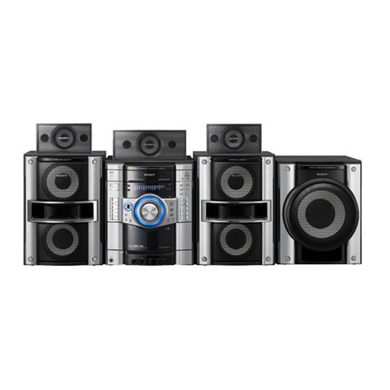
Photo: HCD-GZR8D
Model Name Using Similar Mechanism
DVD
DVD Mechanism Type
Section
Optical Pick-up Name
Tape Deck
Model Name Using Similar Machanism
Section
SPECIFICATIONS
MHC-GZR7D
Power output (rated): 100 W + 100 W (6 Ω at 1 kHz, 1% THD)
RMS output power (reference):
Inputs
VIDEO/SAT VIDEO IN (phono jack):
VIDEO/SAT AUDIO IN L/R (phono jacks):
MIC 1/MIC 2 (phone jacks):
GZR9D
E Model
HCD-GZR7D/GZR8D/GZR9D
Australian Model
Russian Model
HCD-GZR7D/GZR9D
HCD-GNZ777D/GNZ888D
CDM74HF-DVBU101//C
KHM-313CAB/C2RP
HCD-GNZ777D/GNZ888D
180 W+ 180 W (per channel at 6 Ω, 1 kHz,
10% THD)
1 Vp-p, 75 ohms
voltage 250/450 mV, impedance 47 kilohms
sensitivity 1 mV, impedance 10 kilohms
– Continued on next page –
DVD DECK RECEIVER
HCD-GZR9D
Advertisement
Table of Contents

Related Manuals for Sony HCD-GZR9D


Summary of Contents for Sony HCD-GZR9D
-
Page 1: Service Manual
60 W (6 Ω at 1 kHz, 10% THD) Center speaker: 60 W + 60 W (per channel at 6 Ω, 1 kHz, Surround speaker: 10% THD) DVD DECK RECEIVER Sony Corporation 9-889-156-02 2008G04-1 Audio&Video Business Group © 2008.07 Published by Sony Techno Create Corporation... - Page 2 COMPONENTS IDENTIFIED BY MARK 0 OR DOTTED LINE WITH MARK 0 ON THE SCHEMATIC DIAGRAMS AND IN THE PARTS LIST ARE CRITICAL TO SAFE OPERATION. REPLACE THESE COMPONENTS WITH SONY PARTS WHOSE PART NUMBERS APPEAR AS SHOWN IN THIS MANUAL OR IN SUPPLEMENTS PUBLISHED BY SONY.
- Page 3 HCD-GZR7D/GZR8D/GZR9D NOTES ON LASER DIODE EMISSION CHECK NOTES ON CHIP COMPONENT REPLACEMENT • Never reuse a disconnected chip component. The laser beam on this model is concentrated so as to be focused • Notice that the minus side of a tantalum capacitor may be dam- on the disc refl...
- Page 4 HCD-GZR7D/GZR8D/GZR9D Ver. 1.1 MODEL IDENTIFICATION – Back Panel – Parts No. Model Parts No. GZR9D: RU 3-285-875-0[] GZR9D: E3, E15 3-285-875-1[] GZR9D: EA 3-285-875-2[] GZR9D: SP 3-285-875-4[] GZR9D: PH 3-285-875-6[] GZR9D: E2 3-285-875-7[] GZR9D: AUS 3-285-875-8[] GZR9D: AR 3-285-875-9[] GZR8D: E3, E15 3-291-798-1[] GZR8D: EA 3-291-798-2[]...
-
Page 5: Table Of Contents
HCD-GZR7D/GZR8D/GZR9D Ver. 1.1 TABLE OF CONTENTS SERVICING NOTES 7-6. Printed Wiring Boards –Driver Section– ......49 ..........7-7. Schematic Diagram –Driver Section– ......50 7-8. Printed Wiring Board –DMB18 Board (1/2)– ....51 GENERAL 7-9. Printed Wiring Board –DMB18 Board (2/2)– ....52 Guide to parts and controls .......... -
Page 6: Servicing Notes
HCD-GZR7D/GZR8D/GZR9D SECTION 1 SERVICING NOTES Notes on Disconnecting Between the OP Section (DVBU101) and the DMB18 Board Note: When disconnecting between the OP section (DVBU101) and the DMB18 board, be sure to make a solder brige for electrostatic prevention as illustrated in the fi gure (before disconnection). On the contrary, when installing the OP section, never remove the solder bride until the OP section and the DMB18 board are connected. - Page 7 HCD-GZR7D/GZR8D/GZR9D Notes on Installing the Two Cooling Fans (FAN901 and FAN902) (HCD-GZR8D/GZR9D) Note: The HCD-GZR8D/GZR9D has two cooling fans (FAN901 and FAN902) used. The connectors of these fans have the same color and the same number of pins. When installing these fans, check the marking of CN601 and CN602 on the MAIN board and ensure that they are located correctly. The CN601 on the MAIN board is to be attached with the connector of FAN901 where as the CN602 is to be attached with the connector of FAN902.
-
Page 8: General
HCD-GZR7D/GZR8D/GZR9D SECTION 2 This section is extracted GENERAL from instruction manual. Guide to parts and controls also be performed using the buttons on the unit having the same or similar names. Unit... - Page 9 HCD-GZR7D/GZR8D/GZR9D Remote (on/standby) (24, 79, 106, 129) Unit: STANDBY indicator (118) Remote: TV / (on/standby) (29) DISPLAY (27, 33, 73, 107, 108) Press to display the disc information or clock in the front panel display. Unit: ILLUMINATION (108, 129) Press to change the illumination pattern around MASTER VOLUME Display Disc tray...
- Page 10 HCD-GZR7D/GZR8D/GZR9D ENTER (28, 33, 34, 39, 44, 49, 53, OPTIONS (74, 75, 107, 116) 58, 59, 60, 63, 71, 74, 76, 79, 83, Press to enter the option menus. 87, 95, 102, 105, 129) Press to enter the settings. Unit: OPEN/CLOSE (38) Press to load or eject a disc.
- Page 11 HCD-GZR7D/GZR8D/GZR9D (stop) (39, 72, 75, 79) MIC 1/MIC 2 jacks (77, 98) Press to stop playback. Connect a microphone. (rewind/fast forward) MIC 1 LEVEL/MIC 2 LEVEL (98) (39, 75) Turn to adjust the microphone volume. ECHO LEVEL (99) Unit: (39) Turn to adjust the echo level.
- Page 12 HCD-GZR7D/GZR8D/GZR9D (MHC-GZR9D only) Unit: DVD (26, 27, 34, 38, 76, 79, SUBWOOFER (30) Press to select the “DVD” function. SUBWOOFER indicator (30) Unit: USB (76, 81, 85, 98) Lights up when the subwoofer is turned Press to select the “USB” function. Unit: TAPE A/B (74, 75) PICTURE NAVI (54, 89) Press to select the “TAPE”...
- Page 13 HCD-GZR7D/GZR8D/GZR9D ANGLE (40) RETURN (43, 53, 59, 81, 88) Press to change the angle (DVD VIDEO Press to return to the previous menu on with multi-angles only). the TV screen. DVD/TUNER MENU (49, 52, 58, / / / (28, 29, 44, 45, 49, 71, 71, 87) 80, 96, 105) Press to select the menu items.
- Page 14 Press to activate the “THEATRE SYNC” vocal score. function. KARAOKE MODE (99) Press to select the Karaoke mode. details, see “Operating a Sony TV” (page 29). , TV VOL + KARAOKE PON (101) VOLUME + buttons on the remote have a tactile dot. Use the tactile dot Press to activate the “Karaoke Pon”...
- Page 15 HCD-GZR7D/GZR8D/GZR9D Display Lights up when the output video Lights up during transfer or signal is NTSC. (27) recording. (75, 78, 83) Indicates the current surround Indicates the tape playback direction. format. (74) Lights up when disc number is Displays the text information. displayed.
- Page 16 HCD-GZR7D/GZR8D/GZR9D MHC-GZR8D Hooking up optional components To enhance your system, you can connect optional components. Refer to the operating instructions provided with each component. Rear panel MHC-GZR9D MHC-GZR7D Continued...
- Page 17 HCD-GZR7D/GZR8D/GZR9D VIDEO/SAT AUDIO IN L/R jacks S VIDEO OUT jack Connect the audio output jacks of an Connect the S Video input jack of the optional component (such as VCR or TV or projector. You can enjoy higher satellite tuner). quality video images when you select the S VIDEO.
- Page 18 HCD-GZR7D/GZR8D/GZR9D D-LIGHT SYNC OUT jack DVD DIGITAL OUT jack (MHC- (Except for Russian and GZR7D only) Australian models) Connect the digital optical input jack of an optional digital component Connect the D-LIGHT SYNC controller (not supplied). You need 5.1 channel sound, if the connected to connect the D-LIGHT SYNC controller to the lighting device* (not or DTS decoder.
-
Page 19: Disassembly
HCD-GZR7D/GZR8D/GZR9D SECTION 3 DISASSEMBLY • This set can be disassembled in the order shown below. 3-19. VIDEO BOARD 3-1. CASE (Page 29) (Page 20) 3-2. LOADING PANEL (Page 20) 3-20. DMB18 BOARD 3-21. DVD ASSY (Page 29) (Page 30) 3-3. TUNER PACK, DMPORT BOARD 3-23. -
Page 20: Case
HCD-GZR7D/GZR8D/GZR9D Note: Follow the disassembly procedure in the numerical order given. 3-1. CASE case screw (case 3 TP2) screw screw (case 3 TP2) (case 3 TP2) seven screws (+BVTP 3 × 8) screw (case 3 TP2) 3-2. LOADING PANEL loading panel CD mechanism deck (CDM74) Turn the pulley to the direction of the arrow. -
Page 21: Tuner Pack, Dmport Board
HCD-GZR7D/GZR8D/GZR9D 3-3. TUNER PACK, DMPORT BOARD DMPORT board two screws CN203 (2P) (+BVTP 3 × 8) tuner pack wire (flat type)(9 core) (CN201) two screws (+BVTP 3 × 6) connector (9 core) 3-4. DVD BLOCK SECTION wire DVD block section screw (+BVTP 3 ×... -
Page 22: Front Panel Section
HCD-GZR7D/GZR8D/GZR9D 3-5. FRONT PANEL SECTION CN073 (2P) front panel section wire (flat type)(11 core) (CN103) CN301 (3P) CN302 (8P) wire (flat type)(29 core) (CN402) wire (flat type)(9 core) (CN101) four screws (+BVTP 3 × 8) 3-6. SUB-TRANS BOARD SUB-TRANS board CN911 (4P) three screws CN901 (2P) -
Page 23: Back Panel Section
HCD-GZR7D/GZR8D/GZR9D 3-7. BACK PANEL SECTION CN602 (3P) CN601 (3P) CN448 (4P) (HCD-GZR9D) CN447 (9P) four screws (+BVTP 3 × 8) CN544 (6P) (HCD-GZR8D/GZR9D) screw (+BVTP 3 × 8) back panel section five screws (+BVTP 3 × 8) 3-8. BOARDS SECTION... -
Page 24: Surr & Cent Amp Board
HCD-GZR7D/GZR8D/GZR9D 3-9. SURR & CENT AMP BOARD (HCD-GZR8D/GZR9D) two screws SURR & CENT AMP board (transistor) CN444 (7P) screw (+BVTP 3 × 8) bracket (PWB AMP) screw (+BVTP 3 × 8) two screws (+BVTP 3 × 8) duct (fan) 3-10. MAIN BOARD MAIN board screw (+BVTP 3 ×... -
Page 25: Regulator Board
HCD-GZR7D/GZR8D/GZR9D 3-11. REGULATOR BOARD four screws (+BVTP 3 × 8) REGULATOR board AMP FR & SW board 3-12. AMP FR & SW BOARD two screws (transister) screw (+BVTP 3 × 8) bracket (PWB AMP-B) screw (+BVTP 3 × 8) screw (+BVTP 3 ×... -
Page 26: Tape Mechanism Deck
HCD-GZR7D/GZR8D/GZR9D 3-13. TAPE MECHANISM DECK front panel assy wire two screws (+BVTP 2.6 (3CR)) two screws (+BVTP 2.6 (3CR)) two screws (+BVTP 2.6 (3CR)) tape mechanism deck 3-14. MIC BOARD, HEADPHONE BOARD front panel assy three knobs (MIC) HEADPHONE board HP HLDR board screw (+BVTP 2.6 (3CR)) -
Page 27: Lid (Tc-L), Lid (Tc-R)
VOLUME board three screws (+BVTP 2.6 (3CR)) knob (JOG) CN606 (3P) two screws (+BVTP 2.6 (3CR)) CN608 (3P) (HCD-GZR7D/GZR8D) CN607 (5P) (HCD-GZR9D) three screws KEY-RIGHT board (+BVTP 2.6 (3CR)) six screws (+BVTP 2.6 (3CR)) PANEL board seven screws (+BVTP 2.6 (3CR)) -
Page 28: Usb Board
HCD-GZR7D/GZR8D/GZR9D 3-17. USB BOARD plate (USB) ground wire screw (+BVTP 2.6 (3CR)) three screws (+BVTP 2.6 (3CR)) USB board front panel assy 3-18. KEY-LEFT BOARD KEY-LEFT board six screws (+BVTP 2.6 (3CR)) front panel assy... -
Page 29: Video Board
HCD-GZR7D/GZR8D/GZR9D 3-19. VIDEO BOARD three screws (+BVTP 3 × 8) VIDEO board wire (flat type)(15 core) (CN901) DVD mechanism block 3-20. DMB18 BOARD CN201 (6P) wire (flat type)(24 core) two screws (+BVTP 3 × 8) (CN101) two screws (+BVTP 3 × 8) DMB18 board wire (flat type)(21 core)(CN304) (HCD-GZR8D/GZR9D) -
Page 30: Dvd Assy
HCD-GZR7D/GZR8D/GZR9D 3-21. DVD ASSY screw screw (+BVTP 3 × 8) (+BVTP 3 × 8) screw (+BVTP 3 × 8) FFC HLDR3 board screw (+BVTP 3 × 6) CN201 (6P) spring (EMC) cover (CDM) section wire (flat type)(24 core) (CN101) screw floating screw (+BVTP 3 ×... -
Page 31: Driver Board, Sw Board
HCD-GZR7D/GZR8D/GZR9D 3-23. DRIVER BOARD, SW BOARD CN702 (5 core) CN703 (4P) SW board DRIVER board CN704 (2P) screw two screws (+BTTP (M2.6)) (+BTTP (M2.6)) 3-24. SENSOR BOARD floating screw (+PTPWH M2.6) tray screw (+BTTP (M2.6)) belt (table) SENSOR board floating screw (+PTPWH M2.6) pulley (table) floating screw... -
Page 32: Motor (Tb) Board
HCD-GZR7D/GZR8D/GZR9D 3-25. MOTOR (TB) BOARD stopper table assy stopper table motor assy (M741) MOTOR (TB) board Remove the two solders of motor. two screws (+BTTP (M2.6)) 3-26. MOTOR (LD) BOARD two screws (+BTTP (M2.6)) Remove the two solders of motor. MOTOR (LD) board loading motor assy (M751) belt (loading) -
Page 33: Test Mode
HCD-GZR7D/GZR8D/GZR9D SECTION 4 TEST MODE [COLD RESET] [AMP TEST MODE] • The cold reset clears all data including preset data stored in the • This mode is used to display the real time VACS level and RAM to initial conditions. Execute this mode when returning check operations of the respective sections of Equalizer band the set to the customer. - Page 34 Procedure: repair. 1. Press [ ] button to turn on the system. Procedure: (SONY DEMO mode) 2. Press [SOUND FIELD] button, [EQ BAND/MEMORY] 1. Press [ ] button to turn on the system. button and [ ] button simultaneously. The system will turn 2.
- Page 35 HCD-GZR7D/GZR8D/GZR9D [DVD REBOOT AVOIDANCE MODE] • Procedure to enter to DVD Service Mode: • This mode is used to display the DVD Reboot Avoidance. 1. Press [ ] button to turn on the system. 2. Press [DVD] butoon. Procedure: 3. Press [ ] button and [ OPEN/CLOSE] button simultaneously and then turn the [MASTER VOLUME] dial...
- Page 36 HCD-GZR7D/GZR8D/GZR9D 3. Select “6. Iop:” by pressing [6] button on the remote • Error Code commander. Example of Error code 4. Wait until a hexadecimal number appears in the on-screen display as below: 1. 01 05 04 04 00 92 46 00 00 00 00 00 00 00 23 45 Manual Adjust...
- Page 37 HCD-GZR7D/GZR8D/GZR9D To clear the Emergency History Press [DVD TOP MENU] button and then press [CLEAR] button. The error code for all emergency history would be reset. Emg. History Check Laser Hours 999h 59min 999h 59min 1. 00 00 00 00 00 00 00 00 00 00 00 00 00 00 00 00...
-
Page 38: Mechanical Adjustments
HCD-GZR7D/GZR8D/GZR9D SECTION 5 MECHANICAL ADJUSTMENTS Precaution 1. Clean the following parts with a denatured alcohol-moistened swab: record/playback heads pinch rollers erase head rubber belts capstan idlers 2. Demagnetize the record/playback head with a head demagnetizer. 3. Do not use a magnetized screwdriver for the adjustments. 4. -
Page 39: Electrical Adjustments
HCD-GZR7D/GZR8D/GZR9D SECTION 6 ELECTRICAL ADJUSTMENTS Checking Location: DMB18 board (Side A) DVD SECTION When the optical pick-up assy is replaced, perform the “Execute DMB18 BOARD (SIDE A) IOP Measurement”. Execute IOP Measurement (See page 35) [TEST DISC LIST] Be sure to use the DVD disc that matches the signal standards of your region. - Page 40 HCD-GZR7D/GZR8D/GZR9D VIDEO SECTION DECK SECTION 0 dB = 0.775V Video Level Check (VIDEO BOARD) 1. Demagnetize the record/playback head with a head Purpose demagnetizer. This adjustment is made to satisfy the NTSC standard, and if not 2. Do not use a magnetized screwdriver for the adjustments. 3.
- Page 41 HCD-GZR7D/GZR8D/GZR9D 3. Mode: Playback test tape P-4-A063 oscilloscope (6.3 kHz, –10 dB) L-CH MAIN board IC101 R-CH waveform of oscilloscope in phase 45° 90° 135° 180° good wrong 4. After the adjustments, apply suitable locking compound to the pats adjusted. Adjustment Location: Playback Head (Deck A) Record/Playback/Erase Head (Deck B) forward...
-
Page 42: Diagrams
HCD-GZR7D/GZR8D/GZR9D SECTION 7 DIAGRAMS • Circuit Boards Location SUB-TRANS board TRANS board SP TERM(SURR,CENT,SW) board (HCD-GZR8D/GZR9D) KEY-LEFT board SP-TERMINAL board USB board SURR & CENT AMP board (HCD-GZR8D/GZR9D) PANEL board REGULATOR board VOLUME board AMP FR & SW board KEY-RIGHT board MAIN board DMPORT board SENSOR board... -
Page 43: Block Diagram -Rf/Servo Section
HCD-GZR7D/GZR8D/GZR9D 7-1. BLOCK DIAGRAM – RF/SERVO Section – DVDRFIP DVDA DVDB DETECTOR DVDC DVDD 11 NA 12 NB CD/DVD RF AMP, FOCUS/TRACKING ERROR AMP, DVD SYSTEM PROCESSOR, OPTICAL PICK-UP DIGITAL SERVO PROCESSOR • Signal Path BLOCK IC102 (1/2) : DVD (AUDIO) LIMIT LIMITSW : DVD (RF) -
Page 44: Block Diagram -Video Section
HCD-GZR7D/GZR8D/GZR9D 7-2. BLOCK DIAGRAM – VIDEO Section – A/D CONVERTER IC3601 IC105 C VBS 13 PDN 12 SCLK SW+5V +3.3V REG VDD3.3V 11 MCLK MAIN 10 LRCK RECA L AINL CR/R R/Cr/Pr SECTION 9 SDTO IC107 CB/B (Page 45) B/Cb/Pb WIDE WIDE +3.3V REG... -
Page 45: Block Diagram -Main Section
HCD-GZR7D/GZR8D/GZR9D Ver. 1.1 7-3. BLOCK DIAGRAM – MAIN Section – TAPE REC/PB AMP,SOUND CONTROL IC101 J301 • Signal Path : AUDIO SAT/VIDEO-L VIDEO/SAT AUDIO IN RECAL RECA L : TUNER R-CH TONEOUTL TONEOUT L : TAPE PLAY (DECK A) TM901 SWOUT SW OUT : TAPE PLAY (DECK B) -
Page 46: Block Diagram -Audio Section
HCD-GZR7D/GZR8D/GZR9D 7-4. BLOCK DIAGRAM – AUDIO Section – GZR7D/GZR8D SUBWOOFER PRE AMP IC301 GZR7D/GZR8D GZR7D J302 SW OUT SUBWOOFER HP DET J803 SOUND R-CH PHONES PRE DRIVER R-CH MAIN IC401 (GZR9D) IC402 (GZR7D/GZR8D) SECTION JK402 (Page 45) IN Lch FL OUT OUT CH1+ 8 GZR8D/GZR9D R-CH... -
Page 47: Block Diagram -Display/Power Section
HCD-GZR7D/GZR8D/GZR9D Ver. 1.1 7-5. BLOCK DIAGRAM – DISPLAY/POWER Section – SYSTEM CONTROL FL DISPLAY DRIVER IC401 (4/4) IC701 S601-608 S609 (GZR9D) Q701-712 FUNCTION 67 I-KEY1 FL DISPLAY CONTROL DR11 83 I-KEYWAKE-UP O-FLD-CLK 48 SCK S611-615 Q713,714 O-FLD-DATA 49 SI FL701 FUNCTION 66 I-KEY2 DR12... - Page 48 HCD-GZR7D/GZR8D/GZR9D Ver. 1.1 THIS NOTE IS COMMON FOR PRINTED WIRING BOARDS AND SCHEMATIC DIAGRAMS. • Waveforms (In addition to this, the necessary note is printed in each block.) – DMB18 Board – For Printed Wiring Boards. For Schematic Diagrams. Note: Note: IC102 (DVDRFIP)
-
Page 49: Printed Wiring Boards -Driver Section
HCD-GZR7D/GZR8D/GZR9D 7-6. PRINTED WIRING BOARDS – DRIVER Section – • See page 42 for Circuit Boards Location. • : Uses unleaded solder. M751 (LOADING) MAIN BOARD CN504 (Page 58) (DISC TRAY ADDRESS DETECT) S751 (OPEN/CLOSE DETECT) • Semiconductor Location Ref. No. Location CN751 S751 D701... -
Page 50: Schematic Diagram -Driver Section
HCD-GZR7D/GZR8D/GZR9D 7-7. SCHEMATIC DIAGRAM – DRIVER Section – • See page 81 for IC Block Diagrams. IC B/D IC701 R702 R701 D701 C715 CN704 C751 CN721 M751 IC B/D IC712 R712 R713 CN701 CN705 C752 CN751 S751 D711 R711 ↑ R751 (Page 59) R736... -
Page 51: Printed Wiring Board -Dmb18 Board (1/2)
HCD-GZR7D/GZR8D/GZR9D Ver. 1.1 7-8. PRINTED WIRING BOARD – DMB18 Section (1/2) – • See page 42 for Circuit Boards Location. • : Uses unleaded solder. DMB18 BOARD (SIDE A) L3602 D3502 GZR7D CL4602 CL4601 D3501 IC3601 GZR8D/GZR9D IC4602 R3601 CL4603 D3601 R3602 CL4604... -
Page 52: 7-9. Printed Wiring Board -Dmb18 Board (2/2)
HCD-GZR7D/GZR8D/GZR9D Ver. 1.1 7-9. PRINTED WIRING BOARD – DMB18 Section (2/2) – • See page 42 for Circuit Boards Location. • : Uses unleaded solder. MAIN BOARD CN202 (23P) (GZR7D) CN201 (21P) (GZR8D/GZR9D) DMB18 BOARD (SIDE B) (Page 58) • Semiconductor Location (Side B) CN304 (21P) (GZR8D/GZR9D) CN302 (23P) (GZR7D) -
Page 53: Schematic Diagram -Dmb18 Board (1/5)
HCD-GZR7D/GZR8D/GZR9D 7-10. SCHEMATIC DIAGRAM – DMB18 Section (1/5) – DMB18 BOARD (1/5) VDD18 DMB18 BOARD SW+3.3V (3/5) AVDD33 (Page 55) FB112 C184 0.01 IC110 C187 MM1661JTRE IC110 C129 R1134 +1.8V REG C111 IC105 C159 IC107 C198 C183 R1178 +3.3V REG 0.33 +3.3V REG DMB18... -
Page 54: Schematic Diagram -Dmb18 Board (2/5)
HCD-GZR7D/GZR8D/GZR9D Ver. 1.1 7-11. SCHEMATIC DIAGRAM – DMB18 Section (2/5) – • See page 48 for waveforms. • See page 87 for IC Pin Descriptions. DMB18 BOARD (2/5) GZR7D C1109 C135 C137 C139 C140 C1108 R1196 DMB18 R132 C1161 #SPDIF R1187 0.033 100k... -
Page 55: Schematic Diagram -Dmb18 Board (3/5)
HCD-GZR7D/GZR8D/GZR9D Ver. 1.1 7-12. SCHEMATIC DIAGRAM – DMB18 Section (3/5) – DMB18 BOARD (3/5) IC104 64M SDRAM IC101 IC104 ES29LV320EB70TG-CBA1-0802CE (GZR7D:E3,E12,E15,EA,RU) A2V64S40CTP-G6 DQM1 ES29LV320EB70TG-CBA1-0802GA (GZR7D:PH,SP,TH) ES29LV320EB70TG-CBA2-0802UC (GZR9D:E2,AR) C197 ES29LV320EB70TG-CBA2-0802CE (GZR8D:E3,E12,E15,EA/GZR9D:E3,E15,EA,RU,AUS) 3 . 3 IC101 ES29LV320EB70TG-CBA2-0802GA (GZR8D:PH,SP,TH/GZR9D:PH,SP) 32M FLASH ROM 1 . 6 0 . -
Page 56: Schematic Diagram -Dmb18 Board (4/5)
HCD-GZR7D/GZR8D/GZR9D 7-13. SCHEMATIC DIAGRAM – DMB18 Section (4/5) – • See page 81 for IC Block Diagrams. DMB18 BOARD (4/5) IC3601 IC B/D A/D CONVERTER IC3601 AK5358AET-E2 R3621 AINR CKS0 R3612 CKS2 AINL R3611 C3603 CKS1 0.01 R3613 C3611 C3621 0.01 0.01 VCOM... -
Page 57: Schematic Diagram -Dmb18 Board (5/5)
HCD-GZR7D/GZR8D/GZR9D 7-14. SCHEMATIC DIAGRAM – DMB18 Section (5/5) – • See page 82 for IC Block Diagrams. DMB18 BOARD (5/5) REG02 FCS- DMB18 FCS- FCS+ BOARD FCS+ ( 1 / 5 ) TRK+ TRK+ (Page 53) R223 R225 R231 TRK- R232 R234 TRK-... -
Page 58: Printed Wiring Board -Main Section
HCD-GZR7D/GZR8D/GZR9D Ver. 1.1 7-15. PRINTED WIRING BOARD – MAIN Section – • See page 42 for Circuit Boards Location. • : Uses unleaded solder. MAIN BOARD ANTENNA (Page 69) FM 75Ω (Page 52) (Page 49) COAXIAL DMPORT R460 R490 DMB18 BOARD DRIVER BOARD BOARD JR104... -
Page 59: Schematic Diagram -Main Section (1/4)
HCD-GZR7D/GZR8D/GZR9D Ver. 1.1 7-16. SCHEMATIC DIAGRAM – MAIN Section (1/4) – • See page 48 for waveforms. • See page 91 for IC Pin Descriptions. MAIN BOARD (1/4) R490 100k CN504 M+9V R456 C413 R444 220k 1000p 2.2k CN401 R454 4.7k PROTECT R516 SI-SO... -
Page 60: Schematic Diagram -Main Section (2/4)
HCD-GZR7D/GZR8D/GZR9D Ver. 1.1 7-17. SCHEMATIC DIAGRAM – MAIN Section (2/4) – • See page 83 for IC Block Diagrams. (Page 59) MAIN BOARD (1/4) MAIN BOARD R1201,1202 FB201,202 (EXCEPT EA,RU,AUS) (EA,RU,AUS) (2/4) NO MT (EA,RU,AUS) NO MT (EXCEPT EA,RU,AUS) GND5 INF-L R1202 XVOICE... -
Page 61: Schematic Diagram -Main Section (3/4)
HCD-GZR7D/GZR8D/GZR9D Ver. 1.1 7-18. SCHEMATIC DIAGRAM – MAIN Section (3/4) – MAIN BOARD (3/4) EXCEPT RU,AUS MODEL Q303,304 Q301 Q303 R311 2SC5053T100Q POWER CONTROL KTA1271Y-AT J303 D-LIGHT +4.5V REG JL702 R313 D-LIGHT R325 SYNC OUT R312 R314 C312 C314 R316 8.2k 0.47 220k... -
Page 62: Schematic Diagram -Main Section (4/4)
HCD-GZR7D/GZR8D/GZR9D 7-19. SCHEMATIC DIAGRAM – MAIN Section (4/4) – MAIN BOARD (4/4) R703 R701 2.2k 2.2k R704 1.2k IC701 BUFFER R706 R705 R708 1.5k R718 C706 C709 8.2k C708 R720 IC702 470p IC703 R717 R719 R721 BUFFER C707 XVOICE 2.2k 100k 100k BUFFER... -
Page 63: Printed Wiring Boards -Mic/Headphone Section
HCD-GZR7D/GZR8D/GZR9D Ver. 1.1 7-20. PRINTED WIRING BOARDS – MIC/HEADPHONE Section – • See page 42 for Circuit Boards Location. • : Uses unleaded solder. (Page 58) MAIN BOARD CN101 MIC BOARD HEADPHONE BOARD LP852 R892 R891 JW812 C869 R890 R872 D851 JR811 R873... -
Page 64: Schematic Diagram -Mic/Headphone Section
HCD-GZR7D/GZR8D/GZR9D Ver. 1.1 7-21. SCHEMATIC DIAGRAM – MIC/HEADPHONE Section – • See page 85 for IC Block Diagrams. MIC BOARD JR809 RV851 MIC 1 LEVEL R851 5.6k JR801 JR805 RV852 MIC 2 LEVEL R852 5.6k C857 C853 RV853 ECHO LEVEL R853 R864 R854... -
Page 65: Printed Wiring Board -Tc Section
HCD-GZR7D/GZR8D/GZR9D Ver. 1.1 7-22. PRINTED WIRING BOARD – TC Section – • See page 42 for Circuit Boards Location. • : Uses unleaded solder. R322 R321 C462 LP301 JW315 CN301 JW320 R463 C302 C301 R464 R461 R302 R301 JW319 C356 R462 JR307 R307... -
Page 66: Schematic Diagram -Tc Section
HCD-GZR7D/GZR8D/GZR9D 7-23. SCHEMATIC DIAGRAM – TC Section – TC BOARD Q301 Q301-304 HP901 2SJ461-T MUTE PB HEAD (DECK A) CN301 R349 R350 C315 JR315 R309 R321 IC301 R301 C301 R325 C329 R484 NJM14558V-TE2 1000p (L-CH) 0.047 Lch (RED) 2.2k R317 IC301 R313 (3/3) -
Page 67: Printed Wiring Board -Video Section
HCD-GZR7D/GZR8D/GZR9D Ver. 1.1 7-24. PRINTED WIRING BOARD – VIDEO Section – • See page 42 for Circuit Boards Location. • : Uses unleaded solder. J901 J903 COMPONENT VIDEO OUT VIDEO/SAT J902 VIDEO VIDEO IN J904 S VIDEO R904 EP901 C923 C924 JW908 JW916... -
Page 68: Schematic Diagram -Video Section
HCD-GZR7D/GZR8D/GZR9D Ver. 1.1 7-25. SCHEMATIC DIAGRAM – VIDEO Section – • See page 85 for IC Block Diagrams. VIDEO BOARD IC901 CN901 COMPONENT VIDEO/S VIDEO AMP IC901 IC B/D MM1758AFBE P / C D-GND C902 J901 GND2 CR IN C914 1000 6.3V R904... -
Page 69: Printed Wiring Board -Dmport Section
HCD-GZR7D/GZR8D/GZR9D 7-26. PRINTED WIRING BOARD – DMPORT Section – • See page 42 for Circuit Boards Location. • : Uses unleaded solder. DMPORT BOARD (SIDE A) DMPORT BOARD (SIDE B) CL002 R209 R206 JL011 CL001 JL012 R205 CL003 JL018 MAIN C239 BOARD CL006... -
Page 70: Schematic Diagram -Dmport Section
HCD-GZR7D/GZR8D/GZR9D 7-27. SCHEMATIC DIAGRAM – DMPORT Section – DMPORT BOARD JL018 CN201 R224 CL001 R205 UART RXD CN204 CL002 R206 UART TXD CL003 JL001 R227 R229 C231 DMP DET VGND 0.5% 0.5% JL002 MAIN VIDEO BOARD L200 WM TX (1/4) 10uH CL004 JL020... -
Page 71: Printed Wiring Boards -Regulator/Usb Section
HCD-GZR7D/GZR8D/GZR9D Ver. 1.1 7-28. PRINTED WIRING BOARDS – REGULATOR/USB Section – • See page 42 for Circuit Boards Location. • : Uses unleaded solder. (Page 67) (Page 52) (Page 69) DMPORT BOARD VIDEO BOARD DMB18 BOARD CN203 CN903 CN401 USB BOARD CN072 CN073 CN075... -
Page 72: Schematic Diagram -Regulator/Usb Section
HCD-GZR7D/GZR8D/GZR9D Ver. 1.1 7-29. SCHEMATIC DIAGRAM – REGULATOR/USB Section – • See page 85 for IC Block Diagrams. REGULATOR BOARD IC B/D IC071 BA00BC0WCP-V5E2 IC071 DMP +5V REG CN072 C071 JW001 0 . 4 7 DMPORT DMP+5V BOARD DMP_GND CN203 R071 R072 (Page 70) -
Page 73: Printed Wiring Boards -Panel Section
Q705 Q710 Q720 D602 D611 A-13 Q605 Q701 Q706 Q711 Q721 D603 (D612) B-13 Q601 E-10 Q606 Q702 Q707 Q712 D604 Q602 (Q607) E-10 Q703 Q708 Q713 D605 IC601 Q603 Q608 E-10 Q704 Q709 Q714 ) : HCD-GZR9D only HCD-GZR7D/GZR8D/GZR9D... -
Page 74: Schematic Diagram -Panel Section
HCD-GZR7D/GZR8D/GZR9D Ver. 1.1 7-31. SCHEMATIC DIAGRAM – PANEL Section – PANEL BOARD FL701 FLUORESCENT INDICATOR TUBE IC601 REMOTE CONTROL SIGNAL RECEIVER IC601 NJL24H400B-SA R656 C732 R657 2 . 2 C601 C731 R711 R713 R712 R714 0 . 2 2 2 . 2 CN601 R715 1 . -
Page 75: Printed Wiring Boards -Front Speaker Section
C487 BOARD JW464 <D492> B-3 Q489 CN448 (Q490) JW459 (GZR8D/GZR9D) GZR9D (Page 77) ) : HCD-GZR9D only JW457 JW460 < > : HCD-GZR7D/GZR8D only ] : HCD-GZR8D/GZR9D only 1-876-035- (12) CN442 (17P) (GZR8D/GZR9D) CN450 (13P) (GZR7D) MAIN BOARD CN203 (17P) -
Page 76: Schematic Diagram -Front Speaker Section
HCD-GZR7D/GZR8D/GZR9D Ver. 1.1 7-33. SCHEMATIC DIAGRAM – FRONT SPEAKER Section – • See page 86 for IC Block Diagrams. AMP FR & SW BOARD IC402 IC402 STK415-130-E PRE DRIVER IC B/D GZR7D/GZR8D IC401 IC401 STK416-130-E PRE DRIVER SP-TERMINAL BOARD IC B/D L445 1.7uH GZR9D... -
Page 77: Printed Wiring Boards -Surround/Center Speaker, Subwoofer Section- (Hcd-Gzr8D/Gzr9D)
HCD-GZR7D/GZR8D/GZR9D Ver. 1.1 7-34. PRINTED WIRING BOARDS – SURROUND/CENTER SPEAKER, SUBWOOFER Section – (HCD-GZR8D/GZR9D) • See page 42 for Circuit Boards Location. • : Uses unleaded solder. SURR & CENT AMP BOARD (HCD-GZR8D/GZR9D) GZR9D JK501 JK401 SURROUND SUBWOOFER LP402 CENTER SPEAKER SPEAKER R556... -
Page 78: Schematic Diagram -Surround/Center Speaker, Subwoofer Section- (Hcd-Gzr8D/Gzr9D)
HCD-GZR7D/GZR8D/GZR9D Ver. 1.1 7-35. SCHEMATIC DIAGRAM – SURROUND/CENTER SPEAKER, SUBWOOFER Section – (HCD-GZR8D/GZR9D) • See page 86 for IC Block Diagrams. SURR & CENT AMP BOARD (HCD-GZR8D/GZR9D) SP TERM(SURR,CENT,SW) IC B/D BOARD IC501 (HCD-GZR8D/GZR9D) IC501 STK433-260A-E PRE DRIVER R546 R548 CN544 CN543 RU MODEL... -
Page 79: Printed Wiring Boards -Power Section
(Page 58) 1-876-040- (12) • Semiconductor Location Ref. No. Location Ref. No. Location D901 D908 D-11 D902 B-13 D910 C-13 D903 B-13 (D911) D-11 D904 B-13 D905 B-13 Q902 E-12 D906 E-12 Q903 C-13 D907 C-12 ) : HCD-GZR9D only HCD-GZR7D/GZR8D/GZR9D... -
Page 80: Schematic Diagram -Power Section
HCD-GZR7D/GZR8D/GZR9D Ver. 1.1 7-37. SCHEMATIC DIAGRAM – POWER Section – TRANS BOARD PT901 POWER TRANSFORMER F909 (MAIN) JL919 CN903 F905 JL920 JL901 AC-VH AC-VL AMP FR & SW JL921 BOARD PT-GND JL904 CN443 AC-VL (Page 76) AC-VH F904 NOT REPLACEABLE: SUB-TRANS BOARD JL923 BUILT IN TRANSFORMER. - Page 81 HCD-GZR7D/GZR8D/GZR9D • IC Block Diagrams IC701 BA6956AN (DRIVER BOARD) IC3601 AK5358AET-E2 (DMB18 BOARD (4/5)) IC712 BA6956AN (DRIVER BOARD) DECIMATION MODULATOR AINR CKS0 FILTER DECIMATION MODULATOR AINL CKS2 FILTER CKS1 CONTROL LOGIC SERIAL I/O VOLTAGE VCOM INTERFACE REFERENCE AGND SCLK CLOCK MCLK DIVIDER LRCK...
- Page 82 HCD-GZR7D/GZR8D/GZR9D IC201 FAN8036L (DMB18 BOARD (5/5)) (GND) REG VCC IN1- DO1- OUT1 DO2+ DO2- IN2+ IN2- PGND1 REG VCC REG VCC OUT2 REGO1 RES1 REGO2 REG VCC REG VCC (GND) (GND) DO3+ RES2 DO3- REGCTL DO4+ IN3+ DO4- IN3- PGND2 OUT3 DO5+ IN4+...
- Page 83 HCD-GZR7D/GZR8D/GZR9D IC101 R2A15216FP (MAIN BOARD (2/4)) REFERENCE INDR INDL 6 INPUT 6 INPUT INER SELECTOR SELECTOR INEL (R-CH) (L-CH) INFR INFL GAMER GAMEL INGAINOUTR INGAINOUTL RECAR RECAL RECBR RECBL VOCAL CUT SURROUND OR DPL IN TRER TREL TONE TONE MID1R MID1L (TRE, (TRE,...
- Page 84 HCD-GZR7D/GZR8D/GZR9D IC201 M61530FP-D60G (MAIN BOARD (2/4)) (HCD-DZR8D/DZR9D) FR LPFOUT 42 FL LPFOUT FR-CH FL-CH LPF AMP LPF AMP FR LPF IN 41 FL LPF IN FR INPUT FL INPUT GAIN CONTROL GAIN CONTROL SL VOL INPUT SW SL EXTIN SL-CH R-CH VOLUME SL VOL IN...
- Page 85 HCD-GZR7D/GZR8D/GZR9D Ver. 1.1 IC851 TC9488FG (MIC BOARD) VREF VREF VREF POST ADPCM DELAY ADPCM DECODE DRAM ENCODE VREF VREF VOLUME CONTROL IC901 MM1758AFBE (VIDEO BOARD) IC902 MM1508XNRE (VIDEO BOARD) S-DC OUT 28 VCC2 6 IN1 S1/S2 27 S-DC OUT 4 IN2 150kΩ...
- Page 86 HCD-GZR7D/GZR8D/GZR9D IC076 SI3010KFE (REGULATOR BOARD) IC401 STK416-130-E (AMP FR & SW BOARD) (HCD-GZR9D) 10 11 13 14 15 16 18 19 20 21 22 23 IC402 STK415-130-E (AMP FR & SW BOARD) (HCD-GZR7D/GZR8D) 10 11 13 14 15 16 18 19 IC501 STK433-260A-E (SURR &...
- Page 87 HCD-GZR7D/GZR8D/GZR9D • IC Pin Function Descriptions DMB18 BOARD (2/5) IC102 CXD9894R (CD/DVD RF AMP, FOCUS/TRACKING ERROR AMP, DVD SYSTEM PROCESSOR, DIGITAL SERVO PROCESSOR) Pin No. Pin Name Description RF offset cancellation capacitor connecting pin RFGC RF AGC loop capacitor connecting for DVD-ROM IREF Current reference input AVDD3...
- Page 88 HCD-GZR7D/GZR8D/GZR9D Pin No. Pin Name Description 56 to 62 HA2 to HA8 Host address output bit 2 to 8 63, 64 HA18, HA19 Host address output bit 18, 19 DVDD3 — Power supply pin (+3.3 V) for internal digital circuitry Write enable output (active Low) 67 to 74 HA16 to HA9...
- Page 89 HCD-GZR7D/GZR8D/GZR9D Pin No. Pin Name Description DRAM clock enable output DVSS — Ground pin for internal digital circuitry RA11 DRAM address output bit 11 150 to 155 RA9 to RA4 DRAM address output bit 9 to 4 DVDD3 — Power supply pin (+3.3 V) for internal digital circuitry MUTE123 Mute signal output for other motor drivers (SL, TRK, FCS) MUTE...
- Page 90 HCD-GZR7D/GZR8D/GZR9D Pin No. Pin Name Description WIDE Voltage select output signal for S terminal (L; 4:3, H; 16:9) RGB_SEL/DSEL RGB select output (L: RGB enable, H: RGB disable) TRG_SW Slot in mechanism trigger switch detection input (Fixed at L in this set) DVDD18 —...
- Page 91 HCD-GZR7D/GZR8D/GZR9D MAIN BOARD (1/4) IC401 μPD78F1106GF(S)-GAS-AX (SYSTEM CONTROL) Pin No. Pin Name Description O-FRONT-A-MUTE Front speaker output mute (L: mute ON) O-SURR-A-MUTE Surround speaker output mute (L: mute ON) (HCD-GZR8D/GZR9D) O-CENTER-A-MUTE Center speaker output mute (L: mute ON) (HCD-GZR8D/GZR9D) O-SW-A-MUTE Subwoofer output mute (L: mute ON) REC-REV Tape deck signal input...
- Page 92 HCD-GZR7D/GZR8D/GZR9D Pin No. Pin Name Description I-POWER- Power monitor signal input MONITOR(ACP) I-MODEL Model identifi cation signal input I-SUFFIX Destination identifi cation signal input DVD-POWER- DVD power monitor signal input MONITOR(3.3V) I-CDM-ENC(E1,E2,E3) Disc tray signal input I-MIC/HP-DET Mic in/headphone signal input I-VACS VACS signal input I-ILLUMINATION...
-
Page 93: Exploded Views
HCD-GZR7D/GZR8D/GZR9D Ver. 1.1 SECTION 8 EXPLODED VIEWS Note: • -XX and -X mean standardized parts, so • Abbreviation The components identifi ed by mark 0 they may have some difference from the : Russian model or dotted line with mark 0 are critical for original one. -
Page 94: Front Panel Section-1
HCD-GZR7D/GZR8D/GZR9D Ver. 1.1 8-2. FRONT PANEL SECTION-1 not supplied not supplied (HP HLDR board) not supplied not supplied (HEADPHONE board) not supplied not supplied not supplied (MIC board) front panel section-2 Ref. No. Part No. Description Remark Ref. No. Part No. Description Remark 2-638-220-11... -
Page 95: Front Panel Section-2
HCD-GZR7D/GZR8D/GZR9D Ver. 1.1 8-3. FRONT PANEL SECTION-2 not supplied not supplied (KEY-LEFT board) not supplied (USB board) FL701 not supplied (VOLUME board) not supplied (KEY-RIGHT board) supplied with S651 Ref. No. Part No. Description Remark Ref. No. Part No. Description Remark X-2318-601-1 PANEL ASSY, FRONT (GZR7D/GZR8D) -
Page 96: Back Panel Section
HCD-GZR7D/GZR8D/GZR9D Ver. 1.1 8-4. BACK PANEL SECTION HCD-GZR8D/GZR9D not supplied not supplied (SUB-TRANS board) FAN902 (GZR9D) not supplied FAN901 not supplied not supplied (SP TERM(SURR,CENT,SW) board) (SP-TERMINAL board) HCD-GZR7D not supplied not supplied (SUB-TRANS board) FAN901 not supplied (SP-TERMINAL board) Ref. -
Page 97: Chassis Section-1
HCD-GZR7D/GZR8D/GZR9D Ver. 1.1 8-5. CHASSIS SECTION-1 not supplied not supplied (REGULATOR board) not supplied not supplied not supplied not supplied not supplied (TRANS board) not supplied (AMP HLDR board) FC901 F907 PT901 not supplied F906 F909 F908 F904 F905 not supplied not supplied not supplied (TC board) -
Page 98: Chassis Section-2
HCD-GZR7D/GZR8D/GZR9D Ver. 1.1 8-6. CHASSIS SECTION-2 not supplied not supplied (REGULATOR board) not supplied not supplied not supplied not supplied not supplied (TRANS board) not supplied (AMP HLDR board) FC901 F907 PT901 not supplied F906 F909 F908 F904 F905 not supplied not supplied not supplied (TC board) -
Page 99: Dvd Block Section
HCD-GZR7D/GZR8D/GZR9D Ver. 1.1 8-7. DVD BLOCK SECTION CDM74HF not supplied (FFC HLDR2 board) not supplied (FFC HLDR3 board) not supplied not supplied (VIDEO board) not supplied (FFC HLDR1 board) not supplied not supplied Ref. No. Part No. Description Remark Ref. No. Part No. -
Page 100: Dvd Mechanism Deck Section-1
HCD-GZR7D/GZR8D/GZR9D Ver. 1.1 8-8. DVD MECHANISM DECK SECTION-1 M741 chassis assy Ref. No. Part No. Description Remark Ref. No. Part No. Description Remark 4-218-253-62 SCREW (M2.6), +BTTP 4-243-820-01 GEAR (TABLE) 1-776-182-11 WIRE (FLAT TYPE) (5 CORE) 4-243-819-01 GEAR (GENEVA) 1-687-133-12 MOTOR (LD) BOARD 4-243-816-21 TRAY... -
Page 101: Dvd Mechanism Deck Section-2
HCD-GZR7D/GZR8D/GZR9D Ver. 1.1 8-9. DVD MECHANISM DECK SECTION-2 RE701 not supplied not supplied M751 not supplied not supplied Ref. No. Part No. Description Remark Ref. No. Part No. Description Remark A-1103-756-B DRIVER BOARD, COMPLETE 4-243-818-01 GEAR (U/D) 4-218-253-52 SCREW (M2.6), +BTTP 2-541-918-01 LEVER (LIFTER (H)) 1-687-669-12... -
Page 102: Electrical Parts List
HCD-GZR7D/GZR8D/GZR9D Ver. 1.1 SECTION 9 AMP FR & SW ELECTRICAL PARTS LIST Note: • Due to standardization, replacements in • SEMICONDUCTORS When indicating parts by reference num- In each case, u: μ, for example: the parts list may be different from the ber, please include the board name. - Page 103 HCD-GZR7D/GZR8D/GZR9D Ver. 1.1 AMP FR & SW Ref. No. Part No. Description Remark Ref. No. Part No. Description Remark < DIODE > R418 1-216-821-11 METAL CHIP 1/10W R419 1-216-839-11 METAL CHIP 1/10W D401 6-500-249-01 DIODE D15XB20 (GZR9D) 0 R420 1-220-893-11 METAL 0.22 D402...
- Page 104 HCD-GZR7D/GZR8D/GZR9D Ver. 1.1 AMP FR & SW DMB18 Ref. No. Part No. Description Remark Ref. No. Part No. Description Remark R461 1-216-797-11 METAL CHIP 1/10W A-1486-620-A DMB18 BOARD, COMPLETE (for SERVICE) (GZR9D) (GZR7D:E3,E15) R462 1-216-833-11 METAL CHIP 1/10W A-1486-621-A DMB18 BOARD, COMPLETE (for SERVICE) (GZR9D) (GZR7D:RU) R463...
- Page 105 HCD-GZR7D/GZR8D/GZR9D Ver. 1.1 DMB18 Ref. No. Part No. Description Remark Ref. No. Part No. Description Remark C137 1-107-826-11 CERAMIC CHIP 0.1uF C215 1-162-970-11 CERAMIC CHIP 0.01uF C138 1-162-964-11 CERAMIC CHIP 0.001uF C217 1-126-947-11 ELECT 47uF C139 1-162-919-11 CERAMIC CHIP 22PF C218 1-126-964-11 ELECT...
- Page 106 HCD-GZR7D/GZR8D/GZR9D Ver. 1.1 DMB18 Ref. No. Part No. Description Remark Ref. No. Part No. Description Remark CN303 1-779-552-21 CONNECTOR, FFC (LIF(NON-ZIF)) 15P < IC > CN304 1-779-289-11 CONNECTOR, FFC (LIF(NON-ZIF)) 21P (GZR8D/GZR9D) IC101 6-808-336-01 IC ES29LV320EB70TG-CBA1-0802CE CN401 1-564-707-11 PIN, CONNECTOR (SMALL TYPE) 5P (GZR7D:E3,E12,E15,EA,RU) IC101 6-808-337-01...
- Page 107 HCD-GZR7D/GZR8D/GZR9D Ver. 1.1 DMB18 Ref. No. Part No. Description Remark Ref. No. Part No. Description Remark R140 1-216-821-11 METAL CHIP 1/10W R508 1-216-809-11 METAL CHIP 1/10W R141 1-216-855-11 METAL CHIP 680K 1/10W (GZR8D/GZR9D) R142 1-216-845-11 METAL CHIP 100K 1/10W R509 1-216-809-11 METAL CHIP 1/10W...
- Page 108 HCD-GZR7D/GZR8D/GZR9D Ver. 1.1 DMB18 DMPORT DRIVER Ref. No. Part No. Description Remark Ref. No. Part No. Description Remark R1191 1-216-833-11 METAL CHIP 1/10W < VIBRATOR > R1192 1-216-833-11 METAL CHIP 1/10W R1193 1-216-833-11 METAL CHIP 1/10W X101 1-813-539-11 QUARTZ CRYSTAL UNIT (27MHz) R1194 1-216-833-11 METAL CHIP...
- Page 109 HCD-GZR7D/GZR8D/GZR9D Ver. 1.1 DRIVER HEADPHONE KEY-LEFT KEY-RIGHT Ref. No. Part No. Description Remark Ref. No. Part No. Description Remark C736 1-164-159-21 CERAMIC 0.1uF KEY-LEFT BOARD C737 1-164-159-21 CERAMIC 0.1uF ************** C741 1-162-306-11 CERAMIC 0.01uF C751 1-162-306-11 CERAMIC 0.01uF < DIODE > C752 1-164-159-21 CERAMIC...
- Page 110 HCD-GZR7D/GZR8D/GZR9D Ver. 1.1 MAIN Ref. No. Part No. Description Remark Ref. No. Part No. Description Remark A-1488-027-A MAIN BOARD, COMPLETE (GZR9D:E3,E15) C139 1-110-563-11 CERAMIC CHIP 0.068uF A-1489-658-A MAIN BOARD, COMPLETE (GZR9D:PH,SP) C140 1-110-563-11 CERAMIC CHIP 0.068uF A-1489-660-A MAIN BOARD, COMPLETE (GZR9D:E2,AR) C141 1-126-961-11 ELECT...
- Page 111 HCD-GZR7D/GZR8D/GZR9D Ver. 1.1 MAIN Ref. No. Part No. Description Remark Ref. No. Part No. Description Remark C210 1-216-864-11 SHORT CHIP 0 (GZR7D) C247 1-126-964-11 ELECT 10uF C211 1-126-964-11 ELECT 10uF (GZR8D/GZR9D) (GZR8D/GZR9D) C248 1-126-964-11 ELECT 10uF C212 1-126-964-11 ELECT 10uF (GZR8D/GZR9D) (GZR8D/GZR9D) C251...
- Page 112 HCD-GZR7D/GZR8D/GZR9D Ver. 1.1 MAIN Ref. No. Part No. Description Remark Ref. No. Part No. Description Remark C413 1-162-964-11 CERAMIC CHIP 0.001uF CN201 1-784-418-11 CONNECTOR, FFC (LIF(NON-ZIF) 21P C414 1-162-964-11 CERAMIC CHIP 0.001uF (GZR8D/GZR9D) C423 1-162-964-11 CERAMIC CHIP 0.001uF CN202 1-784-417-11 CONNECTOR, FFC (LIF(NON-ZIF) 23P (GZR7D) C424 1-165-908-11...
- Page 113 HCD-GZR7D/GZR8D/GZR9D Ver. 1.1 MAIN Ref. No. Part No. Description Remark Ref. No. Part No. Description Remark IC552 6-712-722-01 IC PST8229UL Q257 8-729-027-23 TRANSISTOR DTA114EKA-T146 IC553 6-712-179-01 IC NJM2370R04(TE1) (GZR8D/GZR9D) IC701 8-759-700-07 IC NJM2903M Q258 8-729-620-07 TRANSISTOR 2SC3052EF-T1-LEF IC702 8-759-700-07 IC NJM2903M Q259 8-729-027-23 TRANSISTOR DTA114EKA-T146...
- Page 114 HCD-GZR7D/GZR8D/GZR9D Ver. 1.1 MAIN Ref. No. Part No. Description Remark Ref. No. Part No. Description Remark R103 1-216-809-11 METAL CHIP 1/10W R161 1-216-829-11 METAL CHIP 4.7K 1/10W R104 1-216-809-11 METAL CHIP 1/10W R162 1-216-829-11 METAL CHIP 4.7K 1/10W R105 1-216-809-11 METAL CHIP 1/10W R163...
- Page 115 HCD-GZR7D/GZR8D/GZR9D Ver. 1.1 MAIN Ref. No. Part No. Description Remark Ref. No. Part No. Description Remark R226 1-216-864-11 SHORT CHIP 0 (GZR8D) R272 1-216-841-11 METAL CHIP 1/10W R227 1-216-864-11 SHORT CHIP 0 (GZR7D) (GZR8D/GZR9D) R231 1-216-833-11 METAL CHIP 1/10W R273 1-216-825-11 METAL CHIP 2.2K...
- Page 116 HCD-GZR7D/GZR8D/GZR9D Ver. 1.1 MAIN Ref. No. Part No. Description Remark Ref. No. Part No. Description Remark R328 1-216-809-11 METAL CHIP 1/10W R458 1-216-833-11 METAL CHIP 1/10W (GZR7D/GZR8D) (PH,SP,TH) R401 1-216-833-11 METAL CHIP 1/10W R458 1-216-837-11 METAL CHIP 1/10W R402 1-216-833-11 METAL CHIP 1/10W (AUS)
- Page 117 HCD-GZR7D/GZR8D/GZR9D Ver. 1.1 MAIN Ref. No. Part No. Description Remark Ref. No. Part No. Description Remark R517 1-216-809-11 METAL CHIP 1/10W R637 1-216-829-11 METAL CHIP 4.7K 1/10W R518 1-216-864-11 SHORT CHIP R638 1-216-833-11 METAL CHIP 1/10W R551 1-216-809-11 METAL CHIP 1/10W R639 1-216-829-11...
- Page 118 HCD-GZR7D/GZR8D/GZR9D Ver. 1.1 MOTOR (LD) MOTOR (TB) PANEL Ref. No. Part No. Description Remark Ref. No. Part No. Description Remark C867 1-107-826-11 CERAMIC CHIP 0.1uF R864 1-216-809-11 METAL CHIP 1/10W C868 1-107-826-11 CERAMIC CHIP 0.1uF R865 1-216-829-11 METAL CHIP 4.7K 1/10W C869 1-119-772-11...
- Page 119 HCD-GZR7D/GZR8D/GZR9D Ver. 1.1 PANEL Ref. No. Part No. Description Remark Ref. No. Part No. Description Remark < CONNECTOR > R611 1-216-821-11 METAL CHIP 1/10W R612 1-216-825-11 METAL CHIP 2.2K 1/10W CN601 1-568-844-11 CONNECTOR, FFC 29P R613 1-216-825-11 METAL CHIP 2.2K 1/10W CN606 1-564-719-11...
- Page 120 HCD-GZR7D/GZR8D/GZR9D Ver. 1.1 PANEL REGULATOR SENSOR Ref. No. Part No. Description Remark Ref. No. Part No. Description Remark R743 1-216-841-11 METAL CHIP 1/10W < CONNECTOR > R744 1-216-841-11 METAL CHIP 1/10W R745 1-216-841-11 METAL CHIP 1/10W * CN071 1-770-732-11 CONNECTOR, BOARD TO BOARD 15P R746 1-216-841-11 METAL CHIP...
- Page 121 HCD-GZR7D/GZR8D/GZR9D Ver. 1.1 SP-TERMINAL SP TERM(SURR,CENT,SW) SUB-TRANS Ref. No. Part No. Description Remark Ref. No. Part No. Description Remark SP-TERMINAL BOARD < COIL > ***************** L443 1-422-009-13 COIL, AIR-CORE (GZR9D) < CAPACITOR > L541 1-422-009-13 COIL, AIR-CORE L542 1-422-009-13 COIL, AIR-CORE C417 1-137-389-11 MYLAR...
- Page 122 HCD-GZR7D/GZR8D/GZR9D Ver. 1.1 SURR & CENT AMP Ref. No. Part No. Description Remark Ref. No. Part No. Description Remark A-1488-059-A SURR & CENT AMP BOARD, COMPLETE Q508 6-551-268-01 TRANSISTOR 2SC5625 (GZR9D:EXCEPT EA) Q509 8-729-620-07 TRANSISTOR 2SC3052EF-T1-LEF A-1548-113-A SURR & CENT AMP BOARD, COMPLETE (GZR9D:EA) <...
- Page 123 HCD-GZR7D/GZR8D/GZR9D Ver. 1.1 SURR & CENT AMP Ref. No. Part No. Description Remark Ref. No. Part No. Description Remark R567 1-216-821-11 METAL CHIP 1/10W C454 1-130-481-00 MYLAR 0.0068uF R568 1-216-839-11 METAL CHIP 1/10W C456 1-130-483-00 MYLAR 0.01uF R569 1-216-845-11 METAL CHIP 100K 1/10W C461...
- Page 124 HCD-GZR7D/GZR8D/GZR9D Ver. 1.1 TRANS Ref. No. Part No. Description Remark Ref. No. Part No. Description Remark < RESISTOR > R444 1-216-833-11 METAL CHIP 1/10W R449 1-216-793-11 METAL CHIP 1/10W R301 1-216-841-11 METAL CHIP 1/10W R450 1-216-864-11 SHORT CHIP R302 1-216-841-11 METAL CHIP 1/10W R451...
- Page 125 HCD-GZR7D/GZR8D/GZR9D Ver. 1.1 TRANS VIDEO Ref. No. Part No. Description Remark Ref. No. Part No. Description Remark Q903 8-729-620-07 TRANSISTOR 2SC3052EF-T1-LEF C906 1-126-965-11 ELECT 22uF C907 1-126-960-11 ELECT < RESISTOR > C908 1-126-960-11 ELECT C909 1-126-960-11 ELECT R903 1-216-833-11 METAL CHIP 1/10W C910 1-107-826-11...
- Page 126 HCD-GZR7D/GZR8D/GZR9D Ver. 1.1 VIDEO VOLUME Ref. No. Part No. Description Remark Ref. No. Part No. Description Remark R904 1-218-285-11 METAL CHIP 1/10W 0 F904 1-576-332-33 FUSE, CYLINDRICAL (TIME LUG) (T10AL/250V) R905 1-218-285-11 METAL CHIP 1/10W (GZR9D) R906 1-218-285-11 METAL CHIP 1/10W 0 F905 1-532-506-33...
- Page 127 HCD-GZR7D/GZR8D/GZR9D Ver. 1.1 MEMO...
-
Page 128: Revision History
Also, clicking the version at the top of the revised page allows you to jump to the next revised page. Ver. Date Description of Revision 2008.05 Addition of Saudi Arabia and Russian models to HCD-GZR7D. 2008.07 Addition of Saudi Arabia model to HCD-GZR8D. Addition of Argentina, Saudi Arabia and Russian models to HCD-GZR9D.
Need help?
Do you have a question about the HCD-GZR9D and is the answer not in the manual?
Questions and answers