Table of Contents
Advertisement
QQ
3 7 63 1515 0
SERVICE MANUAL
Ver. 1.3 2005.11
• HCD-NEZ3 is the amplifier, CD player, tape deck and
tuner section in CMT-NEZ3.
• HCD-NEZ5 is the amplifier, CD player, tape deck and
tuner section in CMT-NEZ5.
TE
L 13942296513
Main unit
AUDIO POWER SPECIFICATIONS
POWER OUTPUT AND TOTAL HARMONIC
DISTORTION:
(The United States model only)
CMT-NEZ5
With 6 ohm loads, both channels driven, from
120 − 10,000 Hz; rated 18 watts per channel
minimum RMS power, with no more than 10%
total harmonic distortion from 250 milliwatts to
rated output.
CMT-NEZ3
With 6 ohm loads, both channels driven, from
120 − 10,000 Hz; rated 9 watts per channel
minimum RMS power, with no more than 10%
total harmonic distortion from 250 milliwatts to
rated output.
Amplifier section
CMT-NEZ5
European model:
DIN power output (rated): 18 + 18 W (6 ohms at
Continuous RMS power output (reference):
Music power output (reference):
www
.
Sony Corporation
9-879-528-04
Personal Audio Division
2005K05-1
Published by Sony Engineering Corporation
© 2005.11
http://www.xiaoyu163.com
HCD-NEZ3/NEZ5
CD Section
TAPE Section
Pan-American model:
Continuous RMS power output (reference):
Other models:
The following measured at AC 120, 220 or 240 V,
50/60 Hz
DIN power output (rated): 14 + 14 W (6 ohms at
Continuous RMS power output (reference):
Inputs
AUDIO IN:
Outputs
PHONES:
SPEAKER:
CMT-NEZ3
North-American model:
Continuous RMS power output (reference):
1 kHz, DIN)
25 + 25W (6 ohms at
1 kHz, 10% THD)
38 + 38 W
x
ao
y
i
http://www.xiaoyu163.com
8
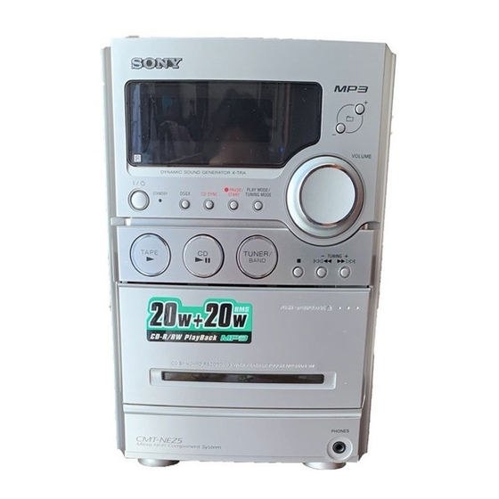
Photo: HCD-NEZ5
Model Name Using Similar Mechanism
Base Unit Name
Optical Pick-up Name
Model Name Using Similar Mechanism
Tape Transport Mechanism Type
Q Q
3
6 7
1 3
SPECIFICATIONS
20 + 20 W (6 ohms at
1 kHz, 10% THD)
1 kHz, DIN)
20 + 20 W (6 ohms at
1 kHz, 10% THD)
Sensitivity 250 mV,
impedance 47 kilohms
Accepts headphones with
an impedance of 8 ohms or
more
Accepts impedance of 6 to
16 ohms.
10 + 10 W (6 ohms at
1 kHz, 10% THD)
COMPACT DISC DECK RECEIVER
u163
.
2 9
9 4
2 8
Australian Model
Canadian Model
AEP Model
NEW
BU-K7BD81D2 or BU-K8BD83S-WOD
KSM-213EDP or KSM-213CDP
NEW
CMAL5Z231
1 5
0 5
8
2 9
9 4
European model:
DIN power output (rated): 11 + 11 W (6 ohms at
Continuous RMS power output (reference):
Music power output (reference):
Other models:
The following measured at AC 120, 220 or 240 V,
50/60 Hz
DIN power output (rated): 11 + 11 W (6 ohms at
Continuous RMS power output (reference):
Inputs
AUDIO IN:
Outputs
PHONES:
SPEAKER:
– Continued on next page –
m
co
9 9
US Model
HCD-NEZ3
UK Model
E Model
HCD-NEZ3/NEZ5
2 8
9 9
1 kHz, DIN)
15 + 15 W (6 ohms at
1 kHz, 10% THD)
28 + 28 W
1 kHz, DIN)
15 + 15 W (6 ohms at
1 kHz, 10% THD)
Sensitivity 250 mV,
impedance 47 kilohms
Accepts headphones with
an impedance of 8 ohms or
more
Accepts impedance of 6 to
16 ohms.
Advertisement
Chapters
Table of Contents

Related Manuals for Sony HCD-NEZ3


Summary of Contents for Sony HCD-NEZ3
- Page 1 Canadian Model AEP Model UK Model E Model HCD-NEZ3/NEZ5 • HCD-NEZ3 is the amplifier, CD player, tape deck and tuner section in CMT-NEZ3. • HCD-NEZ5 is the amplifier, CD player, tape deck and tuner section in CMT-NEZ5. Photo: HCD-NEZ5 Model Name Using Similar Mechanism...
- Page 2 WITH MARK 0 ON THE SCHEMATIC DIAGRAMS AND IN FONCTIONNEMENT. NE REMPLACER CES COM- POSANTS THE PARTS LIST ARE CRITICAL TO SAFE OPERATION. QUE PAR DES PIÈCES SONY DONT LES NUMÉROS SONT REPLACE THESE COMPONENTS WITH SONY PARTS WHOSE DONNÉS DANS CE MANUEL OU DANS LES SUPPLÉMENTS PART NUMBERS APPEAR AS SHOWN IN THIS MANUAL OR PUBLIÉS PAR SONY.
-
Page 3: Table Of Contents
HCD-NEZ3/NEZ5 Ver. 1.1 3 7 63 1515 0 TABLE OF CONTENTS SERVICING NOTES ..........4 GENERAL ..............6 DISASSEMBLY 3-1. Disassembly Flow ............8 3-2. Cabinet ................8 3-3. Cabinet (Top) Section ............9 3-4. Base Unit (BU-K7BD81D2) ........... 9 3-5. -
Page 4: Servicing Notes
HCD-NEZ3/NEZ5 SECTION 1 SERVICING NOTES 3 7 63 1515 0 NOTES ON LASER DIODE EMISSION CHECK NOTES ON HANDLING THE OPTICAL PICK-UP The laser beam on this model is concentrated so as to be focused on BLOCK OR BASE UNIT... - Page 5 HCD-NEZ3/NEZ5 3 7 63 1515 0 SERVICE POSITION – CD BOARD – CD board cabinet (top) section L 13942296513 – TAPE MECHANICAL DECK – u163 tape mechanical deck http://www.xiaoyu163.com...
-
Page 6: General
HCD-NEZ3/NEZ5 SECTION 2 This section is extracted from instruction manual. GENERAL 3 7 63 1515 0 Main unit BUTTON DESCRIPTIONS ALPHABETICAL ORDER ?/1 (power) 1 A – S T – Z z PAUSE/START 4 CD SYNC qk Tape deck qs... - Page 7 HCD-NEZ3/NEZ5 3 7 63 1515 0 Remote control ALPHABETICAL ORDER BUTTON DESCRIPTIONS ?/1 (power) 1 A – O P – Z m/M (rewind/fast forward) CD qh PLAY MODE qk CLEAR qd REPEAT 4 N (play) 8 CLOCK/TIMER SELECT 2 SLEEP w;...
-
Page 8: Disassembly
HCD-NEZ3/NEZ5 Ver. 1.1 SECTION 3 DISASSEMBLY 3 7 63 1515 0 • This set can be disassembled in the order shown below. 3-1. DISASSEMBLY FLOW 3-2. CABINET (Page 8) 3-3. CABINET (TOP) SECTION (Page 9) 3-5. FRONT PANEL SECTION 3-4. -
Page 9: Cabinet (Top) Section
HCD-NEZ3/NEZ5 Ver. 1.1 3 7 63 1515 0 3-3. CABINET (TOP) SECTION 6 cabinet (top) section 5 connector (S1820) 4 wire (flat type) (27 core) (CN317) 1 screw 2 claw (BVTP 2.6 × 8) 2 claw 1 screw (BVTP 2.6 × 8) L 13942296513 3-4. -
Page 10: Front Panel Section
HCD-NEZ3/NEZ5 3 7 63 1515 0 3-5. FRONT PANEL SECTION 5 connector (CN301) 4 wire (flat type) (9 core) (FFC1803) (CN900) 7 front panel section 2 wire (flat type) (13 core) (FFC1804) (except NEZ5: AEP, UK models) wire (flat type) (15 core) (FFC1804) (NEZ5: AEP, UK models) -
Page 11: Main Board
HCD-NEZ3/NEZ5 3 7 63 1515 0 3-7. MAIN BOARD 4 wire (flat type) (11 core) (except NEZ5: AEP, UK models) wire (flat type) (15 core) (NEZ5: AEP, UK models) (CN319) 2 screw (BVTP 3 × 8) 1 two connectors... -
Page 12: Test Mode
HCD-NEZ3/NEZ5 SECTION 4 TEST MODE 3 7 63 1515 0 COLD RESET CD ERROR HISTORY * The cold reset clears all data including preset data stored in * This mode can be used for CD error history display. the RAM to initial conditions. Execute this mode when Procedure: returning the set to the customer. -
Page 13: Mechanical Adjustments
HCD-NEZ3/NEZ5 SECTION 5 SECTION 6 MECHANICAL ADJUSTMENTS ELECTRICAL ADJUSTMENTS 3 7 63 1515 0 • Precaution DECK SECTION 0 dB=0.775 V 1. Clean the following parts with a denatured-alcohol-moistened swab : 1. Demagnetize the record/playback head with a head... - Page 14 HCD-NEZ3/NEZ5 3 7 63 1515 0 2. Turn the adjustment screw and check output peaks. If the peaks CD SECTION do not match for L-CH and R-CH, turn the adjustment screw so that outputs match within 1dB of peak.
-
Page 15: Diagrams
HCD-NEZ3/NEZ5 SECTION 7 3 7 6 3 1 5 1 5 0 DIAGRAMS 7-1. BLOCK DIAGRAM – CD SERVO Section – FILTER XTSL CD DSP XTAO IC101 (1/2) CLOCK X171 51 53 50 52 DETECTOR XTAI D +3.3V GENERATOR 16.9344MHz... -
Page 16: Block Diagram - Main Section
HCD-NEZ3/NEZ5 3 7 6 3 1 5 1 5 0 7-2. BLOCK DIAGRAM – MAIN Section – J321 19 AUX-L R-CH AUDIO IN OUT-L POWER J500 PHONES (Page 15) IC501 21 CD-L R-CH TUNER UNIT FM 75Ω • R-ch is omitted due to same as L-ch. - Page 17 HCD-NEZ3/NEZ5 3 7 6 3 1 5 1 5 0 • Note for Printed Wiring Boards and Schematic Diagrams • Circuit Boards Location Note on Printed Wiring Board: Note on Schematic Diagram: • X : parts extracted from the component side.
-
Page 18: Printed Wiring Board - Cd Board
HCD-NEZ3/NEZ5 3 7 6 3 1 5 1 5 0 • See page 17 for Circuit Boards Location. 7-3. PRINTED WIRING BOARD – CD Board – : Uses unleaded solder. CD BOARD (COMPONENT SIDE) M101 (SPINDLE) CD BOARD (CONDUCTOR SIDE) -
Page 19: Schematic Diagram - Cd Board
HCD-NEZ3/NEZ5 Ver. 1.1 3 7 6 3 1 5 1 5 0 7-4. SCHEMATIC DIAGRAM – CD Board – • See page 20 for Waveforms. • See page 29 for IC Block Diagrams. C131 100p TP423 IOP1 C142 1500p... - Page 20 HCD-NEZ3/NEZ5 3 7 6 3 1 5 1 5 0 • Waveforms – CD Board – – MAIN Board – – PANEL Board – IC101 yd (LRCK) T301 4 IC1801 qa (XT2) (CD PLAY mode) (REC mode) 4.4 Vp-p 81.6 Vp-p...
-
Page 21: Printed Wiring Boards - Main Section
HCD-NEZ3/NEZ5 3 7 6 3 1 5 1 5 0 • See page 17 for Circuit Boards Location. 7-5. PRINTED WIRING BOARDS – MAIN Section – : Uses unleaded solder. (Page 18) (Page 26) (NEZ5) CD BOARD DC BOARD... -
Page 22: Schematic Diagram - Main Section (1/2)
HCD-NEZ3/NEZ5 7-6. SCHEMATIC DIAGRAM – MAIN Section (1/2) – 3 7 6 3 1 5 1 5 0 (Page 23) (1/2) R236 J321 C226 R237 C227 220p 4.7k 470p FB317 AUDIO IN (EXCEPT NEZ3: US, CND, TW/NEZ5: US, CND, TW) -
Page 23: Schematic Diagram - Main Section (2/2)
HCD-NEZ3/NEZ5 3 7 6 3 1 5 1 5 0 7-7. SCHEMATIC DIAGRAM – MAIN Section (2/2) – • See page 20 for Waveforms. • See page 29 for IC Block Diagrams. (2/2) C118 R233 C218 R133 47000p 47000p ∗R531-534... -
Page 24: Printed Wiring Board - Panel Board
HCD-NEZ3/NEZ5 7-8. PRINTED WIRING BOARD – PANEL Board – • See page 17 for Circuit Boards Location. : Uses unleaded solder. 3 7 6 3 1 5 1 5 0 • Semiconductor Location Ref. No. Location MAIN BOARD MAIN BOARD... -
Page 25: Schematic Diagram - Panel Board
HCD-NEZ3/NEZ5 3 7 6 3 1 5 1 5 0 • See page 20 for Waveforms. • See page 33 for IC Pin Function Description. 7-9. SCHEMATIC DIAGRAM – PANEL Board – Q1809 LCD1801 RT1P241C-TP-1 LIQUID CRYSTAL DISPLAY C1860... -
Page 26: Printed Wiring Boards - Dc Section
HCD-NEZ3/NEZ5 7-10. PRINTED WIRING BOARDS – DC Section – • See page 17 for Circuit Boards Location. : Uses unleaded solder. 3 7 6 3 1 5 1 5 0 • Semiconductor Location Ref. No. Location (NEZ3: US, CND) -
Page 27: Printed Wiring Board - Ac Board
HCD-NEZ3/NEZ5 7-11. PRINTED WIRING BOARD – AC Board – • See page 17 for Circuit Boards Location. : Uses unleaded solder. 3 7 6 3 1 5 1 5 0 VOLTAGE NEZ3: E, E51, SP/ SELECTOR NEZ5: E, E51, SP 120Vt220Vt230 –... -
Page 28: Schematic Diagram - Power Supply Section
HCD-NEZ3/NEZ5 3 7 6 3 1 5 1 5 0 7-12. SCHEMATIC DIAGRAM – POWER SUPPLY Section – C914 D922 1SS355TE-17 ACDET ∗C921 C922 +UNREG(SUB) 1000 16V (EXCEPT NEZ3:E,E51,EA,SP/NEZ5:E,E51,SP) C930 R906 1000 35V (NEZ3:E,E51,EA,SP/NEZ5:E,E51,SP) GND(CT) C921 ∗ RELAY R911... - Page 29 HCD-NEZ3/NEZ5 3 7 63 1515 0 • IC Block Diagrams – CD Board – IC101 CXD3059AR 119 118 116 115 114 112 111 110 109 103 102 101 100 CPU INTERFACE SERVO INTERFACE 90 RMUT 89 IOVDD0 88 NC...
- Page 30 HCD-NEZ3/NEZ5 3 7 63 1515 0 IC251 BA5947FM-E2 MUTING + – INTERFACE LEVEL SHIFT INTERFACE INTERFACE VREF L 13942296513 u163 http://www.xiaoyu163.com...
- Page 31 HCD-NEZ3/NEZ5 3 7 63 1515 0 IC301 TC94A34FG-002 Timing Generator VDDP PO5/AD5 /RESET PO6/AD6 STANDBY PO7AD7 /MICS /MILP MIDIO AD10 VDDT /MICK /MIACK/ SRMSTB L 13942296513 AD16 VDDT VDDM PO8/AD11 SDO0 PO9/AD12 /CCE/ PO10/ BCKO AD13 BUCK/ PO11/ LRCKO...
- Page 32 HCD-NEZ3/NEZ5 3 7 63 1515 0 IC303 BH15FB1WG THERMAL PROTECTION OVER CURRENT PROTECTION VOLTAGE CONTROL REFERENCE BLOCK L 13942296513 – MAIN Board – IC302 BD3881FV BASS BASS VOLUME TREBLE LOGIC CONTROL VOLUME TREBLE u163 http://www.xiaoyu163.com...
- Page 33 HCD-NEZ3/NEZ5 3 7 63 1515 0 • IC PIN FUNCTION DESCRIPITION PANEL BOARD IC1801 M30620FCPFP (SYSTEM CONTROLLER) Pin No. Pin Name Description 1 to 4 Not used STBYLED LED drive signal output terminal for STANDBY indicate POWER ON Power relay drive signal output terminal "H": on...
- Page 34 HCD-NEZ3/NEZ5 3 7 63 1515 0 Pin No. Pin Name Description TAMUTE Line muting on/off control signal output terminal Not used AMPSTBY Standby control signal output to the power amplifier VDD2 Power supply terminal (+3.3V) Not used Ground terminal...
-
Page 35: Exploded Views
HCD-NEZ3/NEZ5 SECTION 8 EXPLODED VIEWS 3 7 63 1515 0 NOTE: • -XX and -X mean standardized parts, so they • Items marked “*” are not stocked since they The components identified by mark 0 or dotted line with mark 0 are may have some difference from the original are seldom required for routine service. -
Page 36: Mechanical Deck Section
HCD-NEZ3/NEZ5 3 7 63 1515 0 8-2. MECHANICAL DECK SECTION not supplied not supplied PANEL board section not supplied (WIRE200) L 13942296513 not supplied (EPT500) FFC501 HEAD PHONE board Ref. No. Part No. Description Remark Ref. No. Part No. -
Page 37: Panel Board Section
HCD-NEZ3/NEZ5 3 7 63 1515 0 8-3. PANEL BOARD SECTION FFC1803 PANEL board FFC1804 D1804, D1805 LCD1801 FFC805 FFC801 L 13942296513 Ref. No. Part No. Description Remark Ref. No. Part No. Description Remark 2-581-385-02 KNOB (VOL) (NEZ3) 2-581-391-01 PLATE, LIGHT GUIDE... -
Page 38: Cabinet (Top) Section
HCD-NEZ3/NEZ5 Ver. 1.1 3 7 63 1515 0 8-4. CABINET (TOP) SECTION S1820 (including spindle motor (M101), sled motor (M102)) L 13942296513 not supplied (sled motor (M102)) not supplied (spindle motor (M101)) S101 The components identified by Les composants identifiés par une... -
Page 39: Main Board Section
HCD-NEZ3/NEZ5 3 7 63 1515 0 8-5. MAIN BOARD SECTION (NEZ3: EXCEPT US, CND) (NEZ3: EXCEPT US, CND, MX, KR) not supplied AC board, (NEZ5: EXCEPT US, CND) MAIN board DC board section (NEZ5) not supplied (WIRE900) not supplied... -
Page 40: Ac Board, Dc Board Section
HCD-NEZ3/NEZ5 3 7 63 1515 0 8-6. AC BOARD, DC BOARD SECTION not supplied (TRANS FIXED board) DC board T902 L 13942296513 The components identified by Les composants identifiés par une mark 0 or dotted line with marque 0 sont critiques pour la mark 0 are critical for safety. - Page 41 HCD-NEZ3/NEZ5 Ver. 1.1 SECTION 9 3 7 63 1515 0 ELECTRICAL PARTS LIST NOTE: • Due to standardization, replacements in the • Items marked “*” are not stocked since they The components identified by mark 0 or dotted line with mark 0 are parts list may be different from the parts are seldom required for routine service.
- Page 42 HCD-NEZ3/NEZ5 Ver. 1.1 3 7 63 1515 0 Ref. No. Part No. Description Remark Ref. No. Part No. Description Remark C131 1-162-927-11 CERAMIC CHIP 100PF CN201 1-818-350-11 CONNECTOR (FFC) 27P C132 1-117-863-11 CERAMIC CHIP 0.47uF 6.3V C133 1-162-970-11 CERAMIC CHIP 0.01uF...
- Page 43 HCD-NEZ3/NEZ5 CONNECT HEAD PHONE 3 7 63 1515 0 Ref. No. Part No. Description Remark Ref. No. Part No. Description Remark R351 1-216-809-11 METAL CHIP 1/10W < DIODE > R352 1-216-809-11 METAL CHIP 1/10W R353 1-216-809-11 METAL CHIP 1/10W...
- Page 44 HCD-NEZ3/NEZ5 HEAD PHONE MAIN 3 7 63 1515 0 Ref. No. Part No. Description Remark Ref. No. Part No. Description Remark A-1095-970-A MAIN BOARD, COMPLETE < FLAT TYPE WIRE > (NEZ5: E, E51, SP, AR) A-1098-686-A MAIN BOARD, COMPLETE (NEZ3: MX)
- Page 45 HCD-NEZ3/NEZ5 MAIN 3 7 63 1515 0 Ref. No. Part No. Description Remark Ref. No. Part No. Description Remark C219 1-162-974-11 CERAMIC CHIP 0.01uF C370 1-164-360-11 CERAMIC CHIP 0.1uF C220 1-162-960-11 CERAMIC CHIP 220PF (NEZ3: AEP, UK, EE, RU, EA, KR, AUS/...
- Page 46 HCD-NEZ3/NEZ5 MAIN 3 7 63 1515 0 Ref. No. Part No. Description Remark Ref. No. Part No. Description Remark < IC > R118 1-216-833-11 METAL CHIP 1/10W R119 1-216-833-11 METAL CHIP 1/10W IC302 6-702-895-01 IC BD3881FV R120 1-216-833-11 METAL CHIP...
- Page 47 HCD-NEZ3/NEZ5 MAIN 3 7 63 1515 0 Ref. No. Part No. Description Remark Ref. No. Part No. Description Remark R233 1-216-864-11 SHORT CHIP R386 1-260-320-11 CARBON 1/2W R234 1-216-864-11 SHORT CHIP (EXCEPT NEZ3/NEZ5: AEP, UK, EE, RU) R235 1-216-845-11 METAL CHIP...
- Page 48 HCD-NEZ3/NEZ5 PANEL 3 7 63 1515 0 Ref. No. Part No. Description Remark Ref. No. Part No. Description Remark A-1095-891-A PANEL BOARD, COMPLETE (NEZ3: US, CND) < CONNECTOR > A-1095-895-A PANEL BOARD, COMPLETE (NEZ3: AEP, UK, EE, RU) * CN1805 1-566-970-11 HOUSING, CONNECTOR (PC BOARD) 8P...
- Page 49 HCD-NEZ3/NEZ5 PANEL 3 7 63 1515 0 Ref. No. Part No. Description Remark Ref. No. Part No. Description Remark Q1804 8-729-037-13 TRANSISTOR KTA1271Y R1820 1-216-845-11 METAL CHIP 100K 1/10W Q1805 8-729-027-43 TRANSISTOR DTC114EKA-T146 R1821 1-216-833-11 METAL CHIP 1/10W Q1806...
- Page 50 HCD-NEZ3/NEZ5 PANEL SHIELD 3 7 63 1515 0 Ref. No. Part No. Description Remark Ref. No. Part No. Description Remark 1-693-629-11 TUNER UNIT (NEZ3: AEP, UK, EE, RU, KR/ R1880 1-216-825-11 METAL CHIP 2.2K 1/10W NEZ5: KR) R1881 1-216-825-11 METAL CHIP 2.2K...
- Page 51 SUPPLEMENT-1 File this supplement with the service manual. Subject: Change of specifications Changing Destination HCD-NEZ3 : US, Canadian, AEP, UK, East European, Russian models HCD-NEZ5 : AEP, UK, East European, Russian models L 13942296513 In this set, specification have been changed in the midway of production.
-
Page 52: New/Former Type Discrimination
HCD-NEZ3/NEZ5 Ver. 1.3 3 7 63 1515 0 NEW/FORMER TYPE DISCRIMINATION New/former type can be distinguished in the version display mode of the test mode. Procedure: 1. Press the button to turn the power on. 2. While pressing the [DSGX] button, press the button and turn the [VOLUME] knob in the counter-clock wise. -
Page 53: Disassembly
HCD-NEZ3/NEZ5 3 7 63 1515 0 DISASSEMBLY • This set can be disassembled in the order shown below. 2-1. DISASSEMBLY FLOW 2-2. CABINET (Page 3) 2-3. CABINET (TOP) SECTION (Page 4 2-5. FRONT PANEL SECTION 2-4. BASE UNIT (BU-K8BD83S-WOD) - Page 54 HCD-NEZ3/NEZ5 3 7 63 1515 0 2-3. CABINET (TOP) SECTION 6 cabinet (top) section 5 connector (S1820) 4 wire (flat type) (23 core) (CN317) 1 screw 2 claw (BVTP 2.6 × 8) 2 claw 1 screw (BVTP 2.6 × 8) L 13942296513 2-4.
-
Page 55: Mechanical Deck (Cmal5Z231)
HCD-NEZ3/NEZ5 3 7 63 1515 0 2-5. FRONT PANEL SECTION 5 connector (CN301) 4 wire (flat type) (9 core) (FFC803) (CN900) 7 front panel section 2 wire (flat type) (13 core) (FFC804) (NEZ3) wire (flat type) (15 core) (FFC804) (NEZ5) -
Page 56: Main Board
HCD-NEZ3/NEZ5 3 7 63 1515 0 2-7. MAIN BOARD 4 wire (flat type) (11 core) (NEZ3) wire (flat type) (15 core) (NEZ5) (CN319) 2 screw (BVTP 3 × 8) 1 two connectors (CN314, CN318) 5 MAIN board L 13942296513 2-8. -
Page 57: Electrical Adjustments
HCD-NEZ3/NEZ5 3 7 63 1515 0 ELECTRICAL ADJUSTMENTS 2. Turn the adjustment screw and check output peaks. If the peaks do not match for L-CH and R-CH, turn the adjustment screw so that outputs match within 1dB of peak. - Page 58 HCD-NEZ3/NEZ5 3 7 63 1515 0 CD SECTION Note: 1. CD Block is basically constructed to operate without adjustment. 2. Use YEDS-18 disc (3-702-101-01) unless otherwise indicated. 3. Use an oscilloscope with more than 10 MW impedance. 4. Clean the object lens by an applicator with neutral detergent when the signal level is low than specified value with the following checks.
-
Page 59: Diagrams
HCD-NEZ3/NEZ5 DIAGRAMS 3 7 6 3 1 5 1 5 0 4-1. BLOCK DIAGRAM – CD SERVO Section – OPTICAL PICK-UP BLOCK (KSM-213CDP) RFACO RFACI AOUT1 112 (Page 10) AOUT2 117 R-CH XTAI 109 AUTOMATIC X201 POWER CONTROL 16.9344MHz... -
Page 60: Block Diagram - Main Section
HCD-NEZ3/NEZ5 3 7 6 3 1 5 1 5 0 4-2. BLOCK DIAGRAM – MAIN Section – J321 19 AUX-L R-CH AUDIO IN OUT-L POWER J500 PHONES (Page 9) IC501 21 CD-L R-CH TUNER (FM/AM) FM 75Ω • R-ch is omitted due to same as L-ch. - Page 61 HCD-NEZ3/NEZ5 3 7 6 3 1 5 1 5 0 • Note for Printed Wiring Boards and Schematic Diagrams • Circuit Boards Location Note on Printed Wiring Board: Note on Schematic Diagram: • X : parts extracted from the component side.
-
Page 62: Printed Wiring Board - Cd Board
HCD-NEZ3/NEZ5 3 7 6 3 1 5 1 5 0 • See page 11 for Circuit Boards Location. 4-3. PRINTED WIRING BOARD – CD Board – : Uses unleaded solder. M401 (SPINDLE) CD BOARD (COMPONENT SIDE) CD BOARD (CONDUCTOR SIDE) -
Page 63: Schematic Diagram - Cd Board
HCD-NEZ3/NEZ5 3 7 6 3 1 5 1 5 0 • See page 14 for Waveforms. • See page 23 for IC Block Diagrams. • See page 24 for IC Pin Function Description. 4-4. SCHEMATIC DIAGRAM – CD Board –... - Page 64 HCD-NEZ3/NEZ5 3 7 6 3 1 5 1 5 0 • Waveforms – CD Board – – MAIN Board – – PANEL Board – IC201 1 (LRCK) T301 4 IC801 qf (X1A) (CD PLAY mode) (REC mode) 3.3 Vp-p 81.6 Vp-p...
-
Page 65: Printed Wiring Boards - Main Section
HCD-NEZ3/NEZ5 3 7 6 3 1 5 1 5 0 • See page 11 for Circuit Boards Location. 4-5. PRINTED WIRING BOARDS – MAIN Section – : Uses unleaded solder. (Page 12) (Page 18) (Page 20) (NEZ5) M301 CD BOARD... -
Page 66: Schematic Diagram - Main Section (1/2)
HCD-NEZ3/NEZ5 4-6. SCHEMATIC DIAGRAM – MAIN Section (1/2) – 3 7 6 3 1 5 1 5 0 (Page 17) (1/2) R236 C309 CN317 D304 D303 FB306 1000 1N4002B 1N4002B VM(7V) J321 C226 R237 C227 FB317 220p 4.7k 470p... -
Page 67: Schematic Diagram - Main Section (2/2)
HCD-NEZ3/NEZ5 3 7 6 3 1 5 1 5 0 • See page 23 for IC Block Diagrams. 4-7. SCHEMATIC DIAGRAM – MAIN Section (2/2) – (2/2) C118 R233 C218 R133 47000p 47000p *R529-534 (NEZ3:US,CND) 220 (NEZ3:AEP,UK,EE,RU) R134 R228... -
Page 68: Printed Wiring Board - Panel Board
HCD-NEZ3/NEZ5 • See page 11 for Circuit Boards Location. 4-8. PRINTED WIRING BOARD – PANEL Board – : Uses unleaded solder. 3 7 6 3 1 5 1 5 0 • Semiconductor Location (Page 15) Ref. No. Location MAIN BOARD... -
Page 69: Schematic Diagram - Panel Board
HCD-NEZ3/NEZ5 3 7 6 3 1 5 1 5 0 • See page 14 for Waveforms. • See page 24 for IC Pin Function Description. 4-9. SCHEMATIC DIAGRAM – PANEL Board – LCD801 LIQUID CRYSTAL DISPLAY D804,805 (LCD BACK LIGHT) -
Page 70: Printed Wiring Boards - Dc Section
HCD-NEZ3/NEZ5 • See page 11 for Circuit Boards Location. 4-10. PRINTED WIRING BOARDS – DC Section – : Uses unleaded solder. 3 7 6 3 1 5 1 5 0 • Semiconductor Location (NEZ3: US, CND) (NEZ3: AEP, UK/NEZ5) Ref. -
Page 71: Printed Wiring Board - Ac Board
HCD-NEZ3/NEZ5 • See page 11 for Circuit Boards Location. 4-11. PRINTED WIRING BOARD – AC Board – : Uses unleaded solder. 3 7 6 3 1 5 1 5 0 AC BOARD • Semiconductor Location Ref. No. Location D906... -
Page 72: Schematic Diagram - Power Supply Section
HCD-NEZ3/NEZ5 3 7 6 3 1 5 1 5 0 4-12. SCHEMATIC DIAGRAM – POWER SUPPLY Section – C914 D922 1SS355TE-17 ACDET C922 +UNREG(SUB) C930 R906 GND(CT) C921 1000 RELAY R911 D910 D909 1N4002B 1N4002B R904 +4V REGULATOR IC903 4.7k... - Page 73 HCD-NEZ3/NEZ5 3 7 63 1515 0 • IC Block Diagrams – CD Board – IC402 BA5947FM-E2 MUTING + – INTERFACE LEVEL SHIFT INTERFACE INTERFACE VREF L 13942296513 – MAIN Board – IC301 BD3881FV BASS BASS VOLUME TREBLE LOGIC CONTROL...
- Page 74 HCD-NEZ3/NEZ5 3 7 63 1515 0 • IC PIN FUNCTION DESCRIPITION CD BOARD IC201 CXD3014A-201R (CD DSP) Pin No. Pin Name Description LRCK L/R sampling clock signal output terminal LRCKI L/R sampling clock signal input terminal PCMD Serial data output terminal...
- Page 75 HCD-NEZ3/NEZ5 3 7 63 1515 0 Pin No. Pin Name Description AVDD0 Power supply terminal (+3.3V) AVSS0 Ground terminal E signal input from the optical pick-up block F signal input from the optical pick-up block Tracking error signal input terminal...
- Page 76 HCD-NEZ3/NEZ5 3 7 63 1515 0 Pin No. Pin Name Description TRST Not used Ground terminal Power supply terminal (+1.8V) IOVDD2 Power supply terminal (+3.3V) DOUT Digital audio signal output terminal Not used TEST Test terminal Normally: fixed at "L"...
- Page 77 HCD-NEZ3/NEZ5 3 7 63 1515 0 PANEL BOARD IC801 MB90803-104 (SYSTEM CONTROLLER) Pin No. Pin Name Description SEG32 Segment drive signal output to the liquid crystal display O-AMPICSTBY Standby control signal output to the power amplifier O-CD-XRST System reset signal output to the CD DSP...
- Page 78 HCD-NEZ3/NEZ5 3 7 63 1515 0 Pin No. Pin Name Description O-POWER Power relay drive signal output terminal "H": on I-SUFFIX Model destination setting terminal I-RE-VOL Dial pulse input of the rotary encoder (for VOLUME control) I-MP3-REQ MP3 data request signal input from the CD DSP...
-
Page 79: Exploded View
HCD-NEZ3/NEZ5 3 7 63 1515 0 EXPLODED VIEW NOTE: • -XX and -X mean standardized parts, so they • Items marked “*” are not stocked since they The components identified by mark 0 or dotted line with mark 0 are may have some difference from the original are seldom required for routine service. -
Page 80: Mechanical Deck Section
HCD-NEZ3/NEZ5 3 7 63 1515 0 5-2. MECHANICAL DECK SECTION not supplied not supplied PANEL board section not supplied (WIRE200) L 13942296513 not supplied (EPT500) FFC501 HEAD PHONE board Ref. No. Part No. Description Remark Ref. No. Part No. -
Page 81: Panel Board Section
HCD-NEZ3/NEZ5 3 7 63 1515 0 5-3. PANEL BOARD SECTION FFC803 PANEL board FFC804 D804, D805 LCD801 FFC805 FFC801 L 13942296513 Ref. No. Part No. Description Remark Ref. No. Part No. Description Remark 2-581-385-02 KNOB (VOL) (NEZ3) D804 6-501-138-01 DIODE SELU2WA10C-LF62 (LCD BACK LIGHT) -
Page 82: Cabinet (Top) Section
HCD-NEZ3/NEZ5 3 7 63 1515 0 5-4. CABINET (TOP) SECTION S820 (including spindle motor (M401), L 13942296513 sled motor (M402)) included in (sled motor (M402)) included in (spindle motor (M401)) S201 Ref. No. Part No. Description Remark Ref. No. -
Page 83: Main Board Section
HCD-NEZ3/NEZ5 3 7 63 1515 0 5-5. MAIN BOARD SECTION AC board, MAIN board DC board section (NEZ5) not supplied (WIRE900) not supplied (NEZ3: US, CND) L 13942296513 (NEZ3: AEP, UK, EE, RU/NEZ5) not supplied not supplied Ref. No. -
Page 84: Ac Board, Dc Board Section
HCD-NEZ3/NEZ5 3 7 63 1515 0 5-6. AC BOARD, DC BOARD SECTION not supplied (TRANS FIXED board) DC board T902 L 13942296513 Ref. No. Part No. Description Remark Ref. No. Part No. Description Remark A-1139-348-A DC BOARD, COMPLETE 2-594-960-11 SPACER (TRANSFORMER) -
Page 85: Electrical Parts List
HCD-NEZ3/NEZ5 3 7 63 1515 0 ELECTRICAL PARTS LIST NOTE: • Due to standardization, replacements in the • Items marked “*” are not stocked since they The components identified by mark are seldom required for routine service. 0 or dotted line with mark 0 are... - Page 86 HCD-NEZ3/NEZ5 CONNECT 3 7 63 1515 0 Ref. No. Part No. Description Remark Ref. No. Part No. Description Remark R113 1-216-809-11 METAL CHIP 1/10W C256 1-107-826-11 CERAMIC CHIP 0.1uF R201 1-216-295-00 SHORT CHIP C257 1-107-826-11 CERAMIC CHIP 0.1uF R202...
- Page 87 HCD-NEZ3/NEZ5 HEAD PHONE 3 7 63 1515 0 Ref. No. Part No. Description Remark Ref. No. Part No. Description Remark C918 1-104-655-91 ELECT 470uF 6.3V A-1139-347-A HEAD PHONE BOARD, COMPLETE (NEZ3: US, CND) C919 1-126-943-21 ELECT 2200uF A-1139-427-A HEAD PHONE BOARD, COMPLETE (NEZ5)
- Page 88 HCD-NEZ3/NEZ5 MAIN 3 7 63 1515 0 Ref. No. Part No. Description Remark Ref. No. Part No. Description Remark C236 1-126-964-11 ELECT 10uF A-1139-350-A MAIN BOARD, COMPLETE (NEZ3: US, CND) C238 1-126-965-11 ELECT 22uF A-1139-421-A MAIN BOARD, COMPLETE (NEZ5)
- Page 89 HCD-NEZ3/NEZ5 MAIN 3 7 63 1515 0 Ref. No. Part No. Description Remark Ref. No. Part No. Description Remark C513 1-126-957-11 ELECT 0.22uF Q328 8-729-120-28 TRANSISTOR 2SC1623-L5L6 C514 1-136-169-00 FILM 0.22uF Q329 8-729-120-28 TRANSISTOR 2SC1623-L5L6 C516 1-126-933-11 ELECT 100uF...
- Page 90 HCD-NEZ3/NEZ5 MAIN 3 7 63 1515 0 Ref. No. Part No. Description Remark Ref. No. Part No. Description Remark R203 1-216-817-11 METAL CHIP 1/10W R319 1-216-837-11 METAL CHIP 1/10W R204 1-216-805-11 METAL CHIP 1/10W R328 1-216-833-11 METAL CHIP 1/10W...
- Page 91 HCD-NEZ3/NEZ5 MAIN PANEL 3 7 63 1515 0 Ref. No. Part No. Description Remark Ref. No. Part No. Description Remark R523 1-216-864-11 SHORT CHIP 0 (NEZ5) D804 6-501-138-01 LED SELU2WA10C-LF62 (LCD BACK LIGHT) R524 1-216-809-11 METAL CHIP 1/10W (NEZ5)
- Page 92 HCD-NEZ3/NEZ5 PANEL 3 7 63 1515 0 Ref. No. Part No. Description Remark Ref. No. Part No. Description Remark R708 1-216-825-11 METAL CHIP 2.2K 1/10W R850 1-216-821-11 METAL CHIP 1/10W (NEZ3: AEP, UK, EE, RU/NEZ5) R851 1-216-825-11 METAL CHIP 2.2K...
- Page 93 HCD-NEZ3/NEZ5 PANEL SHIELD 3 7 63 1515 0 Ref. No. Part No. Description Remark Ref. No. Part No. Description Remark X802 1-795-054-61 VIBRATOR, CERAMIC (10MHz) ************************************************************ A-1139-356-A SHIELD BOARD, COMPLETE (NEZ3: US, CND) *********************** ************************************************************ MISCELLANEOUS ************** 1-796-352-71 DECK, MECHANICAL (CMAL5Z231)
- Page 94 HCD-NEZ3/NEZ5 3 7 63 1515 0 REVISION HISTORY Clicking the version allows you to jump to the revised page. Also, clicking the version at the upper right on the revised page allows you to jump to the next revised page.
Need help?
Do you have a question about the HCD-NEZ3 and is the answer not in the manual?
Questions and answers
What's the number of speaker output ic or power amplifier
The speaker output IC or power amplifier number for the Sony HCD-NEZ3 is IC501, which is the LM1876TF.
This answer is automatically generated
What's the ic number of speaker output
The IC number for the speaker output of the Sony HCD-NEZ3 is IC501 (LM1876TF).
This answer is automatically generated
Number of output ic
Based on the provided context, there is one output IC mentioned: IC251 (BA5947FM-E2), which is related to motor/coil drive and output functions such as CH4OUTF, CH4OUTR, and OPOUT. Therefore, the Sony HCD-NEZ3 has 1 output IC.
This answer is automatically generated