Table of Contents
Advertisement
QQ
3 7 63 1515 0
SERVICE MANUAL
Ver. 1.5 2007.04
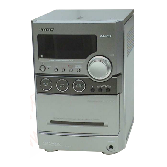
• HCD-NEZ30 is the amplifier, CD player, tape deck
and tuner section in CMT-NEZ30.
TE
L 13942296513
AUDIO POWER SPECIFICATIONS
POWER OUTPUT AND TOTAL HARMONIC DISTORTION:
( The United States model only)
With 6 ohm loads, both channels driven, from 120 – 10,000 Hz; rated 15 watts
per channel minimum RMS power, with no more than 10% total harmonic
distortion from 250 milliwatts to rated output.
Amplifier section
North-American model:
Continuous RMS power output (reference): 15 + 15 W (6 ohms at 1 kHz,
10% THD)
European model:
DIN power output (rated): 11 + 11 W (6 ohms at 1 kHz, DIN)
Continuous RMS power output (reference): 17 + 17 W (6 ohms at 1 kHz,
10% THD)
Music power output (reference): 28 + 28 W
The following are measured at AC 220 V, 50/60 Hz (Argentine model), AC
120 V, 60 Hz (Mexican model), AC 120, 220 or 230 – 240 V, 50/60 Hz (other
models)
DIN power output (rated): 11 + 11 W (6 ohms at 1 kHz, DIN)
Continuous RMS power output (reference): 15 + 15 W (6 ohms at 1 kHz,
10% THD)
Inputs
AUDIO IN: Sensitivity 250 mV, impedance 47 kilohms
Outputs
PHONES: Accepts headphones with an impedance of 8 ohms or more
SPEAKER: Accepts impedance of 6 to 16 ohms
CD player section
System: Compact disc and digital audio system
Laser Diode Properties
Emission Duration: Continuous
Laser Output*: Less than 44.6µW
* This output is the value measurement at a distance of 200 mm from the
objective lens surface on the Optical Pick-up Block with 7mm aperture.
Tape deck section
Recording system: 4-track 2-channel, stereo
Tuner section
FM stereo, FM/AM superheterodyne tuner
www
.
Sony Corporation
9-887-030-06
Personal Audio Division
2007D05-1
Published by Sony Techno Create Corporation
© 2007.04
http://www.xiaoyu163.com
CD Section
TAPE Section
x
ao
u163
y
i
http://www.xiaoyu163.com
HCD-NEZ30
2 9
8
Model Name Using Similar Mechanism
Base Unit Name
Optical Pick-up block Name
Model Name Using Similar Mechanism
Tape Transport Mechanism Type
Q Q
3
6 7
1 3
1 5
SPECIFICATIONS
FM tuner section:
Tuning range
North American model: 87.5 – 108.0 MHz (100 kHz step)
Other models: 87.5 – 108.0 MHz (50 kHz step)
Antenna: FM lead antenna
Antenna terminals: 75 ohms unbalanced
Intermediate frequency: 10.7 MHz
AM tuner section:
Tuning range
Pan-American model: 530 – 1,710 kHz (with 10 kHz tuning interval)
European models: 531 – 1,602 kHz (with 9 kHz tuning interval)
Other models: 530 – 1,710 kHz (with 10 kHz tuning interval)
531 – 1,602 kHz (with 9 kHz tuning interval)
Antenna: AM loop antenna, external antenna terminal
Intermediate frequency: 450 kHz
General
Power requirements
North American model: AC 120 V, 60 Hz
Mexican model: AC 120 V, 60 Hz
European model: AC 230 V, 50/60 Hz
Argentine model: AC 220 V, 50/60 Hz
Other models: AC 120, 220 or 230 – 240 V, 50/60 Hz
Adjustable with voltage selector
Power consumption:
North American model: 45 watts
Other models: 45 watts
Dimensions (w/h/d) (excl. speakers):
Approx. 164 × 235 × 265 mm
Mass (excl. speakers):
North
American model: Approx. 3.2 kg
European model: Approx. 3.6 kg
Other models: Approx. 3.3 kg
Design and specifications are subject to change without notice.
COMPACT DISC DECK RECEIVER
co
.
9 4
2 8
US Model
Canadian Model
UK Model
East European Model
HCD-NEZ3
BU-K8BD83S-WOD
KSM-213CDP
NEW
CMAL5Z235A
0 5
8
2 9
9 4
2 8
531 – 1,710 kHz (with 9 kHz tuning interval)
m
9 9
E Model
9 9
Advertisement
Table of Contents

Related Manuals for Sony HCD-NEZ30


Summary of Contents for Sony HCD-NEZ30
-
Page 1: Specifications
US Model Canadian Model Ver. 1.5 2007.04 UK Model E Model East European Model • HCD-NEZ30 is the amplifier, CD player, tape deck and tuner section in CMT-NEZ30. Model Name Using Similar Mechanism HCD-NEZ3 CD Section Base Unit Name BU-K8BD83S-WOD... - Page 2 WITH MARK 0 ON THE SCHEMATIC DIAGRAMS AND IN FONCTIONNEMENT. NE REMPLACER CES COM- POSANTS THE PARTS LIST ARE CRITICAL TO SAFE OPERATION. QUE PAR DES PIÈCES SONY DONT LES NUMÉROS SONT REPLACE THESE COMPONENTS WITH SONY PARTS WHOSE DONNÉS DANS CE MANUEL OU DANS LES SUPPLÉMENTS PART NUMBERS APPEAR AS SHOWN IN THIS MANUAL OR PUBLIÉS PAR SONY.
-
Page 3: Table Of Contents
HCD-NEZ30 Ver. 1.5 SECTION 1 SERVICING NOTES 3 7 63 1515 0 TABLE OF CONTENTS NOTES ON HANDLING THE OPTICAL PICK-UP BLOCK OR BASE UNIT SERVICING NOTES ..........3 The laser diode in the optical pick-up block may suffer electrostatic... - Page 4 HCD-NEZ30 Ver. 1.5 3 7 63 1515 0 LASER DIODE AND FOCUS SEARCH OPERATION NOTE WHEN PARTS RELATED TO POWER CHECK TRANSFORMER ARE REPLACED During normal operation of the equipment, emission of the laser In this set, the main power transformer (T902) and sub power...
- Page 5 HCD-NEZ30 3 7 63 1515 0 SERVICE POSITION – CD BOARD – CD board cabinet (top) section L 13942296513 – TAPE MECHANICAL DECK – u163 tape mechanical deck http://www.xiaoyu163.com...
-
Page 6: General
HCD-NEZ30 Ver. 1.1 SECTION 2 This section is extracted from instruction manual. GENERAL 3 7 63 1515 0 Basic Operations To stop automatic scanning Set the sound effect on the remote Press (stop) repeatedly to select “BASS” or “TREBLE,” and then... -
Page 7: Other Operations
HCD-NEZ30 Ver. 1.1 3 7 63 1515 0 Other Operations Select the sound source or prepare the tape. Creating your own CD program Recording onto a tape For Play Timer: (Program Play) You can record on a TYPE I (normal) tape in two ways:... -
Page 8: Disassembly
HCD-NEZ30 SECTION 3 DISASSEMBLY 3 7 63 1515 0 • This set can be disassembled in the order shown below. 3-1. DISASSEMBLY FLOW 3-2. CABINET (Page 8) 3-3. CABINET (TOP) SECTION (Page 9) 3-5. FRONT PANEL SECTION 3-4. BASE UNIT (BU-K8BD83S-WOD) -
Page 9: Cabinet (Top) Section
HCD-NEZ30 3 7 63 1515 0 3-3. CABINET (TOP) SECTION 6 cabinet (top) section 5 connector (S820) 4 wire (flat type) (23 core) (CN317) 1 screw 2 claw (BVTP 2.6) 2 claw 1 screw (BVTP 2.6) L 13942296513 3-4. BASE UNIT (BU-K8BD83S-WOD) -
Page 10: Front Panel Section
HCD-NEZ30 3 7 63 1515 0 3-5. FRONT PANEL SECTION 5 connector (CN301) 4 flexible flat cable (9 core) (FFC803) (CN900) 9 front panel section 2 flexible flat cable (11 core) (FFC804) (CN320) 3 flexible flat cable (17 core) (FFC805) -
Page 11: Main Board
HCD-NEZ30 Ver. 1.5 3 7 63 1515 0 3-7. MAIN BOARD 2 screw (BVTT 3 × 8) 9 heat sink 4 flexible flat cable (9 core) (CN319) 0 Remove two solders. 1 two connectors 6 screw (CN902, CN903) 8 IC bracket (BVTP 3 ×... -
Page 12: Test Mode
HCD-NEZ30 Ver. 1.5 SECTION 4 TEST MODE 3 7 63 1515 0 COLD RESET CD ERROR HISTORY The cold reset clears all data including preset data stored in the When this mode is entered, optical pick-up error code is displayed RAM to initial conditions. -
Page 13: Mechanical Adjustments
HCD-NEZ30 SECTION 5 3 7 63 1515 0 MECHANICAL ADJUSTMENTS • Precaution CD POWER MANEGE This mode is for switch the CD power supply on/off. Even if this 1. Clean the following parts with a denatured-alcohol-moistened state pulls out AC plug, it is held. -
Page 14: Electrical Adjustments
HCD-NEZ30 SECTION 6 ELECTRICAL ADJUSTMENTS 3 7 63 1515 0 2. Turn the adjustment screw and check output peaks. If the peaks DECK SECTION 0 dB=0.775 V do not match for L-CH and R-CH, turn the adjustment screw so that outputs match within 1dB of peak. - Page 15 HCD-NEZ30 3 7 63 1515 0 CD SECTION Note: 1. CD Block is basically constructed to operate without adjustment. 2. Use YEDS-18 disc (3-702-101-01) unless otherwise indicated. 3. Use an oscilloscope with more than 10 MΩ impedance. 4. Clean the object lens by an applicator with neutral detergent when the signal level is low than specified value with the following checks.
- Page 16 HCD-NEZ30 3 7 63 1515 0 MEMO L 13942296513 u163 http://www.xiaoyu163.com...
-
Page 17: Diagrams
HCD-NEZ30 SECTION 7 3 7 6 3 1 5 1 5 0 DIAGRAMS 7-1. BLOCK DIAGRAM – CD SERVO Section – OPTICAL PICK-UP BLOCK (KSM-213CDP) RFACO RFACI AOUT1 112 AOUT2 117 R-CH (Page 18) XTAI 109 AUTOMATIC X201 POWER CONTROL 16.9344MHz... -
Page 18: Block Diagram - Main Section
HCD-NEZ30 Ver. 1.1 3 7 6 3 1 5 1 5 0 7-2. BLOCK DIAGRAM – MAIN Section – J321 19 AUX-L R-CH AUDIO IN OUT-L POWER J500 PHONES IC501 21 CD-L R-CH (Page 17) TUNER (FM/AM) FM 75Ω... - Page 19 HCD-NEZ30 Ver. 1.5 3 7 6 3 1 5 1 5 0 • Note for Printed Wiring Boards and Schematic Diagrams • Circuit Boards Location Note on Printed Wiring Board: Note on Schematic Diagram: • X : parts extracted from the component side.
-
Page 20: Printed Wiring Board - Cd Board
HCD-NEZ30 Ver. 1.5 3 7 6 3 1 5 1 5 0 • See page 19 for Circuit Boards Location. 7-3. PRINTED WIRING BOARD – CD Board – : Uses unleaded solder. M401 (SPINDLE) CD BOARD (COMPONENT SIDE) CD BOARD... -
Page 21: Schematic Diagram - Cd Board
HCD-NEZ30 Ver. 1.5 3 7 6 3 1 5 1 5 0 • See page 25 for Waveforms. • See page 25 for IC Block Diagrams. • See page 31 for IC Pin Function Description. 7-4. SCHEMATIC DIAGRAM – CD Board –... -
Page 22: Printed Wiring Boards - Main Section
HCD-NEZ30 Ver. 1.5 • See page 19 for Circuit Boards Location. 7-5. PRINTED WIRING BOARDS – MAIN Section – : Uses unleaded solder. 3 7 6 3 1 5 1 5 0 (Page 26) (Page 20) (Page 28) PANEL... -
Page 23: Schematic Diagram - Main Section (1/2)
HCD-NEZ30 Ver. 1.1 7-6. SCHEMATIC DIAGRAM – MAIN Section (1/2) – 3 7 6 3 1 5 1 5 0 (Page 24) (1/2) R236 C309 CN317 D304 D303 FB306 1000 1N4002B 1N4002B VM(7V) J321 C226 R237 C227 FB317 220p 4.7k... -
Page 24: Schematic Diagram - Main Section (2/2)
HCD-NEZ30 Ver. 1.5 3 7 6 3 1 5 1 5 0 7-7. SCHEMATIC DIAGRAM – MAIN Section (2/2) – • See page 25 for Waveforms. • See page 25 for IC Block Diagrams. (2/2) R135 R235 C218 100k... - Page 25 HCD-NEZ30 3 7 6 3 1 5 1 5 0 • Waveforms • IC Block Diagrams – CD Board – – MAIN Board – – PANEL Board – – CD Board – IC402 BA5947FM-E2 IC201 1 (LRCK) T301 4...
-
Page 26: Printed Wiring Board - Panel Board
HCD-NEZ30 Ver. 1.5 • See page 19 for Circuit Boards Location. 7-8. PRINTED WIRING BOARD – PANEL Board – : Uses unleaded solder. 3 7 6 3 1 5 1 5 0 • Semiconductor Location (Page 22) (Page 22) Ref. -
Page 27: Schematic Diagram - Panel Board
HCD-NEZ30 Ver. 1.5 3 7 6 3 1 5 1 5 0 • See page 25 for Waveforms. • See page 31 for IC Pin Function Description. 7-9. SCHEMATIC DIAGRAM – PANEL Board – LCD801 LIQUID CRYSTAL DISPLAY D804,805... -
Page 28: Printed Wiring Boards - Dc Section
HCD-NEZ30 Ver. 1.4 • See page 19 for Circuit Boards Location. 7-10. PRINTED WIRING BOARDS – DC Section – : Uses unleaded solder. 3 7 6 3 1 5 1 5 0 • Semiconductor (EXCEPT US, CND) (US, CND) -
Page 29: Printed Wiring Board - Ac Board
HCD-NEZ30 Ver. 1.5 • See page 19 for Circuit Boards Location. 7-11. PRINTED WIRING BOARD – AC Board – : Uses unleaded solder. 3 7 6 3 1 5 1 5 0 AC BOARD S901 VOLTAGE SELECTOR 230 – 240V t 220V t120V... -
Page 30: Schematic Diagram - Power Supply Section
HCD-NEZ30 Ver. 1.5 3 7 6 3 1 5 1 5 0 7-12. SCHEMATIC DIAGRAM – POWER SUPPLY Section – C914 D922 1SS355WTE-17 ACDET C922 +UNREG(SUB) C930 R906 GND(CT) C921 1000 RELAY ∗ R911 R911 D910 D909 ∗ 47k (TYPE A) (US, CND, E, E51, MX, AR) - Page 31 HCD-NEZ30 3 7 63 1515 0 • IC PIN FUNCTION DESCRIPITION CD BOARD IC201 CXD3014A-201R (CD DSP) Pin No. Pin Name Description LRCK L/R sampling clock signal output terminal LRCKI L/R sampling clock signal input terminal PCMD Serial data output terminal...
- Page 32 HCD-NEZ30 3 7 63 1515 0 Pin No. Pin Name Description AVDD0 Power supply terminal (+3.3V) AVSS0 Ground terminal E signal input from the optical pick-up block F signal input from the optical pick-up block Tracking error signal input terminal...
- Page 33 HCD-NEZ30 3 7 63 1515 0 Pin No. Pin Name Description TRST Not used Ground terminal Power supply terminal (+1.8V) IOVDD2 Power supply terminal (+3.3V) DOUT Digital audio signal output terminal Not used TEST Test terminal Normally: fixed at "L"...
- Page 34 HCD-NEZ30 Ver. 1.2 3 7 63 1515 0 PANEL BOARD IC801 MB90803PF-G-115E1 (SYSTEM CONTROLLER) Pin No. Pin Name Description SEG32 Segment drive signal output to the liquid crystal display STK-ON Standby control signal output to the power amplifier O-CD-XRST...
- Page 35 HCD-NEZ30 3 7 63 1515 0 Pin No. Pin Name Description O-POWER Power relay drive signal output terminal "H": on I-SUFFIX Model destination setting terminal I-RE-VOL Dial pulse input of the rotary encoder (for VOLUME control) I-MP3-REQ MP3 data request signal input from the CD DSP...
-
Page 36: Exploded Views
HCD-NEZ30 Ver. 1.5 SECTION 8 EXPLODED VIEWS 3 7 63 1515 0 NOTE: • -XX and -X mean standardized parts, so they • Items marked “*” are not stocked since they The components identified by mark 0 or dotted line with mark 0 are may have some difference from the original are seldom required for routine service. -
Page 37: Mechanical Deck Section
HCD-NEZ30 Ver. 1.5 3 7 63 1515 0 8-2. MECHANICAL DECK SECTION not supplied not supplied not supplied PANEL board section not supplied (WIRE200) L 13942296513 not supplied (EPT500) FFC501 HEAD PHONE board Ref. No. Part No. Description Remark Ref. -
Page 38: Panel Board Section
HCD-NEZ30 Ver. 1.5 3 7 63 1515 0 8-3. PANEL BOARD SECTION FFC803 PANEL board FFC804 D804, D805 LCD801 FFC805 FFC801 L 13942296513 Ref. No. Part No. Description Remark Ref. No. Part No. Description Remark 2-581-385-21 KNOB (VOL) 2-591-582-02 PLATE (FRONT FFC), PROTECTION... -
Page 39: Cabinet (Top) Section
HCD-NEZ30 Ver. 1.1 3 7 63 1515 0 8-4. CABINET (TOP) SECTION not supplied S820 (including spindle motor (M401), sled motor (M402)) L 13942296513 included in (sled motor (M402)) included in (spindle motor (M401)) S201 Ref. No. Part No. -
Page 40: Main Board Section
HCD-NEZ30 Ver. 1.5 3 7 63 1515 0 8-5. MAIN BOARD SECTION not supplied MAIN board AC board, DC board section not supplied (WIRE900) (US, CND) not supplied not supplied L 13942296513 (SHIELD board) (EXCEPT UK, EE) (UK, EE) not supplied Ref. -
Page 41: Ac Board, Dc Board Section
HCD-NEZ30 Ver. 1.5 3 7 63 1515 0 8-6. AC BOARD, DC BOARD SECTION not supplied (CONNECT board) DC board L 13942296513 T902 Note: Refer to “NOTE WHEN PARTS RELATED TO POWER TRANSFORMER ARE REPLACED” (page 4) in the servic- ing notes when the complete DC board or T902 is replaced. -
Page 42: Electrical Parts List
HCD-NEZ30 Ver. 1.5 SECTION 9 3 7 63 1515 0 ELECTRICAL PARTS LIST NOTE: • Due to standardization, replacements in the • Items marked “*” are not stocked since they The components identified by mark 0 or dotted line with mark 0 are parts list may be different from the parts are seldom required for routine service. - Page 43 HCD-NEZ30 CONNECT 3 7 63 1515 0 Ref. No. Part No. Description Remark Ref. No. Part No. Description Remark C224 1-164-360-11 CERAMIC CHIP 0.1uF R104 1-216-809-11 METAL CHIP 1/10W C226 1-165-908-11 CERAMIC CHIP R105 1-216-809-11 METAL CHIP 1/10W C227...
- Page 44 HCD-NEZ30 Ver. 1.5 HEAD PHONE 3 7 63 1515 0 Ref. No. Part No. Description Remark Ref. No. Part No. Description Remark A-1158-136-A DC BOARD, COMPLETE (TYPE A) R902 1-216-837-11 METAL CHIP 1/10W (US, CND, E, E51, MX, AR)
- Page 45 HCD-NEZ30 MAIN 3 7 63 1515 0 Ref. No. Part No. Description Remark Ref. No. Part No. Description Remark A-1158-128-A MAIN BOARD, COMPLETE C303 1-130-479-00 MYLAR 0.0047uF 5% ********************* C304 1-130-479-00 MYLAR 0.0047uF 5% C305 1-126-934-11 ELECT 220uF 2-586-961-01 HEAT SINK...
- Page 46 HCD-NEZ30 MAIN 3 7 63 1515 0 Ref. No. Part No. Description Remark Ref. No. Part No. Description Remark C524 1-162-915-11 CERAMIC CHIP 10PF 0.5PF < COIL > C525 1-162-966-11 CERAMIC CHIP 0.0022uF 10% L101 1-422-009-13 COIL, AIR-CORE C526 1-162-966-11 CERAMIC CHIP 0.0022uF 10%...
- Page 47 HCD-NEZ30 Ver. 1.1 MAIN 3 7 63 1515 0 Ref. No. Part No. Description Remark Ref. No. Part No. Description Remark R138 1-216-825-11 METAL CHIP 2.2K 1/10W R308 1-216-821-11 METAL CHIP 1/10W R139 1-216-837-11 METAL CHIP 1/10W R309 1-216-821-11 METAL CHIP...
- Page 48 HCD-NEZ30 Ver. 1.5 MAIN PANEL 3 7 63 1515 0 Ref. No. Part No. Description Remark Ref. No. Part No. Description Remark R523 1-216-809-11 METAL CHIP 1/10W < FLAT TYPE WIRE > R524 1-216-809-11 METAL CHIP 1/10W R535 1-260-087-11 CARBON...
- Page 49 HCD-NEZ30 Ver. 1.1 PANEL 3 7 63 1515 0 Ref. No. Part No. Description Remark Ref. No. Part No. Description Remark R716 1-216-809-11 METAL CHIP 1/10W R853 1-216-825-11 METAL CHIP 2.2K 1/10W R717 1-216-809-11 METAL CHIP 1/10W R718 1-216-809-11 METAL CHIP...
- Page 50 HCD-NEZ30 Ver. 1.5 SHIELD 3 7 63 1515 0 Ref. No. Part No. Description Remark Ref. No. Part No. Description Remark SHIELD BOARD (EXCEPT UK, EE) ************* ************************************************************ MISCELLANEOUS ************** 1-797-510-11 DECK, MECHANICAL (CMAL5Z235A) 1-452-899-11 MAGNET 0 160 8-820-126-02 OPTICAL PICK-UP BLOCK(KSM-213CDP/C2NP)
- Page 51 HCD-NEZ30 HCD-NEZ30 3 7 6 3 1 5 1 5 0 DIAGRAMS • Note for Printed Wiring Boards and Schematic Diagrams Note on Schematic Diagram: US Model Note on Printed Wiring Board: • All capacitors are in µF unless otherwise noted. (p: pF) •...
- Page 52 HCD-NEZ30 3 7 6 3 1 5 1 5 0 2-1. PRINTED WIRING BOARD – CD Board – : Uses unleaded solder. CD BOARD (COMPONENT SIDE) CD BOARD M401 (SPINDLE) (CONDUCTOR SIDE) S201 (LIMIT) C403 R280 C405 C406 IC402...
- Page 53 HCD-NEZ30 Ver. 1.4 3 7 6 3 1 5 1 5 0 2-2. SCHEMATIC DIAGRAM – CD Board – C210 C208 (RFACI) C230 R256 100p C257 C274 CN301 R266 R321 C303 C304 C301 C323 C322 R324 100k R267 R257 R322 4.7k...
- Page 54 HCD-NEZ30 Ver. 1.5 3 7 6 3 1 5 1 5 0 2-3. SCHEMATIC DIAGRAM – MAIN Board (1/2) – (Page 5) (1/2) R236 C309 CN317 D304 D303 FB306 1000 1N4002B 1N4002B VM(7V) J321 C226 R237 C227 FB317 (EXCEPT UK, EE) 220p 4.7k...
- Page 55 HCD-NEZ30 Ver. 1.5 3 7 6 3 1 5 1 5 0 2-4. SCHEMATIC DIAGRAM – MAIN Board (2/2) – (2/2) R135 R235 C218 100k 100k 47000p C118 R233 R234 R133 47000p R134 C235 R228 R231 R128 R232 R131...
- Page 56 HCD-NEZ30 Ver. 1.5 3 7 6 3 1 5 1 5 0 2-5. PRINTED WIRING BOARD – MAIN Board – : Uses unleaded solder. PANEL CD BOARD DC BOARD TO SHIELD BOARD BOARD CN102 CN903 MAIN BOARD C354 Q344...
- Page 57 HCD-NEZ30 Ver. 1.5 SECTION 3 3 7 63 1515 0 ELECTRICAL PARTS LIST NOTE: • Due to standardization, replacements in the • Items marked “*” are not stocked since they The components identified by mark 0 or dotted line with mark 0 are parts list may be different from the parts are seldom required for routine service.
- Page 58 HCD-NEZ30 Ver. 1.5 MAIN 3 7 63 1515 0 Ref. No. Part No. Description Remark Ref. No. Part No. Description Remark < TRANSISTOR > A-1158-128-A MAIN BOARD, COMPLETE (US, CND) A-1158-557-A MAIN BOARD, COMPLETE (E, E51, MX, AR) Q321...
- Page 59 HCD-NEZ30 Ver. 1.5 MAIN 3 7 63 1515 0 Ref. No. Part No. Description Remark Ref. No. Part No. Description Remark C239 1-162-962-11 CERAMIC CHIP 470PF C361 1-126-947-11 ELECT 47uF C240 1-162-960-11 CERAMIC CHIP 220PF (US, CND) C301 1-162-915-11 CERAMIC CHIP 10PF 0.5PF...
- Page 60 HCD-NEZ30 Ver. 1.5 MAIN 3 7 63 1515 0 Ref. No. Part No. Description Remark Ref. No. Part No. Description Remark D323 6-501-166-01 DIODE UDZW-TE17-4.7B Q348 8-729-027-43 TRANSISTOR DTC114EKA-T146 D324 6-501-166-01 DIODE UDZW-TE17-4.7B D325 6-500-848-01 DIODE MC2840-T112-1 < RESISTOR >...
- Page 61 HCD-NEZ30 Ver. 1.5 MAIN 3 7 63 1515 0 Ref. No. Part No. Description Remark Ref. No. Part No. Description Remark R210 1-216-821-11 METAL CHIP 1/10W R336 1-216-841-11 METAL CHIP 1/10W R337 1-216-841-11 METAL CHIP 1/10W R211 1-216-837-11 METAL CHIP...
- Page 62 HCD-NEZ30 MAIN 3 7 63 1515 0 Ref. No. Part No. Description Remark Ref. No. Part No. Description Remark R540 1-216-833-11 METAL CHIP 1/10W < TRANSFORMER > T301 1-443-760-11 TRANSFORMER, BIAS OSCILLATION L 13942296513 u163 http://www.xiaoyu163.com...
- Page 63 HCD-NEZ30 3 7 63 1515 0 US Model Canadian Model SERVICE MANUAL UK Model E Model East European Model Ver. 1.5 2007.04 SUPPLEMENT-2 File this supplement with the service manual. Subject: Change of HEAD PHONE board (Suffix-13, -14) In this set, HEAD PHONE board has been changed in the midway of production.
- Page 64 HCD-NEZ30 Ver. 1.5 3 7 63 1515 0 DIAGRAMS • Note for Printed Wiring Boards and Schematic Diagrams Note on Schematic Diagram: Note on Printed Wiring Board: • All capacitors are in µF unless otherwise noted. (p: pF) • X : parts extracted from the component side.
- Page 65 HCD-NEZ30 Ver. 1.5 HEAD PHONE ELECTRICAL PARTS LIST 3 7 63 1515 0 NOTE: • Due to standardization, replacements in the • Items marked “*” are not stocked since they When indicating parts by reference parts list may be different from the parts are seldom required for routine service.
- Page 66 HCD-NEZ30 3 7 63 1515 0 MEMO L 13942296513 u163 http://www.xiaoyu163.com...
- Page 67 HCD-NEZ30 3 7 63 1515 0 US Model Canadian Model SERVICE MANUAL UK Model E Model East European Model Ver. 1.5 2007.04 SUPPLEMENT-3 File this supplement with the service manual. Subject: Change of PANEL board (Suffix-14) In this set, PANEL board has been changed in the midway of production.
- Page 68 HCD-NEZ30 Ver. 1.5 3 7 63 1515 0 DIAGRAMS • Note for Printed Wiring Boards and Schematic Diagrams Note on Schematic Diagram: Note on Printed Wiring Board: • All capacitors are in µF unless otherwise noted. (p: pF) • X : parts extracted from the component side.
- Page 69 HCD-NEZ30 Ver. 1.5 2-1. PRINTED WIRING BOARD – PANEL Board – : Uses unleaded solder. 3 7 6 3 1 5 1 5 0 • Semiconductor Location Ref. No. Location D801 D804 MAIN BOARD MAIN BOARD CN321 CN320 D805...
- Page 70 HCD-NEZ30 Ver. 1.5 3 7 6 3 1 5 1 5 0 2-2. SCHEMATIC DIAGRAM – PANEL Board – LCD801 LIQUID CRYSTAL DISPLAY (EXCEPT UK,EE) JW898 D804,805 (LCD BACK LIGHT) D804 SELU2B10A-SLF62 R725 R721 DATA R701 MP3-CLK R710 MP3-SSTB...
- Page 71 HCD-NEZ30 Ver. 1.5 PANEL ELECTRICAL PARTS LIST 3 7 63 1515 0 NOTE: • Due to standardization, replacements in the • Items marked “*” are not stocked since they When indicating parts by reference parts list may be different from the parts are seldom required for routine service.
- Page 72 HCD-NEZ30 Ver. 1.5 PANEL 3 7 63 1515 0 Ref. No. Part No. Description Remark Ref. No. Part No. Description Remark Q805 8-729-027-43 TRANSISTOR DTC114EKA-T146 R829 1-216-833-11 METAL CHIP 1/10W Q807 8-729-620-07 TRANSISTOR 2SC3052EF-T1-LEF R830 1-216-829-11 METAL CHIP 4.7K...
- Page 73 HCD-NEZ30 PANEL 3 7 63 1515 0 Ref. No. Part No. Description Remark Ref. No. Part No. Description Remark < SWITCH > S801 1-786-050-21 SWITCH, KEY BOARD (I/1) S802 1-786-050-21 SWITCH, KEY BOARD (DSGX) S803 1-786-050-21 SWITCH, KEY BOARD (CD SYNC)
- Page 74 HCD-NEZ30 3 7 63 1515 0 REVISION HISTORY Clicking the version allows you to jump to the revised page. Also, clicking the version at the upper right on the revised page allows you to jump to the next revised page.
Need help?
Do you have a question about the HCD-NEZ30 and is the answer not in the manual?
Questions and answers