Table of Contents
Advertisement
Quick Links
SERVICE MANUAL
Ver 1.1 2002. 07
HCD-EP404 is the amplifler, CD
player, tape deck and tuner section in
CMT-EP404.
Amplifier section
DIN power output (rated) 6 + 6 W
Continuous RMS power output (reference)
Music power output (reference)
Outputs
PHONES:
(stereo mini jack)
SPEAKER:
CD player section
System
Laser
Frequency response
Tape player section
Recording system
Frequency response
Sony Corporation
9-873-940-02
2002F1600-1
Home Audio Company
© 2002.07
Published by Sony Engineering Corporation
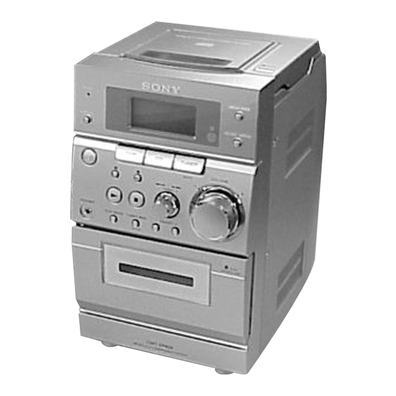
HCD-EP404
CD
SECTION
TAPE DECK
SECTION
SPECIFICATIONS
(8Ω at 1 kHz, DIN)
8 + 8 W
(8Ω at 1 kHz, 10% THD)
16 + 16 W
Accepts headphones of
8Ω or more
Accepts impedance of 8 to
16Ω
Compact disc and digital
audio system
Semiconductor laser
(λ =780 nm)
Emission duration:
continuous
20 Hz - 20 kHz (±0.5 dB)
4-track 2-channel stereo
50 - 13 000 Hz (±3 dB),
using Sony TYPE I
cassette
COMPACT DISC DECK RECEIVER
Model Name Using Similar Mechanism
CD Mechanism Type
Model Name Using Similar Mechanism
Tape Transport Mechanism Type
Tuner section
FM stereo, FM/AM superheterodyne tuner
FM tuner section
Tuning range
87.5 - 108.0 MHz
Antenna
FM lead antenna
Intermediate frequency
10.7 MHz
AM tuner section
Tuning range
531 -1 602 kHz
(with the interval set at
9 kHz)
Antenna
Built-in ferrite bar antenna
Intermediate frequency
450 kHz
General
Power requirements
230 V AC, 50/60 Hz
Power consumption
38W
0.5 W (in the standby
mode)
Approx. 145 × 240 × 252 mm
Dimensions (w/h/d):
Mass:
3.1 kg
Design and specifications are subject to change
without notice.
AEP Model
UK Model
HCD-EP50
CS-21SC-1280
NEW
CFL4318
Advertisement
Table of Contents

Related Manuals for Sony HCD-EP404


Summary of Contents for Sony HCD-EP404
- Page 1 HCD-EP404 SERVICE MANUAL AEP Model UK Model Ver 1.1 2002. 07 HCD-EP404 is the amplifler, CD player, tape deck and tuner section in CMT-EP404. Model Name Using Similar Mechanism HCD-EP50 SECTION CD Mechanism Type CS-21SC-1280 Model Name Using Similar Mechanism...
-
Page 2: Table Of Contents
COMPONENTS IDENTIFIED BY MARK 0 OR DOTTED LINE WITH MARK 0 ON THE SCHEMATIC DIAGRAMS AND IN THE PARTS LIST ARE CRITICAL TO SAFE OPERATION. REPLACE THESE COMPONENTS WITH SONY PARTS WHOSE PART NUMBERS APPEAR AS SHOWN IN THIS MANUAL OR IN SUPPLEMENTS PUBLISHED BY SONY. -
Page 3: Servicing Notes
HCD-EP404 SECTION 1 SERVICING NOTES LASER DIODE AND FOCUS SEARCH OPERATION NOTES ON HANDLING THE OPTICAL PICK-UP CHECK BLOCK OR BASE UNIT Press the ?/1 button to the power ON with no disc inserted The laser diode in the optical pick-up block may suffer electrostatic and press the CD button. -
Page 4: General
HCD-EP404 SECTION 2 GENERAL This section is extracted from instruction manual. Main unit BUTTON DESCRIPTIONS ALPHABETICAL ORDER P – Z @/1 (power) wd (7, 16, 18) A – M PHONES jack qk Cassette compartment qg (14) PLAY MODE qj (8, 9) CD 4 (8, 9, 15) . -
Page 5: Remote Control
HCD-EP404 Remote control ALPHABETICAL ORDER BUTTON DESCRIPTIONS m (rewind) M (fast forward) P – Z A – M ql (8, 14) PLAY MODE 7 (8, 9, 13, 14, 15) CD wf (8, 9, 15) . (go back) > (go forward) PRESET +/–... -
Page 6: Disassembly
HCD-EP404 Ver 1.1 2002.07 SECTION 3 DISASSEMBLY • The equipment can be removed using the following procedure. 3-1. FRONT PANEL SECTION 3-8. CASSETE LID (Page 6) (Page 10) 3-4. POWER BOARD, 3-2. MAIN BOARD 3-6. CD CABINET SECTION POWER TRANSFORMER... -
Page 7: Main Board
HCD-EP404 Ver 1.1 2002.07 3-2. MAIN Board q; MAIN board 8 screw (+BTP2.6 × 8) 1 connector (CN704) 2 connector (CN705) 4 connector (CN701) 3 connector (CN601) 5 connector (CN402) 9 claw 7 connector (CN702) 6 connector (CN703) 3-3. Tape Mechanism Deck (CFL4318) 2 two screws (+BVTP3 ×... -
Page 8: Power Board, Power Transformer
HCD-EP404 3-4. POWER Board, Power Transformer rear cabinet assy 2 ac cord holder 1 screw (+BVTP3 × 10) 9 power pwb mounting bkt 3 screw 6 Remove four solderings. (+BVTP3 × 10) 4 four screws (+BVTP3 × 12) 8 screw (+BTP2.6 ×... -
Page 9: Cd Cabinet Section
HCD-EP404 3-6. CD Cabinet Section 2 CD cabinet section 1 two screws (+BTP2.6 × 8) 3-7. CD Mechanism Deck (CS-21SC-1280) qd vibration proof rubber 9 two spring clamps (orange) qf CD mechanism deck (CS-21SC-1280) 8 two spring clamps qs vibration proof rubber... -
Page 10: Cassette Lid
HCD-EP404 3-8. Cassette Lid 3 claw 3 claw 1 Push open/close switch 5 cassette lid... -
Page 11: Mechanical Adjustments
HCD-EP404 SECTION 4 SECTION 5 MECHANICAL ADJUSTMENTS ELECTRICAL ADJUSTMENTS PRECAUTION PRECAUTION Clean the following parts with a denatured-alcohol-moistened Setting swab : MEGA BASS switch : OFF record/playback head pinch roller erase head rubber belts TAPE DECK SECTION 0 dB=0.775 V... - Page 12 HCD-EP404 Tape Speed Adjustment Adjustment Location: Record/Playback Head. Setting: Function: TAPE test tape WS-48B frequency counter (3 kHz, 0 dB) 32 Ω – HEADPHONE board PHONES jack (JK501) Procedure: Playback WS-48B (tape center). Adjsut the volume in CAPSTAN/REEL motor so that the frequency counter reading becomes 3,000 Hz.
- Page 13 HCD-EP404 0 dB=1 µV TUNER SECTION AM FREQUENCY COVERAGE ADJUSTMENT Adjustment Part Frequency Display Reading on Digital Voltmeter [AM] 1.5 ± 0.2 V Confirmation 531 kHz Setting: 7.3 ± 0.3 V T101 1,602 kHz Function : TUNER Band switch : AM...
- Page 14 HCD-EP404 Adjustment Location and Connecting Points – MAIN BOARD (Component Side) – – MAIN BOARD (Conductor Side) – L104 AM Tracking TC102 Adjustment TP(AM VT) IC101 T101 AM Frequency Coverage Adjustment (FM VT) L103 FM Frequency Coverage Adjustment TC102 FM Tracking...
-
Page 15: Diagrams
HCD-EP404 SECTION 6 DIAGRAMS Note on Printed Wiring Board: Note on Schematic Diagram: 6-1. Circuit Boards Location • All capacitors are in µF unless otherwise noted. p: pF. • W : indicates side identified with part number. • : Pattern from the side which enables seeing. -
Page 16: Block Diagrams
HCD-EP404 6-2. Block Diagrams TUNER/TAPE DECK Section AM TRACKING IC101 TC102 L104 AM/FM IF AMP, AM ANT TUNER MIX, MPX, DET, OSC L-CH AMRF_IN L_OUT T102 F103 SECTION 450kHz D105 T101 AM_MIX AM_IF X101 AM FREQUENCY AM OSC 10.7MHz COVERAGE... -
Page 17: Amp Section
HCD-EP404 AMP Section JK501 PHONES IC401 FUNCTION SELECT SWITCH, ELECTRONIC VOLUME TUNER TUNER L-CH LVROUT SECTION IC601 R-CH R-CH POWER AMP R-CH STK601 TAPE TL-CH LVRIN D402 SECTION TR-CH Q401 R-CH MEGA BASS CD L-IN D401 – LTOUT D403 SPEAKER... -
Page 18: Display/Power Section
HCD-EP404 DISPLAY/POWER Section IC301 (3/3) SYSTEM CONTROLLER, LIQUID CRYSTAL DISPLAY DRIVER X302 REMOTEIN REMOTE CONTROL Q604 RECEIVER CD9V REGULATOR D601 Q605,606 CD-EN REGULATOR CONTROL SWITCH ENCODERA X303 ROTARY T201 ENCODER VOLUME ENCODERB POWER D901 – 903 TRANSFORMER (LCD BACK LIGHT) -
Page 19: Printed Wiring Board Main Section
HCD-EP404 6-3. Printed Wiring Board MAIN Section • See page 15 for Circuit Boards Location. • Semiconductor MAIN BOARD (RECORD/PLAYBACK HEAD) L104 Location AM FERRITE-ROD ANTENNA (L-CH) Ref. No. Location D101 (R-CH) D102 IC701 D103 D104 (ERASE HEAD) D105 (ERASE) -
Page 20: Schematic Diagram Main Section (1/3)
HCD-EP404 6-4. Schematic Diagram MAIN Section (1/3) • See page 15 for Waveforms. • See page 27,28 for IC Block Diagrams. L104, TC102 L103 T101 MAIN BOARD (1/3) AM TRACKING FM FREQUENCY AM FREQUENCY COVERAGE COVERAGE L102, TC101 FM TRACKING... -
Page 21: Schematic Diagram Main Section (2/3)
HCD-EP404 6-5. Schematic Diagram MAIN Section (2/3) • See page 15 for Waveforms. • See page 28 for IC Block Diagrams. MAIN BOARD (2/3) IC701 IC702 2SC945 REC/PB ALC, REC/PB SWITCH REC,PB AMP SWITCH [0.1] 0 [0.1] [1.9] [1.9] 0.6 [0] [0.7]... -
Page 22: Schematic Diagram Main Section (3/3)
HCD-EP404 6-6. Schematic Diagram MAIN Section (3/3) MAIN BOARD (3/3) IC601 HEADPHONE BOARD 27.6 POWER AMP 13.5 MAIN BOARD 13.5 PHONES (1/3) 13.7 SPEAKER (IMPEDANCE USE 8 ) MAIN BOARD (2/3) MAIN BOARD 2SC3623 (1/3) (2/3) 0 <8.7> 14.2 +5V REG 12.1... -
Page 23: Printed Wiring Board Panel Section
HCD-EP404 6-7. Printed Wiring Board PANEL Section • See page 15 for Circuit Boards Location. DISPLAY BOARD • Semiconductor Location Ref. No. Location D302 TIMER D303 (LIQUID CRYSTAL DISPLAY) D305 D308 D309 LED BOARD MEGA D310 BASS D312 IC301 D313... -
Page 24: Schematic Diagram Panel Section
HCD-EP404 6-8. Schematic Diagram PANEL Section • See page 15 for Waveforms. • See page 29 for IC Pin Function Description. DISPLAY BOARD (LIQUID CRYSTAL DISPLAY) PLAY TAPE TUNER MODE TUNER MEM ENTER DISPLAY PRESET+ PRESET- TIMER TUNING+ TUNING- SEL2215S... -
Page 25: Printed Wiring Board Power Section
HCD-EP404 6-9. Printed Wiring Board POWER Section • See page 15 for Circuit Boards Location. POWER BOARD T201 POWER TRANSFORMER • Semiconductor Location Ref. No. Location D201 D202 D203 D204 D205 D206 D207 D208 D212 D213 D215 D216 D217 D218... -
Page 26: Schematic Diagram Power Section
HCD-EP404 6-10. Schematic Diagram POWER Section POWER BOARD 22000p POWER TRANSFORMER 22000p 22000p AC IN 22000p MAIN BOARD (3/3) 22000p (Page 22) 2SA608SP-G Q205,206 POWER ON/OFF RELAY DRIVE 2SC536NP-F POWER TRANSFORMER MTZJ-T- 72-6.2B 22000p 22000p 22000p 22000p No mark : FM 22000p MTZJ-T-72-6.8B... - Page 27 HCD-EP404 • IC Block Diagrams – MAIN Board – IC101 LA1823 GND2 VCC2 MUTE PHASE PILOT DECODER COMP ST SW TRIG S-METER BUFFER BUFFER VCC1 GND1 IC102 LC72131 PHASE DETECTOR CHARGE PUMP POWER REFERENCE UNLOCK DIVIDER DETECTOR RESET SWALLOW COUNTER...
- Page 28 HCD-EP404 IC401 LC75392 LVROUT RVROUT LVRIN RVRIN LTOUT RTOUT – LTCOM RTCOM LATCH DECODER SHIFT REGISTER VREF CONTROL IC701 uPC1330HA-NA IC702 AN7312 RIPPLE FILTER INVERTER AMP. CH2 AMP. CH1 COMPARATER SW P1 CONT GND SW R1 GND SW P2 GND...
-
Page 29: Ic Pin Function Description
HCD-EP404 6-12. IC Pin Function Description • IC301 µPD780306GC-A68-8EU System Controller, Liquid Crystal Display Driver (DISPLAY Board) Pin No. Pin Name Description Key input terminal (A/D input) SW306 to SW309 (x , X , N , TUNER MEM/ENTER)keys input KEY2 KEY3 Key input terminal (A/D input) SW310 to SW312 (PRESET +/–, DISPLAY)keys input... - Page 30 HCD-EP404 Pin No. Pin Name Description Sub system clock output terminal (32.768 kHz) Not used (open) System reset signal input from the reset signal generator (IC304) “L ”:reset RESET For several hundreds msec. after the power supply rises, “L ” is input, then it changes to “H ”...
-
Page 31: Exploded Views
HCD-EP404 SECTION 7 EXPLODED VIEWS NOTE: • -XX, -X mean standardized parts, so they may • Items marked “*” are not stocked since they The components identified by mark 0 or have some differences from the original one. are seldom required for routine service. Some dotted line with mark 0 are critical for safety. -
Page 32: Front Panel Section -1
HCD-EP404 Ver 1.1 2002.07 7-2. Front Panel Section -1 supplied including X303 Ref. No. Part No. Description Remarks Ref. No. Part No. Description Remarks 4-241-113-01 VOL.ROTARY KNOB 4-236-905-01 CASS LATCH SPRING 4-241-112-01 VOL.DECORATION RING 4-236-907-01 CASS LID LATCH HOLDER 4-241-380-01 DISPLAY WINDOW... -
Page 33: Front Panel Section -2
HCD-EP404 7-3. Front Panel Section -2 supplied not supplied CN301 Ref. No. Part No. Description Remarks Ref. No. Part No. Description Remarks 4-235-995-01 RUBBER FOOT 4-240-272-01 FUNCTION KNOB 4-241-382-01 FRONT PANEL 4-240-227-01 LCD DEFUSE SHEET A-4729-694-A HEADPHONE BOARD, COMPLETE 4-240-243-01 LCD LIGHT GUIDE... -
Page 34: Cd Cabinet Section
HCD-EP404 7-4. CD Cabinet Section SW600 Ref. No. Part No. Description Remarks Ref. No. Part No. Description Remarks 4-240-255-01 CD COVER HOUSING 4-235-949-01 PU COVER 0 166 4-236-280-01 RUBBER, VIBRATION PROOF (PINK) 1-796-189-11 MECH, CD 4-235-991-01 PULLEY SCREW 4-236-281-01 RUBBER, VIBRATION PROOF (ORG) -
Page 35: Electrical Parts List
HCD-EP404 SECTION 8 DISPLAY ELECTRICAL PARTS LIST NOTE: • Due to standardization, replacements in the • RESISTORS When indicating parts by reference number, parts list may be different from the parts All resistors are in ohms. please include the board name. - Page 36 HCD-EP404 DISPLAY HEADPONE Ref. No. Part No. Description Remarks Ref. No. Part No. Description Remarks R321 1-216-821-11 METAL CHIP 1/16W R396 1-249-417-11 CARBON 1/4W F R322 1-216-832-11 METAL CHIP 8.2K 1/16W R397 1-249-417-11 CARBON 1/4W F R323 1-216-832-11 METAL CHIP 8.2K...
- Page 37 HCD-EP404 MAIN Ref. No. Part No. Description Remarks Ref. No. Part No. Description Remarks A-4729-695-A MAIN BOARD, COMPLETE C161 1-115-339-11 CERAMIC CHIP 0.1uF 10.00% 50V C162 1-115-339-11 CERAMIC CHIP 0.1uF 10.00% 50V ********************* C163 1-163-009-91 CERAMIC CHIP 0.001uF 10.00% 50V...
- Page 38 HCD-EP404 MAIN Ref. No. Part No. Description Remarks Ref. No. Part No. Description Remarks C615 1-104-665-11 ELECT 100uF 20.00% 25V C756 1-126-960-11 ELECT 20.00% 50V C616 1-162-970-11 CERAMIC CHIP 0.01uF C757 1-126-960-11 ELECT 20.00% 50V C758 1-126-960-11 ELECT 20.00% 50V...
- Page 39 HCD-EP404 MAIN Ref. No. Part No. Description Remarks Ref. No. Part No. Description Remarks < RESISTOR > R108 1-216-095-00 METAL CHIP 1/10W R109 1-216-797-11 METAL CHIP 1/16W J401 1-249-425-11 CARBON 4.7K 1/4W F R111 1-216-085-91 RES-CHIP 1/10W < COIL >...
- Page 40 HCD-EP404 MAIN Ref. No. Part No. Description Remarks Ref. No. Part No. Description Remarks R428 1-216-069-00 METAL CHIP 6.8K 1/10W R723 1-216-095-00 METAL CHIP 1/10W R429 1-216-057-00 METAL CHIP 2.2K 1/10W R430 1-216-057-00 METAL CHIP 2.2K 1/10W R724 1-216-095-00 METAL CHIP...
- Page 41 HCD-EP404 Ver 1.1 2002.07 MAIN POWER Ref. No. Part No. Description Remarks Ref. No. Part No. Description Remarks < TERMINAL > D206 8-719-200-02 DIODE 1N4001 D207 8-719-200-02 DIODE 1N4001 SPK601 1-537-238-11 TERMINAL BOARD (SPEAKER) D208 8-719-200-02 DIODE 1N4001 D212 8-719-991-33 DIODE 1N4148TP <...
- Page 42 HCD-EP404 REVISION HISTORY Clicking the version allows you to jump to the revised page. Also, clicking the version at the upper right on the revised page allows you to jump to the next revised page. Ver. Date Description of Revision 2002.04...
Need help?
Do you have a question about the HCD-EP404 and is the answer not in the manual?
Questions and answers