Table of Contents
Advertisement
QQ
3 7 63 1515 0
SERVICE MANUAL
Ver 1.0 2001.04
HCD-VX777 is the tuner, deck, CD and amplifier
section in MHC-VX777.
TE
L 13942296513
VIDEO CD/CD player section
System
Laser
Laser Output
Frequency response
Wave length
Signal-to-noise ratio
Dynamic range
Video color system format
CD OPTICAL DIGITAL OUT
(Square optical connector jack, rear panel)
Wave length
Output level
Tape player section
Recording system
Frequency response
(DOLBY NR OFF*)
Wow and flutter
* HCD-VX777 only
www
.
Sony Corporation
9-873-850-11
2001D0900-1
Home Audio Company
© 2001.4
Shinagawa Tec Service Manual Production Group
http://www.xiaoyu163.com
TAPE DECK
Compact disc and digital audio system
Semiconductor laser (λ=780nm)
Max. 44.6 µW*
*This output is the value measured at a
distance of 200 mm from the objective
lens surface on the Optical Pick-up
Block with 7 mm aperture.
2 Hz — 20 kHz (–0.5 dB)
780 — 790 nm
More than 90 dB
More than 90 dB
660 nm
—18 dBm
4-track 2-channel stereo
40 — 13,000 Hz (–3 dB), using
Sony TYPE I cassette
40 — 14,000 Hz (–3 dB), using
Sony TYPE II cassette*
–0.15% W.Peak (IEC)
0.1% W.RMS (NAB)
–0.2% W.Peak (DIN)
x
ao
u163
y
i
http://www.xiaoyu163.com
HCD-VX777
2 9
8
Model Name Using Similar Mechanism
CD Mechanism Type
CD
SECTION
Base Unit Type
Optical Pick-up Type
Model Name Using Similar Mechanism
Q Q
SECTION
Tape Transport Mechanism Type
3
6 7
1 3
SPECIFICATIONS
Tuner section
FM stereo, FM/AM superheterodyne tuner
FM tuner section
Tuning range
Antenna
Antenna terminals
Intermediate frequency
AM tuner section
Tuning range
Latin American models:
PAL
Middle Eastern models:
Other models:
Antenna
Antenna terminals
Intermediate frequency
COMPACT DISC DECK RECEIVER
.
9 4
2 8
HCD-DX70
CDM58E-30BD61A
BU-30BD61A
A-MAX.3
NEW
TCM-230AWR41/MWR41
1 5
0 5
8
2 9
9 4
87.5 — 108.0 MHz
FM lead antenna
75 ohm unbalanced
10.7 MHz
530 — 1,710 kHz
(with the interval set at 10 kHz)
531 — 1,710 kHz
(with the interval set at 9 kHz)
531 — 1,602 kHz
(with the interval set at 9 kHz)
531 — 1,602 kHz
(with the interval set at 9 kHz)
530 — 1,710 kHz
(with the interval set at 10 kHz)
AM loop antenna
External antenna terminal
450 kHz
— Continued on next page —
m
co
9 9
E Model
2 8
9 9
Advertisement
Table of Contents

Related Manuals for Sony HCD-VX777


Summary of Contents for Sony HCD-VX777
- Page 1 HCD-VX777 3 7 63 1515 0 SERVICE MANUAL E Model Ver 1.0 2001.04 HCD-VX777 is the tuner, deck, CD and amplifier section in MHC-VX777. Model Name Using Similar Mechanism HCD-DX70 CD Mechanism Type CDM58E-30BD61A SECTION Base Unit Type BU-30BD61A Optical Pick-up Type A-MAX.3...
-
Page 2: Table Of Contents
HCD-VX777 3 7 63 1515 0 TABLE OF CONTENTS General Power requirements Australian models: 230 — 240 V AC, 1. GENERAL ·········································································· 4 50/60 Hz Mexican models: 120 V AC, 60 Hz 2. DISASSEMBLY Thailand models: 220 V AC, 50/60 Hz... - Page 3 HCD-VX777 3 7 63 1515 0 SETTING THE TIME NOTES ON HANDLING THE OPTICAL PICK-UP BLOCK OR BASE UNIT Turn on the system. The laser diode in the optical pick-up block may suffer electrostatic Press CLOCK/TIMER SET on the remote.
-
Page 4: General
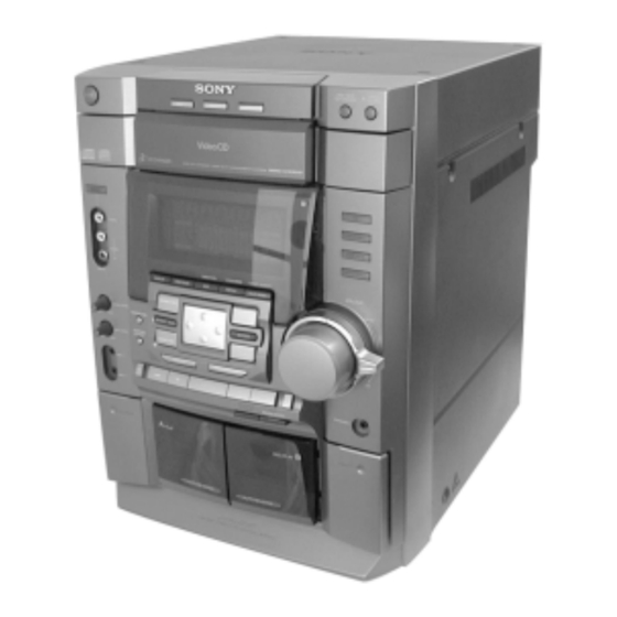
HCD-VX777 SECTION 1 GENERAL 3 7 63 1515 0 Front Panel 2 3 4 w; wa ws wd wf wg elek eh eg ed ea wl ef es L 13942296513 Location of Parts and Controls 1 @/1 (POWER) button and indicator... -
Page 5: Disassembly
HCD-VX777 SECTION 2 3 7 63 1515 0 DISASSEMBLY • The equipment can be removed using the following procedure. Case (Top) Loading Panel Front Panel Section Tape Mechanism Deck Head (A) Board, Head (B) Board And SW Board CD SW Board, Panel Board And PAD Switch Board... -
Page 6: Loading Panel
HCD-VX777 3 7 63 1515 0 2-2. LOADING PANEL 4 Pull-out the disc tray. CD mechanism deck (CDM58) 1 Turn the pulley to the direction of arrow. Front panel side pulley 2 Pull-out the disc tray. L 13942296513 2-3. FRONT PANEL SECTION qdscrew (+BVTP 3 ×... -
Page 7: Tape Mechanism Deck
HCD-VX777 3 7 63 1515 0 2-4. TAPE MECHANISM DECK 1five screws (+BVTP 2.6 × 8) 2Tape mechanism deck L 13942296513 2-5. CD SW BOARD, PANEL BOARD, PAD SWITCH BOARD 3CD SW board 1four screws (+BVTP 2.6 × 8) -
Page 8: Main Trans Board
HCD-VX777 3 7 63 1515 0 2-6. MAIN TRANS BOARD 9panel, back 4connector (CN403) 5connector (CN973) qdMAIN TRANS board 8five screws (+BVTP 3 × 10) 1screw (+BVTP 3 × 8) 6connector (CN977) qatwo screws (+BVTT 4 × 8) 0two screws (+BVTT 4 × 8) -
Page 9: Leaf Sw Board, Head (A) Board, Head (B) Board
HCD-VX777 3 7 63 1515 0 2-8. LEAF SW BOARD, HEAD (A) BOARD, HEAD (B) BOARD 1five claws 2LEAF SW board 3Remove the four solderings. 5HEAD (A) board 7HEAD (B) board 4screw (+PTT 2 × 4), ground point 6screw (+PTT 2 × 4),... -
Page 10: Video Board
HCD-VX777 3 7 63 1515 0 2-10. DRIVER BOARD, MOTOR BOARD, CD SENSOR BOARD AND VIDEO BOARD 0screw (+PTPWH 2.6 × 8) 5two screws (+BVTP 2.6 × 8) 7MOTOR board 8flat type wire (CN721) 6Remove the two solderings of motor. -
Page 11: Test Mode
HCD-VX777 SECTION 3 TEST MODE 3 7 63 1515 0 [Cold Reset] 7. In the key check mode, the fluorescent indicator tube displays • The cold reset clears all data including preset data stored in the “K0 V0”. Each time a button is pressed, “KEY” value increases. - Page 12 HCD-VX777 3 7 63 1515 0 * Tape function How to exit the CD aging mode: Press the ?/1 and turn off the main power. 1. When a tape is inserted in Deck B and recording is started, the input source function selects VIDEO automatically.
- Page 13 HCD-VX777 3 7 63 1515 0 [ VIDEO BOARD ] (SIDE A) 1 2 3 J301 CN301 CN501 SL503 SL502 SL501 CN503 CHECK LED CN502 L 13942296513 u163 http://www.xiaoyu163.com...
-
Page 14: Mechanical Adjustments
HCD-VX777 SECTION 4 SECTION 5 MECHANICAL ADJUSTMENTS ELECTRICAL ADJUSTMENTS 3 7 63 1515 0 Precaution DECK SECTION 0 dB=0.775 V 1. Clean the following parts with a denatured alcohol-moistened swab: 1. Demagnetize the record/playback head with a head record/playback heads pinch rollers demagnetizer. - Page 15 HCD-VX777 3 7 63 1515 0 2. Turn the adjustment screw and check output peaks. If the peaks DECK B Tape Speed Adjustment do not match for L-CH and R-CH, turn the adjustment screw Note: Start the Tape Speed adjustment as below after setting to the test mode.
- Page 16 HCD-VX777 3 7 63 1515 0 DECK B REC Bias Adjustment 4. Mode: Record Procedure: INTRODUCTION MD/VIDEO (AUDIO) IN When set to the test mode performed in Tape Speed Adjustment, 315 Hz, 50 mV (–23.8 dB) AF OSC when the tape is rewound after recording, the “REC memory mode”...
- Page 17 HCD-VX777 3 7 63 1515 0 FM Tuned Level Adjustment CD SECTION FM RF SSG Note : 1. CD Block is basically designed to operate without adjustment. 75 Ω coaxial Therefore, check each item in order given. 2. Use LUV-P01 (4-999-032-01) unless otherwise indicated.
- Page 18 HCD-VX777 3 7 63 1515 0 Note: Clear RF signal waveform means that the shape “◊” can be VIDEO SECTION clearly distinguished at the center of the waveform. Frequency adjustment RF signal waveform VOLT/DIV : 200mV Connect the frequency counter to check point of the VIDEO TIME/DIV : 500ns board.
-
Page 19: Diagrams
HCD-VX777 SECTION 6 3 7 6 3 1 5 1 5 0 DIAGRAMS 6-1. CIRCUIT BOARD LOCATION THIS NOTE IS COMMON FOR PRINTED WIRING BOARDS AND SCHEMATIC DIAGRAMS. (In addition to this, the necessary note is printed in each block.) - Page 20 HCD-VX777 3 7 6 3 1 5 1 5 0 • WAVEFORMS – PANEL BOARD – – BD BOARD – – MAIN BOARD – – VIDEO BOARD – IC601 is (XOUT) IC502 qd IC509 ql IC501 qa (XC-OUT) T301 4...
-
Page 21: Block Diagrams
HCD-VX777 6-2. BLOCK DIAGRAMS 3 7 6 3 1 5 1 5 0 – TUNER/CD SECTION – VX777 MODEL AM/FM IF MPX LPF11 IC11 RF IF • RCH is omitted BUFFER L-CH ANT IN IF OUT FM IF L OUT •... - Page 22 HCD-VX777 3 7 6 3 1 5 1 5 0 – VIDEO SECTION – D-RAM IC507 IC506 2 - 10 31 - 39 25 4 28 29 3 2 30 12 - 5 27 26 23 13 14 28 29...
- Page 23 HCD-VX777 3 7 6 3 1 5 1 5 0 – MAIN SECTION – J102 SURROUND SPEAKER R CH INPUT SELECT TONE/VOL CONT IC101 IC102 IC501 TM801 TUNER L-CH SECTION IN2A VOL OUT2 (Page 21) POWER SPEAKER Q504,505 Q861...
-
Page 24: Schematic Diagram - Bd Section
HCD-VX777 3 7 6 3 1 5 1 5 0 6-3. SCHEMATIC DIAGRAM – BD SECTION – • See page 20 for Waveforms. • See page 58, 59 for IC Block Diagrams. • See page 48 for IC Pin Function. -
Page 25: Printed Wiring Board - Bd Section
HCD-VX777 3 7 6 3 1 5 1 5 0 6-4. PRINTED WIRING BOARD – BD SECTION – • See page 19 for Circuit Boards Location. 1 3 9 4 2 2 9 6 5 1 3 (Page 26) •... -
Page 26: Printed Wiring Board - Video Section
HCD-VX777 3 7 6 3 1 5 1 5 0 6-5. PRINTED WIRING BOARD – VIDEO SECTION – • See page 19 for Circuit Boards Location. 1 3 9 4 2 2 9 6 5 1 3 (Page 25) (Page 30) •... -
Page 27: Schematic Diagram - Video (1/3) Section
HCD-VX777 3 7 6 3 1 5 1 5 0 6-6. SCHEMATIC DIAGRAM – VIDEO (1/3) SECTION – • See page 20 for Waveforms. • See page 52 for IC Pin Function. TP523 (Page 24) 1 3 9 4 2 2 9 6 5 1 3... -
Page 28: Schematic Diagram - Video (2/3) Section
HCD-VX777 3 7 6 3 1 5 1 5 0 6-7. SCHEMATIC DIAGRAM – VIDEO (2/3) SECTION – • See page 20 for Waveforms. • See page 54 for IC Pin Function. (Page 27) (Page 29) 1 3 9 4 2 2 9 6 5 1 3... -
Page 29: Q Q 6-8. Schematic Diagram - Video (3/3) Section
HCD-VX777 3 7 6 3 1 5 1 5 0 6-8. SCHEMATIC DIAGRAM – VIDEO (3/3) SECTION – • See page 20 for Waveforms. • See page 60 for IC Block Diagrams. (Page 35) IC B/D 1 3 9 4 2 2 9 6 5 1 3... -
Page 30: Printed Wiring Boards - Main Section
HCD-VX777 3 7 6 3 1 5 1 5 0 6-9. PRINTED WIRING BOARD – MAIN SECTION – • See page 19 for Circuit Boards Location. (Page 44) (Page 26) • Semiconductor Location Ref. No. Location Ref. No. Location... -
Page 31: Schematic Diagram - Main (1/4) Section
HCD-VX777 3 7 6 3 1 5 1 5 0 6-10. SCHEMATIC DIAGRAM – MAIN (1/4) SECTION – • See page 57 for IC Block Diagrams. IC B/D FM TUNED LEVEL 1 3 9 4 2 2 9 6 5 1 3... -
Page 32: Schematic Diagram - Main (2/4) Section
HCD-VX777 3 7 6 3 1 5 1 5 0 6-11. SCHEMATIC DIAGRAM – MAIN (2/4) SECTION – (Page 35) (Page 27) (Page 31) 1 3 9 4 2 2 9 6 5 1 3 IC B/D (Page 34) -
Page 33: Schematic Diagram - Main (3/4) Section
HCD-VX777 3 7 6 3 1 5 1 5 0 6-12. SCHEMATIC DIAGRAM – MAIN (3/4) SECTION – • See page 20 for Waveforms. • See page 57 for IC Block Diagrams. (Page 32) C149 470P RV302 PB LEVEL (L) -
Page 34: Schematic Diagram - Main (4/4) Section
HCD-VX777 3 7 6 3 1 5 1 5 0 6-13. SCHEMATIC DIAGRAM – MAIN (4/4) SECTION – • See page 20 for Waveforms. • See page 49 for IC Pin Function. (Page 37) (Page 37) (Page 32) (Page 33) -
Page 35: Schematic Diagram - Switch Section
HCD-VX777 3 7 6 3 1 5 1 5 0 6-14. SCHEMATIC DIAGRAM – SWITCH SECTION – • See page 20 for Waveforms. 6-15. PRINTED WIRING BOARD – SWITCH SECTION – • See page 19 for Circuit Boards Location. -
Page 36: Printed Wiring Boards - Power Amp Section
HCD-VX777 6-16. PRINTED WIRING BOARDS – POWER AMP SECTION – • See page 19 for Circuit Boards Location. 3 7 6 3 1 5 1 5 0 (Page 30) (Page 30) • Semiconductor Location Ref. No. Location D501 (Page 46) -
Page 37: Schematic Diagram - Power Amp Section
HCD-VX777 3 7 6 3 1 5 1 5 0 6-17. SCHEMATIC DIAGRAM – POWER AMP SECTION – (Page 47) 1 3 9 4 2 2 9 6 5 1 3 (Page 47) w w w u 1 6 3... -
Page 38: Printed Wiring Boards - Panel Section
HCD-VX777 3 7 6 3 1 5 1 5 0 6-18. PRINTED WIRING BOARD – PANEL SECTION – • See page 19 for Circuit Boards Location. (Page 40) • Semiconductor Location Ref. No. Location D604 D605 D606 D607 D608... -
Page 39: Schematic Diagram - Panel Section
HCD-VX777 3 7 6 3 1 5 1 5 0 6-19. SCHEMATIC DIAGRAM – PANEL SECTION – • See page 20 for Waveforms. • See page 59 for IC Block Diagrams. • See page 51 for IC Pin Function. -
Page 40: Printed Wiring Boards - Cd Sw/Pad Section
HCD-VX777 6-20. PRINTED WIRING BOARDS – CD-SW/PAD SWITCH SECTION – • See page 19 for Circuit Boards Location. 3 7 6 3 1 5 1 5 0 • Semiconductor Location Ref. No. Location D791 D792 D793 D794 A-10 Q791... -
Page 41: Schematic Diagram - Cd Sw/Pad Section
HCD-VX777 3 7 6 3 1 5 1 5 0 6-21. SCHEMATIC DIAGRAM – CD SW/PAD SWITCH SECTION – (Page 39) 1 3 9 4 2 2 9 6 5 1 3 w w w (Page 39) u 1 6 3... -
Page 42: Printed Wiring Boards - Leaf Sw Section
HCD-VX777 3 7 6 3 1 5 1 5 0 6-22. PRINTED WIRING BOARDS – LEAF SW SECTION – • See page 19 for Circuit Boards Location. • Semiconductor Location Ref. No. Location D1001 D1002 IC1001 IC1002 Q1001 (Page 30) -
Page 43: Schematic Diagram - Leaf Sw Section
HCD-VX777 3 7 6 3 1 5 1 5 0 6-23. SCHEMATIC DIAGRAM – LEAF SW SECTION – 1 3 9 4 2 2 9 6 5 1 3 (4/4) (Page 34) w w w u 1 6 3... -
Page 44: Printed Wiring Boards - Driver Section
HCD-VX777 3 7 6 3 1 5 1 5 0 6-24. PRINTED WIRING BOARDS – DRIVER SECTION – • See page 19 for Circuit Boards Location. • Semiconductor Location Ref. No. Location D701 IC701 IC711 1 3 9 4 2 2 9 6 5 1 3 There are a few cases that the part isn’t mounted... -
Page 45: Schematic Diagrams - Driver Section
HCD-VX777 3 7 6 3 1 5 1 5 0 6-25. SCHEMATIC DIAGRAMS – DRIVER SECTION – • See page 50 for IC Block Diagrams. IC B/D (2/4) (Page 32) 1 3 9 4 2 2 9 6 5 1 3... -
Page 46: Printed Wiring Boards - Trans Section
HCD-VX777 6-26. PRINTED WIRING BOARDS – TRANS SECTION – • See page 19 for Circuit Boards Location. 3 7 6 3 1 5 1 5 0 (Page 36) 1 3 9 4 2 2 9 6 5 1 3 (Page 36) •... -
Page 47: Schematic Diagram - Trans Section
HCD-VX777 3 7 6 3 1 5 1 5 0 6-27. SCHEMATIC DIAGRAM – TRANS SECTION – (Page 37) 1 3 9 4 2 2 9 6 5 1 3 (Page 37) w w w u 1 6 3... -
Page 48: Ic Pin Functions
HCD-VX777 3 7 6 3 1 5 1 5 0 6-28. IC PIN FUNCTIONS • IC101 DIGITAL SIGNAL PROCESSOR (CXD3068Q) (BD Board) Pin No. Pin Name Description Pin No. Pin Name Description AUDIO-OUT Audio out ON/OFF signal (H=ON,L=OFF) A-TRG... - Page 49 HCD-VX777 3 7 63 1515 0 • IC501 MASTER CONTROL (M30620MCA-A95FP) (MAIN BOARD) Pin No. Pin Name Function AUDIO OUT ON/OFF AUDIO OUT signal output. H=ON, L=OFF. STEREO STEREO detect signap input. L=ON, H=OFF. TUNED TUNED SIRCS SUR1 Surround control signal output.
- Page 50 HCD-VX777 3 7 63 1515 0 Pin No. Pin Name Function CAPM-H/L Capstan motor High/Low speed control signal output. CAPM-CONTROL Capstan motor REV/FWD/STOP control signal output. H=REV, L=FWD/STOP. A-PLAY A deck play detect signal input. B-PLAY B deck play detect signal input.
- Page 51 HCD-VX777 3 7 63 1515 0 • IC601 DISPLAY CONTROL (MB90M407PF-G-107-BND) PANEL Board Pin No. Pin Name Function 1 to 5 G5 to G1 FL gride signal output. 6 to 10 P1 to P5 FL segment signal output. VSS-IO —...
- Page 52 HCD-VX777 3 7 63 1515 0 • IC502 VIDEO CD CONTROL (M30622MGA-A45FP) (VIDEO Board (1/3)) Pin No. Pin Name Function SENSE Internal state (SENSE) monitor input (IC101) SENSE CLK Serial data reading clock output (IC101) RESOLUTION Serial data output (IC101)
- Page 53 HCD-VX777 3 7 63 1515 0 Pin No. Pin Name Function INSW Not used OUTSW Not used MODEL 1 L : System input (Fixed at “L”) MODEL 2 L : System input (Fixed at “L”) TBLL Not used TBLR...
- Page 54 HCD-VX777 3 7 63 1515 0 • IC505 MEPG DECODER, SYSTEM CONTROL (CL680T-D1) (VIDEO Board (2/3)) Pin No. Pin Name Function – Not used – Ground CD-BCK CD Decode bit clock CD-DATA CD Decode data CD-LRCK CD Decode Left or Right channel selection clock...
- Page 55 HCD-VX777 3 7 63 1515 0 Pin No. Pin Name Function Address data from CL680 to Microcode ROM/DRAM – Ground Address data from CL680 to Microcode ROM/DRAM VDD3 – +3.3V Power supply Address data from CL680 to Microcode ROM/DRAM...
- Page 56 HCD-VX777 3 7 63 1515 0 Pin No. Pin Name Function PGIO0 Not used PGIO8 Not used PGIO2/VSYNC/CSYNC Vertical synchronized signal of video signal AVDD PLL – +3.3V Power supply – Not used – Not used – Not used AGND PLL –...
-
Page 57: Ic Block Diagrams
HCD-VX777 3 7 63 1515 0 6-29. IC BLOCK DIAGRAMS IC11 LA1845 (MAIN BOARD) RF.AMP DECODER PILOT BUFF ANTI-BRIDIE CANCEL STEREO P-DET φ LEVEL AM/FM COMP S-CURVE PILOT π BUFF 304KHz 19K∠ 19K∠0 TUNING DRIVE IC51 LC72131 (MAIN BOARD) - Page 58 HCD-VX777 3 7 63 1515 0 IC101 M61504FP-TP (MAIN BOARD) 3 (5) BAND L&H TONE SOUND EFFECT GRAPHIC EQUALIZER CONTROL (EXCITER) IN F2 BBA2 IN E2 BUFIN2 – – IN D2 IVSS – IN C2 BUFOUT2 – IN B2...
- Page 59 HCD-VX777 IC103 CXA2581N (BD BOARD) 3 7 63 1515 0 OFST RW/ROM RFDCI DVCC 11 RFDCO EQ IN 26 RFC 25 VFC 24 BST AC SUM ON/OFF 23 RFG VOFST 22 VCC RW/ROM VOFST RW/ROM RW/ROM 19 TE_BAL DVCC...
- Page 60 HCD-VX777 3 7 63 1515 0 IC302 NJM2255M (VIDEO BOARD) IC303 NJM2209M (VIDEO BOARD) SATURATION +Ø ADJUST (COLOR BURST) HUE ADJUST SATURATION SECONDARY LOWER CLAMP ADJUST DIFFERENTIATION LIMITER SYNC –X (COLOR BURST) GAIN ADJ CHIP SWITCH CONTROL LOWER LIMITER...
-
Page 61: Exploded Views
HCD-VX777 SECTION 7 EXPLODED VIEWS 3 7 63 1515 0 NOTE: • -XX, -X mean standardized parts, so they may • Hardware (# mark) list and accessories and The components identified by mark 0 or have some differences from the original one. -
Page 62: Front Panel Section
HCD-VX777 3 7 63 1515 0 7-2. FRONT PANEL SECTION FL601 Tape mechanism deck L 13942296513 not supplied not supplied not supplied Ref. No. Part No. Description Remarks Ref. No. Part No. Description Remarks 4-231-571-01 KNOB VOL 4-231-581-01 HOLDER FL... -
Page 63: Chassis Section
HCD-VX777 3 7 63 1515 0 7-3. CHASSIS SECTION not supplied (E, EA, SP, IA) T901 (TH) L 13942296513 not supplied The components identified by mark 0 or dotted line with mark 0 are critical for safety. Replace only with part number specified. -
Page 64: Tape Mechanism Section-1 (Tcm-230Mwr41)
HCD-VX777 3 7 63 1515 0 7-4. TAPE MECHANISM DECK SECTION-1 (TCM-230MWR41) • The thing that a part A curves is TCM-230MWR41. Note: Two different types of tape mechanism are used depending on models. They maintain compatibility as an entire mechanism even though there are some different parts are used. -
Page 65: Tape Mechanism Section-2 (Tcm-230Awr41)
HCD-VX777 3 7 63 1515 0 7-5. TAPE MECHANISM DECK SECTION-2 (TCM-230AWR41) • The thing that a part A doesn’t curve is TCM-230AWR41. Note: Two different types of tape mechanism are used depending on models. They maintain compatibility as an entire mechanism even though there are some different parts are used. -
Page 66: Cd Mechanism Deck Section (Cdm58E-30Bd61A)
HCD-VX777 3 7 63 1515 0 7-6. CD MECHANISM DECK SECTION (CDM58E-30BD61A) M721 not supplied L 13942296513 BU-30BD61 Ref. No. Part No. Description Remarks Ref. No. Part No. Description Remarks 4-933-134-11 SCREW (+PTPWH M2.6X8) X-4953-306-1 HOLDER (BU) (BU-30) ASSY... -
Page 67: Base Unit Section (Bu-30Bd61A)
HCD-VX777 3 7 63 1515 0 7-7. BASE UNIT SECTION (BU-30BD61A) not supplied not supplied not supplied L 13942296513 Ref. No. Part No. Description Remark Ref. No. Part No. Description Remark A-4725-561-A BD BOARD, COMPLETE 4-233-831-01 GEAR (LA) 4-233-832-01 GEAR (LB) -
Page 68: Electrical Parts List
HCD-VX777 SECTION 8 ELECTRICAL PARTS LIST 3 7 63 1515 0 NOTE: Ref. No. • Due to standardization, replacements in the Part No. Description • COILS Remarks Ref. No. Part No. Description Remarks When indicating parts by reference number, parts list may be different from the parts uH: µH... - Page 69 HCD-VX777 CD SENSOR CD-SW DRIVER 3 7 63 1515 0 Ref. No. Part No. Description Remarks Ref. No. Part No. Description Remarks R152 1-216-829-11 METAL CHIP 4.7K 1/16W 1-680-263-11 CD-SW BOARD R163 1-216-295-91 SHORT ************ R164 1-216-295-91 SHORT < DIODE >...
- Page 70 HCD-VX777 HEAD (A) HEAD (B) LEAF SW MAIN 3 7 63 1515 0 Ref. No. Part No. Description Remarks Ref. No. Part No. Description Remarks 1-676-220-11 HEAD (A) BOARD A-2007-984-A MAIN BOARD, COMPLETE (EA) ************* ************************ < CONNECTOR >...
- Page 71 HCD-VX777 MAIN 3 7 63 1515 0 Ref. No. Part No. Description Remarks Ref. No. Part No. Description Remarks 1-162-974-11 CERAMIC CHIP 0.01uF C166 1-136-169-00 FILM 0.22uF 5.00% 50V 1-104-664-11 ELECT 47uF 20.00% 16V C167 1-126-964-11 ELECT 10uF 20.00% 50V...
- Page 72 HCD-VX777 MAIN 3 7 63 1515 0 Ref. No. Part No. Description Remarks Ref. No. Part No. Description Remarks C339 1-130-481-00 MYLAR 0.0068uF 5% C862 1-107-721-11 ELECT 4.7uF 20.00% 100V C340 1-130-486-00 MYLAR 0.018uF C863 1-107-721-11 ELECT 4.7uF 20.00% 100V...
- Page 73 HCD-VX777 MAIN 3 7 63 1515 0 Ref. No. Part No. Description Remarks Ref. No. Part No. Description Remarks D902 8-719-080-70 DIODE 11EQS04N-TB5 1-216-864-91 SHORT D903 8-719-080-70 DIODE 11EQS04N-TB5 1-216-864-91 SHORT D904 8-719-080-70 DIODE 11EQS04N-TB5 1-216-864-91 SHORT D906 8-719-083-89 DIODE 11ES2N-TB5...
- Page 74 HCD-VX777 MAIN 3 7 63 1515 0 Ref. No. Part No. Description Remarks Ref. No. Part No. Description Remarks Q393 8-729-140-04 TRANSISTOR 2SB1116A-L 1-216-809-11 METAL CHIP 1/16W 1-216-825-11 METAL CHIP 3.3K 1/16W Q394 8-729-113-13 TRANSISTOR FA1A4M-L33 Q395 8-729-113-13 TRANSISTOR...
- Page 75 HCD-VX777 MAIN 3 7 63 1515 0 Ref. No. Part No. Description Remarks Ref. No. Part No. Description Remarks R164 1-216-845-11 METAL CHIP 100K 1/16W R366 1-216-827-11 METAL CHIP 3.3K 1/16W R165 1-216-833-11 METAL CHIP 1/16W R367 1-216-841-11 METAL CHIP...
- Page 76 HCD-VX777 MAIN MAIN TRANS 3 7 63 1515 0 Ref. No. Part No. Description Remarks Ref. No. Part No. Description Remarks R553 1-216-833-11 METAL CHIP 1/16W < COMPOSITION CIRCUIT BLOCK > R556 1-216-809-11 METAL CHIP 1/16W R557 1-216-809-11 METAL CHIP...
- Page 77 HCD-VX777 MOTOR PAD SWITCH PANEL 3 7 63 1515 0 Ref. No. Part No. Description Remarks Ref. No. Part No. Description Remarks 1-675-910-14 MOTOR BOARD R773 1-249-418-11 CARBON 1.2K 1/4W F R774 1-249-419-11 CARBON 1.5K 1/4W F ********** R775 1-249-421-11 CARBON 2.2K...
- Page 78 HCD-VX777 PANEL 3 7 63 1515 0 Ref. No. Part No. Description Remarks Ref. No. Part No. Description Remarks C609 1-162-303-11 CERAMIC 0.0033uF 30.00% 16V < CONNECTOR > C610 1-126-157-11 ELECT 10uF C611 1-126-157-11 ELECT 10uF CN601 1-793-767-11 CONNECTOR, BOARD TO BOARD 30P...
- Page 79 HCD-VX777 PANEL POWER AMP 3 7 63 1515 0 Ref. No. Part No. Description Remarks Ref. No. Part No. Description Remarks R613 1-249-429-11 CARBON 1/4W R742 1-249-417-11 CARBON 1/4W F R614 1-249-435-11 CARBON 1/4W R743 1-249-429-11 CARBON 1/4W R615...
- Page 80 HCD-VX777 POWER AMP SENSOR SUB TRANS 3 7 63 1515 0 Ref. No. Part No. Description Remarks Ref. No. Part No. Description Remarks C581 1-126-967-11 ELECT 47uF 20.00% 50V(TH) R518 1-249-435-11 CARBON 1/4W R519 1-249-439-11 CARBON 1/4W C591 1-136-165-00 FILM 0.1uF...
- Page 81 HCD-VX777 SUB TRANS SWITCH VIDEO 3 7 63 1515 0 Ref. No. Part No. Description Remarks Ref. No. Part No. Description Remarks < DIODE > < TRANSISTOR > D971 8-719-911-19 DIODE 1SS133T-72 Q401 8-729-113-13 TRANSISTOR FA1A4M-L33 D972 8-719-024-99 DIODE 11ES2-NTA2B...
- Page 82 HCD-VX777 VIDEO 3 7 63 1515 0 Ref. No. Part No. Description Remarks Ref. No. Part No. Description Remarks C509 1-115-416-11 CERAMIC CHIP 0.001uF 5.00% 25V IC304 8-759-662-95 IC BA7665FS-E2 C510 1-164-156-11 CERAMIC CHIP 0.1uF IC501 8-759-530-30 IC TC74VHCU04FT(EL)
- Page 83 HCD-VX777 VIDEO 3 7 63 1515 0 Ref. No. Part No. Description Remarks Ref. No. Part No. Description Remarks R315 1-218-285-11 RES-CHIP 1/16W < VIBRATOR > R316 1-218-285-11 RES-CHIP 1/16W X501 1-781-155-21 VIBRATOR, CERAMIC R317 1-218-285-11 RES-CHIP 1/16W X503...
- Page 84 HCD-VX777 3 7 63 1515 0 REVISION HISTORY Clicking the version allows you to jump to the revised page. Also, clicking the version at the upper right on the revised page allows you to jump to the next revised page.
Need help?
Do you have a question about the HCD-VX777 and is the answer not in the manual?
Questions and answers