Sony DVP-S715 Service Manual
Hide thumbs
Also See for DVP-S715:
- Operating instructions manual (100 pages) ,
- Operation manual (79 pages) ,
- Operation manual (78 pages)

Subscribe to Our Youtube Channel
Related Manuals for Sony DVP-S715


Summary of Contents for Sony DVP-S715
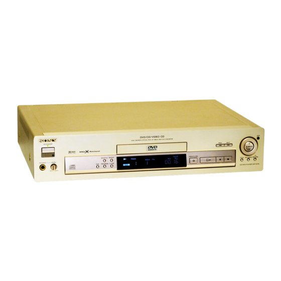
- Page 1 DVP-S715 RMT-D102P SERVICE MANUAL Russian Model SPECIFICATIONS CD/DVD PLAYER MICROFILM...
- Page 2 LINE WITH MARK ! ON THE SCHEMATIC DIAGRAMS AND IN THE PARTS LIST ARE CRITICAL TO SAFE OPERATION. REPLACE THESE COMPONENTS WITH SONY PARTS WHOSE PART NUMBERS APPEAR AS SHOWN IN THIS MANUAL OR IN SUPPLEMENTS PUB- LISHED BY SONY.
-
Page 3: Table Of Contents
TABLE OF CONTENTS Section Title Page Section Title Page Service Note ................4 IC PIN FUNCTION DESCRIPTION GENERAL 5-1. Interface Control Pin Function (MB-78 Board IC604) .. 5-1 System Control Pin Function (MB-78 Board IC805) ..5-2 This Player Can Play the Following Discs ....1-1 Getting Started .............. -
Page 4: Service Note
SERVICE NOTE 1. DISASSEMBLY • This set can be disassembled in the order shown below. Case (Page 2-1) MB-78 Front Panel AU-205 Board Section Board (Page 2-1) (Page 2-1) (Page 2-1) MD Block Ass’y (Page 2-2) TK-47 Tray Board (Page 2-2) (Page 2-2) Optical Skew... - Page 5 2. NOTE ON REMOVE THE CASE 4. HOW TO SERVICE MB-78 BOARD 1) Remove six tapping screws. (See Fig. 1) 1) Remove the case from the set. (Refer to 2-1) 2) Open the side of case. (See Fig. 1) 2) Remove the cover (upper). (Refer to 2-3) 3) Remove the case as lift straight.
- Page 6 5. NOTE ON MOUNTEING SLED MOTOR 1) Push the sled motor ass’y 1 toward direction A. (See Fig. 4) 2) Tighten two screws 2 (M1.7 × 2.5). 1 Sled motor ass’y 2 Two screws (M1.7 × 2.5) Fig. 4 3) Raising the MD block ass’y 3 90 º with the side down. confirm that the optical pick-up 4 falls by self weight.
- Page 7 6. REPLACING OPTICAL PICK-UP 3) In handling the KHS-180A (RP), do not touch inhibited parts shown in Fig. 7, but grip the slide base bearing and U-shaped guide. 6-1. Handling 1) A red laser diode for DVD requires more attention to static Slide base bearing electricity than general infrared laser diodes for CD.
- Page 8 7. NOTE ON ASSEMBLING MECHANICAL DECK 7-1. Application of Grease 1) Grease must be applied if the following parts were replaced. (See Fig. 8) Note 1: Recommended grease is Foil KG-70MP. Note 2: In applying grease, take care not to allow grease to stick to other parts (particularly, rubber belt, spindle motor, and optical pick-up) Base unit holder...
- Page 9 7-2. Cleaning Spindle Motor Turntable 7-4. Deformation of Insulator 1) Remove the tray. (Refer to 2-7) 1) Assemble the spindle base into the base unit. 2) Clean the spindle motor turntable if disc antiskid rubber (black) 2) Lock with 4 shoulder screws. (See Fig. 11) is dirty.
- Page 10 7-6. Note on Mounting TK-47 Board 1) Align two bosses. (See Fig. 13) 2) Align four tabs. (See Fig. 13) 3) Fix the board securely with 3 screws (BV3 × 10). (The sensor will not function normally if the board floats up.) Three screws (BV3 ×...
-
Page 11: General
DVP-S715 SECTION 1 This section is extracted from DVP- GENERAL S715/S315 instruction manual. - Page 20 1-10 E 1-10...
-
Page 21: Disassembly
DVP-S715 SECTION 2 DISASSEMBLY Note: Follow the disassembly procedure in the numerical order given. 2-1. CASE REMOVAL 2-3. MB-78 BOARD REMOVAL 7 Cover (upper) 2 Two tapping screws 5 Two screws 6 Three screws 1 Two tapping screws (B3) (B3) -
Page 22: Md Block Ass'y Removal
2-5. MD BLOCK ASS’Y REMOVAL 2-7. TRAY REMOVAL 1 Two screws 1 Cover (lower) (BVTP3 × 10) 2 Press pully bracket 3 Chassis bracket (B) 2 Two screws (B3) 4 Pull the tray. 6 Remove the tray. 4 Two screws 5 Two screws (B3) (B3) -
Page 23: Sled Motor (M501) Removal
2-9. SLED MOTOR (M501) REMOVAL 2-11. OPTICAL PICK-UP REMOVAL 6 Two screws 4 Optical pick-up (P1.7 × 2.5) 4 Spindle base 5 Screw (PTTWH2 × 5) 3 Main shaft 2 Screw (PTTWH2 × 5) 7 Sled motor (M501) 2 Screw (P2 ×... -
Page 24: Internal Views
2-12. INTERNAL VIEWS Skew motor ass’y (tilt) X-3947-138-1 Optical pick-up Optical pick-up (KHS-180A/J1N) Sled motor ass’y (KHS-180A/J1N) Sled motor ass’y 8-820-005-02 X-3947-137-1 8-820-005-02 X-3947-137-1 DC motor (spindle) 1-698-944-11 Motor (loading) 1-698-942-21 DC motor (spindle) 1-698-944-11... -
Page 25: Circuit Boards Location
2-13. CIRCUIT BOARDS LOCATION POWER BLOCK (HS-930SH) (SWITCHING REGULATOR) FG-43 HP-96 (SLED) (HEAD PHONE) AU-205 (AUDIO) FR-133 (IR/POWER SWITCH) PS-415 (AUDIO POWER) ER-2 (EURO AV) DC MOTOR MB-78 (SPINDLE) (SIGNAL PROCESS/SERVO) TK-47 FL-88 (RF/SERVO) (FL DRIVER/FUNCTION SWITCH) 2-5 E... -
Page 26: Block Diagrams
DVP-S715 SECTION 3 BLOCK DIAGRAMS 3-1. OVERALL BLOCK DIAGRAM AU-205 BOARD MB-78 BOARD (SEE PAGE 4-51) (SEE PAGE 4-17~4-44) SPDIF DIGITAL TK-47 BOARD IC810 IC201, 202 (SEE PAGE 4-7) 4M DRAM 16M SRAM DCRSD IC006 SD0-7 DVD RF IC811 IC204... -
Page 27: Rf/Servo Block Diagram
DVP-S715 3-2. RF/SERVO BLOCK DIAGRAM IC006 ^£ – ^¢ (DVD play) TK-47 BOARD MB-78 BOARD (1/6) (SEE PAGE 4-7) (SEE PAGE 4-25~4-30) IC506 Q009, IC004 RF DET SERVO DSP IC508 800 mVp-p (V) IC501 FILTER HCK/HLDB IC006 COMP DVD RF AMP, SERVO... -
Page 28: Signal Process Block Diagram
DVP-S715 3-3. SIGNAL PROCESS BLOCK DIAGRAM MB-78 BOARD (2/6) (SEE PAGE 4-17, 4-37) IC207 IC201 IC202 24 SCLK 16M SDRAM 16M SDRAM 25 SIN SCLKO R OUT CGCSO G OUT IC810 B OUT I OUT 4M DRAM SYSTEM CONTROL 11 EVEN... -
Page 29: Video Block Diagram
DVP-S715 3-4. VIDEO BLOCK DIAGRAM IC252 %§ IC252 ^¢ IC252 %• IC209 !∞ IC209 !£ IC209 !º 1.1 Vp-p (H) 1.0 Vp-p (H) 0.7 Vp-p (H) 1.1 Vp-p (H) 1.0 Vp-p (H) 0.7 Vp-p (H) MB-78 BOARD (3/6) AU-205 BOARD (1/2) -
Page 30: System Control Block Diagram
DVP-S715 3-5. SYSTEM CONTROL BLOCK DIAGRAM IC807 MB-78 BOARD (4/6) S GATE ARRAY (SEE PAGE 4-17, 4-37, 4-41) IC804 IC802 IC803 L GATE ARRAY 1M SRAM 8M FLASH ı EBSY, ECS, ı HA0-8 IC801 EESI, EWC ı HA0-7, 19-21 HA0-8... -
Page 31: Audio Block Diagram
DVP-S715 3-6. AUDIO BLOCK DIAGRAM AU-205 BOARD (2/2) (SEE PAGE 4-51) PMUTE MODE CONTROL (SEE PAGE 3-13) AUDIO MUTE CN201 (2/2) CN252 (2/2) MAMUTE Q209 J201 MA MUTE IC211 T201 MUTE DRIVE AUDIO MUTE COAXIAL AMUTE SCKG3 SYSTEM CONTROL DIGITAL... -
Page 32: Mode Control Block Diagram
DVP-S715 3-7. MODE CONTROL BLOCK DIAGRAM MB-78 BOARD (6/6) (SEE PAGE 4-34) IC604 IC606 FL-88 BOARD FR-133 BOARD I/F µ-COM COMP. (SEE PAGE 4-54) (SEE PAGE 4-56) ST-BY CONT 1 OUT1 CN601 CN101 CN102 CN401 IC401 REMOTE VIDEO CONTROL VSYNC... -
Page 33: Power Block Diagram
DVP-S715 3-8. POWER BLOCK DIAGRAM TK-47 BOARD MB-78 BOARD (SEE PAGE 4-7) (SEE PAGE 4-17~4-44) CN302 CN008 CN001 S+5V OPTICAL • • DP+5V DEVICE FL008 IC004 IC005 IC006 IC011 A+5V FL005 IC301 IC452 IC455 HS-930SH BOARD IC501 IC502 IC503 PC101... -
Page 34: Frame Schematic Diagram
DVP-S715 4-1. FRAME SCHEMATIC DIAGRAM SECTION 4 PRINTED WIRING BOARDS SCHEMATIC DIAGRAMS THIS NOTE IS COMMON FOR PRINTED WIRING BOARDS AND SCHEMATIC DIAGRAMS. (In addition to this, the necessary mote is printed in each block.) For printed wiring boards: X : indicates a lead wire mounted on the component •... - Page 35 DVP-S715 4-2. PRINTED WIRING BOARDS AND SCHEMATIC DIAGRAMS TK-47 (RF, SERVO) PRINTED WIRING BOARD – Ref. No.: TK-47 board; 3,000 series – TK-47 BOARD CN001 CN002 CN004 CN005 CN008 POWER BLOCK (HS-930SH) D003 (SWITCHING REGULATOR) D004 IC004 FG-43 IC005 HP-96...
- Page 36 There are few cases that the part isn't mounted in this model is printed on this diagram. TK-47 BOARD 1-669-298- (11)
- Page 37 DVP-S715 DVP-S715 TK-47 (RF, SERVO) SCHEMATIC DIAGRAM – Ref. No.: TK-47 board; 3,000 series – • Waveforms 1 IC006 %¡ – %™ (DVD play) 4 IC005 !£ (CD play) 270 mVp-p (V) 500 mV/DIV 1 ms/DIV 2 IC006 ^¡ – ^™ (DVD play) 5 IC005 !∞...
- Page 38 DVP-S715 MB-78 (SIGNAL PROCESS), FG-43 (SLED) PRINTED WIRING BOARDS – Ref. No.: MB-78 board; 1,000 series, FG-43 board; 3,000 series – There are few cases that the part isn't mounted in this model is printed on this diagram. FG-43 MB-78...
-
Page 39: Av Decoder) Schematic Diagram
DVP-S715 MB-78 (AV DECODER) SCHEMATIC DIAGRAM – Ref. No.: MB-78 board; 1,000 series – • Waveforms 1 IC206 8 3.28 Vp-p 27 MHz 2 IC209 1 1.4 Vp-p 27 MHz L64021-A-QC-27 AV DECODER MB-78 (1/8) 4-17 4-18 4-19 4-20... -
Page 40: Video Encoder) Schematic Diagram
DVP-S715 MB-78 (VIDEO ENCODER) SCHEMATIC DIAGRAM • See page 4-12 to 4-16 for printed wiring board. – Ref. No.: MB-78 board; 1,000 series – • Waveforms 1 IC252 &¢ 5 IC252 %• 0.7 Vp-p (H) 0.7 Vp-p (H) 2 IC252 &™... -
Page 41: Drive), Fg-43 (Sled) Schematic Diagrams
DVP-S715 MB-78 (DRIVE), FG-43 (SLED) SCHEMATIC DIAGRAM • See page 4-12 to 4-16 for printed wiring board. – Ref. No.: MB-78 board; 1,000 series, FG-43 board; 3,000 series – • Waveforms 1 IC303 !ª, @™, @£ (DVD play) 5.2 Vp-p 160 Hz 2 IC303 !ª, @™, @£... -
Page 42: Dsp) Schematic Diagram
DVP-S715 MB-78 (DSP) SCHEMATIC DIAGRAM • See page 4-12 to 4-16 for printed wiring board. – Ref. No.: MB-78 board; 1,000 series – • Waveform 1 IC506 ^∞ 3.6 Vp-p 27 MHz MB-78 (4/8) 4-28 4-29 4-30... -
Page 43: Bias) Schematic Diagram
DVP-S715 DVP-S715 MB-78 (BIAS) SCHEMATIC DIAGRAM • See page 4-12 to 4-16 for printed wiring board. – Ref. No.: MB-78 board; 1,000 series – Note: The components identified by mark ! or dotted line with mark ! are critical for safety. -
Page 44: If Μ-Com) Schematic Diagram
DVP-S715 MB-78 (IF µ-COM) SCHEMATIC DIAGRAM • See page 4-12 to 4-16 for printed wiring board. – Ref. No.: MB-78 board; 1,000 series – • Waveform 1 IC604 *™ 5.6 Vp-p 4 MHz IF µ-COM MB-78 (6/8) 4-34 4-35 4-36... -
Page 45: Arp, L Gate Array, Decrypt
DVP-S715 MB-78 (ARP, L GATE ARRAY, DECRYPT) SCHEMATIC DIAGRAM • See page 4-12 to 4-16 for printed wiring board. – Ref. No.: MB-78 board; 1,000 series – • Waveforms 1 IC804 `⁄⁄° 4 IC806 `⁄¤› 225 mVp-p 13.5 MHz 3.0 Vp-p 33 MHz 2 IC804 `⁄⁄fi... -
Page 46: System Μ-Com, S Gate Array
DVP-S715 MB-78 (SYSTEM µ-COM, S GATE ARRAY) SCHEMATIC DIAGRAM • See page 4-12 to 4-16 for printed wiring board. – Ref. No.: MB-78 board; 1,000 series – • Waveform 1 IC805 &£ 4.4 Vp-p 20 MHz SYSTEM µ-COM, S GATE ARRAY... - Page 47 DVP-S715 HP-96 (HEAD PHONE) PRINTED WIRING BOARD AND SCHEMATIC DIAGRAM – Ref. No.: HP-96 board; 4,000 series – There are few cases that the part isn't mounted in this model is printed on this diagram. HP-96 HP-96 BOARD(SIDE B) BOARD(SIDE A)
- Page 48 DVP-S715 AU-205 (AUDIO) SCHEMATIC DIAGRAM – Ref. No.: AU-205 board; 2,000 series – • Waveforms 1 IC209 !∞ 1.1Vp-p (H) 2 IC209 !£ 1.0 Vp-p (H) 3 IC209 0 0.7 Vp-p (H) AUDIO AU-205 4-51 4-52 4-53...
- Page 49 DVP-S715 FL-88 (FL DRIVER, FUNCTION SWITCH), FR-133 (IR, POWER SWITCH) SCHEMATIC DIAGRAMS – Ref. No.: FL-88 board; 2,000 series, FR-133 board; 2,000 series – FL DRIVER/FUNCTION SW, IR/POWER SW FL-88, FR-133 4-54 4-55 4-56...
- Page 50 DVP-S715 FL-88 (FL DRIVER, FUNCTION SWITCH), FR-133 (IR, POWER SWITCH) PRINTED WIRING BOARDS There are few cases that the part isn't mounted in this model is printed on this diagram. – Ref. No.: FL-88 board; 2,000 series, FR-133 board; 2,000 series –...
- Page 51 DVP-S715 ER-2 (EURO AV) SCHEMATIC DIAGRAM – Ref. No.: ER-2 board; 2,000 series – EURO AV ER-2 4-61 4-62 4-63 4-64...
- Page 52 DVP-S715 ER-2 (EURO AV) PRINTED WIRING BOARD – Ref. No.: ER-2 board; 2,000 series – There are few cases that the part isn't mounted in this model is printed on this diagram. ER-2 BOARD(SIDE B) EURO AV(LINE 1) EURO AV(LINE 2)
- Page 53 DVP-S715 DVP-S715 PS-415 (AUDIO POWER) PRINTED WIRING BOARD AND SCHEMATIC DIAGRAM – Ref. No.: PS-415 board; 2,000 series – There are few cases that the part isn't mounted in this model is printed on this diagram. POWER BLOCK (HS-930SH) (SWITCHING REGULATOR)
- Page 54 DVP-S715 POWER BLOCK (HS-930SH) (POWER) PRINTED WIRING BOARD AND SCHEMATIC DIAGRAM – Ref. No.: POWER BLOCK (HS-930SH board); 4,000 series – There are few cases that the part isn't mounted in this model is printed on this diagram. HS-930SH BOARD...
-
Page 55: Interface Control Pin Function (Mb-78 Board Ic604)
5-1. INTERFACE CONTROL PIN FUNCTION (IC604 on MB-78 Board (6/8)) Pin No. Pin Name Function Pin No. Pin Name Function A16-19 Set Address 40, 41 AD2, 3 Input of AD 5, 6 TIN0, 1 – Not used – 7, 8 TOT0, 1 –... - Page 56 5-2. SYSTEM CONTROL PIN FUNCTION (IC805 on MB-78 Board (8/8)) Pin No. Pin Name Function Pin No. Pin Name Function PB14/IRQ6 Input of interrupt fromIC506 IRQ0 Input of interrupt fromIC203 PB15/IRQ7 Input of interrupt fromIC804 IRQ1 Input of DMA request from IC203 –...
- Page 57 Pin No. Pin Name Function – Not used – Not used – Not used – Not used – Not used – Digital ground RxD0 Input of serial data TxD0 Output of serial data RxD1 Input of serial data TxD1 Output of serial data SCK0 Output of serial clock SCK1...
-
Page 58: Test Mode
6-1. Starting up Test Mode Syscon Diagnosis IF con Ver. 0.620 (9315) With the DVP-S715 turned off, press [TITLE], [CLEAR], and SYScon Ver. 0.400 (0000) [POWER] keys on the Remocon in this order, and the Test mode →Enter item No.[02] ;... -
Page 59: Error Display
6-3. Error Display (3) Destination Setting (3-2) Destination setting Check In case of an error, the error code and information are displayed as shown in Figure 7. I/O port read Syscon Diagnosis Error:Not detected IF con Ver. 0.620 (9315) SYScon Ver. 0.400 (62ED) →Check item name RAM Check The destination setting port (I/O) is read, and displayed with hex. - Page 60 (5-4) Servo DSP Download (6) Data Source DSP (IC506) code area ROM/RAM discrimination (6-2) Register in ARP (IC806) RAM: Program download → Revision data read Register write → Register read matching check ROM: Revision data read Error 04: Data read error Error 05: Write/read data mismatch error 13: DSP data not ready Data from “0x00”...
- Page 61 (6-6) Register in Decrypt IC (IC811) (7-3) Reset Line in AV Decoder (IC203) Register write → Register read matching check Register write → Hard reset → Register read matching check Error 05: Write/read data mismatch error Error 02: Reset error 05: Write/read data mismatch error 0x00 –...
- Page 62 (7-6) Connection from ARP (IC806) to AV Decoder (IC203) (8-4) 1914 Vsync ROM data → ARP (IC806) → Decrypt (IC811) → AV Decoder CPU measures the 1914 Vsync interrupt cycle. (IC203) Error 41: Vsync interruption is not detected Error 04: Data read error 42: Vsync interrupt cycle error 05: Write/read data mismatch error 06: DMA transfer DREQ error...
- Page 63 (8-8) S Terminal DC Check (8-13) AV CONT Through Check Color bar output by Video Encoder (IC252) Color bar output by video encoder Error 11: Serial transfer error Error 11: Serial transfer error The color bars are output in the same manner as in (8-2). Input picture is sent as it is from EURO AV2 (CNJ601) to the AV1 After VS signal is turned on/off repeatedly two times, the color (CNJ602).
- Page 64 (9-5) Audio Digital Output (9-8) Dual DAC (Serial) ROM audio data → ARP (IC806) → AV Decoder (IC203) → Digi- ROM audio data → ARP (IC806) → AV Decoder (IC203) → 2ch DAC (IC215) → Analog audio output (Attenuation) tal audio I/F output Error 10: ARP (IC806) →...
- Page 65 g Error Codes in Diagnostic Test 01: Mode not supported is selected 02: Reset error 03: Data write error 04: Data read error 05: Write/read data mismatch error 06: DMA transfer DREQ error 07: DMA transfer address error 10: Chip-to-chip data transfer error 11: Serial transfer error 12: EEPROM is not ready 13: DSP data is not ready...
-
Page 66: Drive Auto Adjustment
6-5. Drive Auto Adjustment The tray opens after the [ENTER] key is pressed and the initial- ization is finished. Then, place the DVD_SL disc for adjustment. Press the [ENTER] key to start adjustment. During adjustment, The drive can be automatically adjusted, except disc change and the tangential skew adjustment screen is displayed. - Page 67 Drive Automatic Adjustment Flowchart DVD_SL Loading adjustment Adj. disc selection FOK Check STOP Tracking ON Select “ALL” Sled ON AGC ON CLVA EEPROM Default Set Lock Check STOP Hydet Init Sled Init Go To Home Position Auto Loop Filter Offset Auto Focus Offset Auto Tilt Offset Auto Focus Offset...
- Page 68 DVD_SL adjustment adjustment Auto Loop Filter Offset FOK Check STOP Auto Focus Offset Auto Tilt Offset Auto Focus Offset Auto Focus Gain Auto Tracking Offset Auto Tracking Gain Auto EQ. Auto Loop Filter Offset Pull in Memory FOK Check STOP Jitter Check Tracking ON Sled ON...
- Page 69 DVD_DL DVD_DL adjustment adjustment Disc Type Check FOK Check STOP Tracking ON LD ON Sled ON Spindle start CLVA Tilt ON Focus ON Lock Check FOK Check STOP Layer Check STOP sled move Auto Focus Offset Auto Tracking Offset Auto Tilt Offset Auto Focus Offset Auto Focus Gain Auto Tracking Gain...
-
Page 70: Drive Manual Operation
6-6. Drive Manual Operation 6-6-3. Manual Control 1 Manual Control 1 In performing manual operation, observe the following points: Select correct disc type on the Disc Type screen. SA.000000 SI.00 EMG.00 First, select “0. Disc Type” and execute “7. Hydet init” and “8. Sled init”. -
Page 71: Manual Control 2
6-6-4. Manual Control 2 6-6-6. Manual Adjust 1 Manual Control 2 Manual Adjust 1 SA.000000 SI.00 EMG.00 SA.000000 SI.CD EMG.00 0. Pause 4. Eject 0. TRK. Off set 1. FCS. Srch 5. Load 1. TRK. Off set 2 (DVD) 3. Tilt_H 2. -
Page 72: Manual Adjust 2
6-6-7. Manual Adjust 2 3. Auto Focus Gain : Adjust focus gain automatically. Adjusted result is reflected on the EEPROM. Execute this with CLVA turned on if possible. If Manual Adjust 2 NG, the system will be defective, and re- SA.000000 SI.00 EMG.00... -
Page 73: Eeprom Data Screen Display
6-6-10. EEPROM data screen display EEPROM data Focus Offset Focus Gain TRK Offset TRK. CONT. TRK Gain Tilt Offset Pullin Level EQ. Boost L.F.O SD. ?? HY. ?? Figure 20 This screen displays various set values including adjusted results stored in the EEPROM. ID No. -
Page 74: Emergency History
6-8. Emergency History EMG Hist Page 4 000000 Hour With the initial menu displayed, press [4] key on the standard com- N Emergency history (7) 00 00 00 00 00 00 mander, and the information on emergency history of Drvcon and 00 00 00 00 00 00 Syscon will be displayed. - Page 75 How to see Emergency History Recovery NG Auto Sequence Time Out Auto Sequence Fail Syscon Stop request from drive controller was received At the mode change command, the mode could not be changed within specified time and the 1 EMG CODE drive stopped.
-
Page 76: Error Code
3 Disc Type (Mecha Mode: 6π) 6-9. Error Code The self-diagnosis function works to prevent the player from mal- functioning, a five-digit service number (combination of a letter and figures) flashes on the screen and front panel display. 1. Each user needs to manage the error......“C” code (A) Last result of disc type judgment. - Page 77 2. Each user needs to contact Code Description with the service section ..........“E” code At the mode change command, the mode could not be changed within specified time and the drive stopped. Retry due to supply error failed and the drive stopped.
-
Page 78: Electrical Adjustment
DVP-S715 SECTION 7 ELECTRICAL ADJUSTMENT 7-1. Power Supply Check In making adjustment, refer to 7-4. Adjustment Related Parts Arrangement. 1. HS-930SH Board Note: During diagnostic check, the characters and color bars can Mode be seen only with the NTSC monitor. Therefore, for diag-... -
Page 79: Adjustment Of System Control
7-2. Adjustment of System Control 2. S-terminal Output Check (MB-78 board) <Purpose> Check S-terminal video output. If it is incorrect, pictures will not 1. System Clock 27 MHz Adjustment (MB-78 board) be displayed correctly in spite of connection to the TV with an S- <Purpose>... -
Page 80: Checking S Video Output S-C
4. Checking Component Video Output R-Y 6. Checking S Video Output S-C (MB-78 board) (MB-78 board) <Purpose> <Purpose> This checks whether the S-C satisfies the NTSC Standard. If it is This checks component video output R-Y. If it is incorrect, cor- not correct, the colors will be too dark or light. -
Page 81: Adjustment Related Parts Arrangement
7-4. Adjustment Related Parts Arrangement MB-78 BOARD (Side A) CN251 RV251 VIDEO LEVEL IC206 CT201 SYS CLK (27 MHz) ADJ MB-78 BOARD (Side B) CN252 HS-930SH BOARD (Side A) CN201 11 12 7-4 E... -
Page 82: Repair Parts List
DVP-S715 SECTION 8 REPAIR PARTS LIST 8-1. EXPLODED VIEWS The components identified by mark ! or dotted line with mark ! are criti- cal for safety. NOTE: Replace only with part number speci- • The mechanical parts with no reference number in •... -
Page 83: Front Panel Assembly
X-3948-385-1 PANEL ASSY, FRONT * 61 A-6065-074-A FR-133 BOARD, COMPLETE 3-988-036-01 WINDOW, INDICATION * 62 1-500-544-11 BEAD, FERRITE 4-942-568-01 EMBLEM (NO.5), SONY 1-783-345-11 CABLE, FLEXIBLE FLAT (FML-5) (20P) 3-988-031-01 BUTTON, OPEN A-6065-112-A FL-88 BOARD, COMPLETE 3-945-284-51 KNOB, VOLUME 1-475-685-11 ENCODER, ROTARY... -
Page 84: Chassis Assembly
8-1-3. CHASSIS ASSEMBLY supplied supplied supplied supplied supplied supplied supplied supplied The components identified by mark T901 ! or dotted line with mark ! are criti- supplied cal for safety. supplied Replace only with part number speci- supplied fied. Ref. No. Part No. -
Page 85: Dvd Mechanism Chassis Assembly (1)
8-1-4. DVD MECHANISM CHASSIS ASSEMBLY (1) supplied M902 Ref. No. Part No. Description Remark Ref. No. Part No. Description Remark 3-973-099-01 TRAY (B) 3-975-089-01 BRACKET, PRESS PULLEY 3-975-073-02 GEAR, CAM * 161 3-975-074-01 PULLEY, PRESS 3-975-087-01 GEAR, DRIVE 3-975-077-01 SCREW, BU STOPPER 3-975-086-01 GEAR, TRAY DRIVING * 163 3-975-088-01 HOLDER, BASE UNIT... -
Page 86: Dvd Mechanism Chassis Assembly (2)
8-1-5. DVD MECHANISM CHASSIS ASSEMBLY (2) M501 M903 M901 The components identified by mark ! or dotted line with mark ! are criti- cal for safety. Replace only with part number speci- fied. Ref. No. Part No. Description Remark Ref. No. Part No. -
Page 87: Electrical Parts List
AU-205 8-2. ELECTRICAL PARTS LIST NOTE: The components identified by • Due to standardization, replacements in the • Items marked “*” are not stocked since they mark ! or dotted line with mark parts list may be different from the parts speci- are seldom required for routine service. - Page 88 AU-205 Ref. No. Part No. Description Remark Ref. No. Part No. Description Remark FB203 1-414-553-11 FERRITE Q202 8-729-141-58 TRANSISTOR 2SC2275A-QP FB204 1-414-135-11 FERRITE Q203 8-729-231-55 TRANSISTOR 2SC2878-AB FB205 1-414-135-11 FERRITE Q204 8-729-231-55 TRANSISTOR 2SC2878-AB Q205 8-729-424-18 TRANSISTOR UN2113 FB206 1-414-135-11 FERRITE FB207 1-414-135-11 FERRITE Q206...
- Page 89 AU-205 ER-2 Ref. No. Part No. Description Remark Ref. No. Part No. Description Remark R251 1-216-065-91 RES,CHIP 4.7K 1/10W C632 1-164-004-11 CERAMIC CHIP 0.1uF R252 1-216-025-91 RES,CHIP 1/10W C633 1-164-004-11 CERAMIC CHIP 0.1uF R253 1-249-883-11 CARBON 1/4W C634 1-164-004-11 CERAMIC CHIP 0.1uF R254 1-249-883-11 CARBON...
- Page 90 ER-2 Ref. No. Part No. Description Remark Ref. No. Part No. Description Remark D613 8-719-067-40 DIODE STZ6.8N-T146 Q607 8-729-023-22 TRANSISTOR 2SD2114KT146 D614 8-719-067-40 DIODE STZ6.8N-T146 Q608 8-729-023-22 TRANSISTOR 2SD2114KT146 D615 8-719-067-40 DIODE STZ6.8N-T146 Q612 8-729-424-56 TRANSISTOR UN211L Q614 8-729-023-22 TRANSISTOR 2SD2114KT146 D616 8-719-067-40 DIODE STZ6.8N-T146 Q615...
- Page 91 ER-2 FG-43 FL-88 Ref. No. Part No. Description Remark Ref. No. Part No. Description Remark R638 1-216-113-00 METAL CHIP 470K 1/10W R750 1-216-037-00 METAL CHIP 1/10W R639 1-216-113-00 METAL CHIP 470K 1/10W R753 1-216-049-91 RES,CHIP 1/10W R640 1-216-041-00 METAL CHIP 1/10W R754 1-216-089-91 RES,CHIP...
- Page 92 FL-88 FR-133 HP-96 Ref. No. Part No. Description Remark Ref. No. Part No. Description Remark < IC > < SWITCH > IC101 8-759-438-82 IC uPD16311GC-AB6 S105 1-771-349-21 SWITCH, KEYBOARD (CLEAR) S106 1-771-349-21 SWITCH, KEYBOARD (REPEAT) < COIL > S107 1-771-349-21 SWITCH, KEYBOARD (PROGRAM) S108 1-771-349-21 SWITCH, KEYBOARD (SHUFFLE) L101...
- Page 93 HP-96 MB-78 Ref. No. Part No. Description Remark Ref. No. Part No. Description Remark C008 1-163-021-91 CERAMIC CHIP 0.01uF C011 1-126-206-11 ELECT CHIP 100uF 6.3V C009 1-163-021-91 CERAMIC CHIP 0.01uF C012 1-126-206-11 ELECT CHIP 100uF 6.3V < CONNECTOR > C015 1-126-204-11 ELECT CHIP 47uF C016...
- Page 94 MB-78 Ref. No. Part No. Description Remark Ref. No. Part No. Description Remark C264 1-107-826-11 CERAMIC CHIP 0.1uF C378 1-107-826-11 CERAMIC CHIP 0.1uF C379 1-107-826-11 CERAMIC CHIP 0.1uF C265 1-162-970-11 CERAMIC CHIP 0.01uF C380 1-107-826-11 CERAMIC CHIP 0.1uF C266 1-162-970-11 CERAMIC CHIP 0.01uF C381 1-107-826-11 CERAMIC CHIP...
- Page 95 MB-78 Ref. No. Part No. Description Remark Ref. No. Part No. Description Remark C546 1-162-970-11 CERAMIC CHIP 0.01uF C824 1-162-970-11 CERAMIC CHIP 0.01uF C547 1-162-970-11 CERAMIC CHIP 0.01uF C825 1-162-970-11 CERAMIC CHIP 0.01uF C548 1-128-004-11 ELECT CHIP 10uF C826 1-162-970-11 CERAMIC CHIP 0.01uF C549 1-107-826-11 CERAMIC CHIP...
- Page 96 MB-78 Ref. No. Part No. Description Remark Ref. No. Part No. Description Remark < DIODE > FL008 1-233-893-21 FILTER, CHIP EMI FL201 1-233-893-21 FILTER, CHIP EMI D002 8-719-975-40 DIODE RB411D FL202 1-233-893-21 FILTER, CHIP EMI D101 8-719-988-62 DIODE 1SS355 D102 8-719-988-62 DIODE 1SS355 FL204 1-239-400-11 FILTER, CHIP EMI...
- Page 97 MB-78 Ref. No. Part No. Description Remark Ref. No. Part No. Description Remark IC606 8-759-100-93 IC uPC393G2 R156 1-216-864-11 METAL CHIP 1/16W R157 1-216-864-11 METAL CHIP 1/16W IC801 8-759-431-99 IC BR9020F-E2 IC802 8-759-526-77 IC HM628128ALFP-5SL R158 1-216-864-11 METAL CHIP 1/16W IC803 8-759-546-58 IC MBM29F800BA-90PF R159...
- Page 98 MB-78 Ref. No. Part No. Description Remark Ref. No. Part No. Description Remark R232 1-216-845-11 METAL CHIP 100K 1/16W R314 1-216-821-11 METAL CHIP 1/16W R235 1-216-864-11 METAL CHIP 1/16W R315 1-216-837-11 METAL CHIP 1/16W R236 1-216-809-11 METAL CHIP 1/16W R316 1-216-818-11 METAL CHIP 1/16W R237...
- Page 99 MB-78 Ref. No. Part No. Description Remark Ref. No. Part No. Description Remark R388 1-216-864-11 METAL CHIP 1/16W R518 1-216-864-11 METAL CHIP 1/16W R393 1-216-797-11 METAL CHIP 1/16W R519 1-216-825-11 METAL CHIP 2.2K 1/16W R394 1-216-797-11 METAL CHIP 1/16W R520 1-216-825-11 METAL CHIP 2.2K 1/16W...
- Page 100 MB-78 Ref. No. Part No. Description Remark Ref. No. Part No. Description Remark R585 1-216-821-11 METAL CHIP 1/16W R677 1-216-809-11 METAL CHIP 1/16W R586 1-216-833-11 METAL CHIP 1/16W R678 1-216-809-11 METAL CHIP 1/16W R587 1-216-809-11 METAL CHIP 1/16W R588 1-216-809-11 METAL CHIP 1/16W R679 1-216-809-11 METAL CHIP...
- Page 101 MB-78 POWER (HS-930SH) Ref. No. Part No. Description Remark Ref. No. Part No. Description Remark R852 1-218-871-11 RES,CHIP 0.50% 1/16W < VIBRATOR > R853 1-218-871-11 RES,CHIP 0.50% 1/16W X201 1-767-990-11 VIBRATOR, CRYSTAL (27MHz) R854 1-216-809-11 METAL CHIP 1/16W X601 1-767-359-11 VIBRATOR, CERAMIC (4MHz) R855 1-216-833-11 METAL CHIP 1/16W...
- Page 102 POWER (HS-930SH) PS-415 TK-47 Ref. No. Part No. Description Remark Ref. No. Part No. Description Remark < PHOTO COUPLER > FL952 1-233-893-21 FILTER, CHIP EMI FL953 1-233-893-21 FILTER, CHIP EMI ! PC101 8-749-010-59 PHOTO COUPLER TLP721F < IC > < TRANSISTOR > IC951 8-759-231-58 IC M5F7812L Q101...
- Page 103 TK-47 Ref. No. Part No. Description Remark Ref. No. Part No. Description Remark < TRANSISTOR > C061 1-163-989-11 CERAMIC CHIP 0.033uF C062 1-124-779-00 ELECT CHIP 10uF Q001 8-729-420-24 TRANSISTOR 2SB1218A-QRS C064 1-124-779-00 ELECT CHIP 10uF Q004 8-729-805-25 TRANSISTOR 2SB1121 C065 1-109-982-11 CERAMIC CHIP Q005 8-729-805-25 TRANSISTOR 2SB1121...
- Page 104 TK-47 Ref. No. Part No. Description Remark Ref. No. Part No. Description Remark R161 1-216-097-91 RES,CHIP 100K 1/10W R162 1-216-077-00 METAL CHIP 1/10W R163 1-216-081-00 METAL CHIP 1/10W R164 1-216-295-91 SHORT R165 1-216-295-91 SHORT R166 1-216-065-91 RES,CHIP 4.7K 1/10W R167 1-216-065-91 RES,CHIP 4.7K 1/10W...
Need help?
Do you have a question about the DVP-S715 and is the answer not in the manual?
Questions and answers