Table of Contents
Advertisement
Quick Links
Advertisement
Chapters
Table of Contents

Related Manuals for Clevo M720SR


Summary of Contents for Clevo M720SR
- Page 3 Preface Notebook Computer M72XSR Service Manual...
- Page 4 Preface Notice The company reserves the right to revise this publication or to change its contents without notice. Information contained herein is for reference only and does not constitute a commitment on the part of the manufacturer or any subsequent ven- dor.
- Page 5 Preface About this Manual This manual is intended for service personnel who have completed sufficient training to undertake the maintenance and inspection of personal computers. It is organized to allow you to look up basic information for servicing and/or upgrading components of the M72XSR series notebook PC.
- Page 6 Preface IMPORTANT SAFETY INSTRUCTIONS Follow basic safety precautions, including those listed below, to reduce the risk of fire, electric shock and injury to per- sons when using any electrical equipment: 1. Do not use this product near water, for example near a bath tub, wash bowl, kitchen sink or laundry tub, in a wet basement or near a swimming pool.
-
Page 7: Instructions For Care And Operation
Preface Instructions for Care and Operation The notebook computer is quite rugged, but it can be damaged. To prevent this, follow these suggestions: Don’t drop it, or expose it to shock. If the computer falls, the case and the components could be damaged. Do not expose the computer Do not place it on an unstable Do not place anything heavy... -
Page 8: Power Safety
Preface Avoid interference. Keep the computer away from high capacity transformers, electric motors, and other strong mag- netic fields. These can hinder proper performance and damage your data. Take care when using peripheral devices. Use only approved brands of Unplug the power cord before peripherals. -
Page 9: Battery Precautions
Preface Battery Precautions • Only use batteries designed for this computer. The wrong battery type may explode, leak or damage the computer. • Do not continue to use a battery that has been dropped, or that appears damaged (e.g. bent or twisted) in any way. Even if the computer continues to work with a damaged battery in place, it may cause circuit damage, which may possibly result in fire. - Page 10 Preface Related Documents You may also need to consult the following manual for additional information: User’s Manual on CD This describes the notebook PC’s features and the procedures for operating the computer and its ROM-based setup pro- gram. It also describes the installation and operation of the utility programs provided with the notebook PC. VIII...
-
Page 11: Table Of Contents
Preface Contents Introduction ..........1-1 Top without Fingerprint (M720SR) ..........A-4 Top with Fingerprint (M725SR) ............ A-5 Overview ..................1-1 Top without Fingerprint (M725SR) ..........A-6 System Specifications ..............1-2 Bottom (M72XSR) ................ A-7 Model Differences ................1-5 LCD (M720SR) ................A-8 External Locator - Top View with LCD Panel Open ......1-6 LCD (M725SR) ................ - Page 12 Preface ENE MR510, 7 IN 1 ..............B-23 SATA, 3G POWER, PCI DEBUG ..........B-24 AUDIO CODEC ALC883 ............B-25 AUDIO AMP ................B-26 KBC-ITE IT8512E ............... B-27 SYSTEM POWER ..............B-28 VCORE ..................B-29 VDD3, VDD5 ................B-30 1.05VS, 1.2V, 1.5V ..............B-31 1.8V, 0.9VS ..................
-
Page 13: Introduction
Introduction Chapter 1: Introduction Overview This manual covers the information you need to service or upgrade the M72XSR series notebook computer. Information about operating the computer (e.g. getting started, and the Setup utility) is in the User’s Manual. Information about driv- ers (e.g. -
Page 14: System Specifications
Introduction System Specifications Latest Specification Information The specifications listed in this Appendix are correct at the time of going to press. Certain items (particularly processor types/speeds and CD/DVD device types) may be changed, delayed or updated due to the manufacturer's release schedule. Check with your service center for details. - Page 15 Introduction Feature Specification Storage One Changeable 12.7mm(h) Optical Device (CD/DVD) Type Drive (see “Optional” on page 1 - 4 for drive options) Easy Changeable 2.5" 9.5 mm (h) SATA (Serial) HDD Audio Intel High Definition Audio Compliant Interface A3D™ Compatible Compliant with Microsoft UAA (Universal Audio Architecture) S/PDIF Digital Output Direct Sound 3D™...
- Page 16 Introduction Feature Specification Environmental Temperature Relative Humidity ° ° Spec Operating: C - 35 Operating: 20% - 80% Non-Operating: -20°C - 60°C Non-Operating: 10% - 90% Dimensions 299mm (w) * 219mm (d) * 26.5 - 35.7mm (h) 1.8 kg With 4 Cell Battery &...
-
Page 17: Model Differences
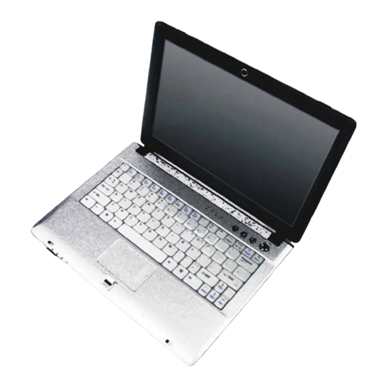
Introduction Model Differences The models vary slightly in external cover design and color. Figure 1 Model Differences System Specifications 1 - 5... -
Page 18: External Locator - Top View With Lcd Panel Open
Introduction External Locator - Top View with LCD Panel Open Figure 2 Top View 1. Built-In PC Camera (Optional) 2. LCD 3. Speakers 4. Power Button 5. Hot-Key Buttons 6. LED Status Indicators 7. Keyboard 8. Touchpad & Buttons 9. LED Power & Communication Indicators 10. -
Page 19: External Locator - Front & Rear Views
Introduction External Locator - Front & Rear Views Figure 3 Front View 1. LCD Latches 2. LED Power & Communication Indicators 3. 7-in-1 Card Reader 4. S/PDIF-Out Jack Front 5. Microphone-In Jack 6. Headphone-Out Jack Figure 4 Rear View 1. Battery Rear External Locator - Front &... -
Page 20: External Locator - Left & Right Side Views
Introduction External Locator - Left & Right Side Views Figure 5 Left Side View 1. DC-In Jack 2. RJ-45 LAN Jack 3. External Monitor Port 4. Vent Left 5. 2 * USB 2.0 Ports 6. ExpressCard/ 54(34) Slot Figure 6 Right Side View 1. -
Page 21: External Locator - Bottom View
Introduction External Locator - Bottom View Figure 7 Bottom View 1. Battery 2. Hard Disk Bay Cover (3.5G Module) 3. RAM & CPU Bay Cover Overheating To prevent your com- puter from overheating make sure nothing blocks the vent/fan in- takes while the com- puter is in use. -
Page 22: Mainboard Overview - Top (Key Parts)
Introduction Mainboard Overview - Top (Key Parts) Figure 8 Mainboard Top Key Parts 1. Clock Buffer ICS9P935 2. ITE 8512E 3. ExpressCard Assembly 1 - 10 Mainboard Overview - Top (Key Parts) -
Page 23: Mainboard Overview - Bottom (Key Parts)
Introduction Mainboard Overview - Bottom (Key Parts) Figure 9 Mainboard Bottom Key Parts 1. CPU Socket (no CPU installed) 2. LAN PHY RTL8201CL 3. CLOCK GENERATOR ICS9LPR600 4. Northbridge- SiSM672 5. 7-in-1 Card Reader Controller 6. Card Reader Controller ENE MR510 7. -
Page 24: Mainboard Overview - Top (Connectors)
Introduction Mainboard Overview - Top (Connectors) Figure 10 Mainboard Top Connectors 1. External Monitor Port 2. RJ-45 LAN Jack 3. CCD Cable Connector 4. LCD Cable Connector 5. Speaker Cable Connector 6. Touch Pad Cable Connector 7. Fingerprint Cable Connector 8. -
Page 25: Mainboard Overview - Bottom (Connectors)
Introduction Mainboard Overview - Bottom (Connectors) Figure 11 Mainboard Bottom Connectors 1. DC-In Jack 2. RJ-45 LAN Jack 3. External Monitor Port 4. Inverter Cable Connector 5. USB Port 6. S/PDIF-Out Jack 7. Microphone-In Jack 8. Headphone-Out Jack 9. Optical Device Drive Connector 10. - Page 26 Introduction 1 - 14...
-
Page 27: Disassembly
Disassembly Chapter 2: Disassembly Overview This chapter provides step-by-step instructions for disassembling the M72XSR series notebook’s parts and subsystems. When it comes to reassembly, reverse the procedures (unless otherwise indicated). We suggest you completely review any procedure before you take the computer apart. Procedures such as upgrading/replacing the RAM, CD device and hard disk are included in the User’s Manual but are repeated here for your convenience. -
Page 28: Maintenance Tools
Disassembly NOTE: All disassembly procedures assume that the system is turned OFF, and disconnected from any power supply (the battery is removed too). Maintenance Tools The following tools are recommended when working on the notebook PC: • M3 Philips-head screwdriver •... -
Page 29: Maintenance Precautions
Disassembly Maintenance Precautions The following precautions are a reminder. To avoid personal injury or damage to the computer while performing a re- moval and/or replacement job, take the following precautions: Power Safety Warning 1. Don't drop it. Perform your repairs and/or upgrades on a stable surface. If the computer falls, the case and other Before you undertake components could be damaged. -
Page 30: Remove The Battery
Disassembly Disassembly Steps The following table lists the disassembly steps, and on which page to find the related information. PLEASE PERFORM THE DISASSEMBLY STEPS IN THE ORDER INDICATED. To remove the Battery: To remove the Optical Device: 1. Remove the battery page 2 - 5 1. -
Page 31: Removing The Battery
Disassembly Removing the Battery Figure 1 1. Turn the computer off, and turn it over. Battery Removal 2. Slide the latches ( & ) the direction of the arrow, and hold latch in place. 3. Slide the battery in the direction of the arrow a. -
Page 32: Removing The Hard Disk Drive
Disassembly Removing the Hard Disk Drive The hard disk drive can be taken out to accommodate other 2.5" serial (SATA) hard disk drives with a height of 9.5mm Figure 2 (h). Follow your operating system’s installation instructions, and install all necessary drivers and utilities (as outlined in HDD Assembly Chapter 4 of the User’s Manual) when setting up a new hard disk. - Page 33 Disassembly 4. Carefully grip the mylar cover tab and slide the hard disk in the direction of arrow. Figure 3 5. Lift the hard disk up Figure d in the direction of arrow. HDD Assembly 6. Remove the screws and separate the mylar cover from the hard disk Sequence Removal...
-
Page 34: Removing The System Memory (Ram)
Disassembly Removing the System Memory (RAM) Figure 4 RAM Module The computer has two memory sockets for 200 pin Small Outline Dual In-line Memory Modules (SO-DIMM) supporting Removal DDRII 533/667MHz. The main memory can be expanded up to 2GB. The SO-DIMM modules supported are 256MB, 512MB and 1024MB DDRII Modules. -
Page 35: Remove The Battery
Disassembly 7. Gently push the two release latches ( & on the sides of the memory socket in the direction indicated by the Figure 5 arrows (Figure Memory Removal 8. The RAM module(s) will pop-up Figure e , and you can then remove it. Sequence d. -
Page 36: Removing The Processor
Disassembly Removing the Processor Figure 6 Processor Removal 1. Turn off the computer, and remove the battery (page 2 - 6) and the CPU/RAM bay cover (page 2 - 2. The CPU heat sink will be visible at point on the mainboard. a. - Page 37 Disassembly 5. Turn the release latch towards the unlock symbol , to release the CPU (Figure Figure 7 6. Carefully (it may be hot) lift the CPU up out of the socket (Figure Processor Removal 7. Reverse the process to install a new CPU. Sequence 8.
-
Page 38: Removing The Wireless Lan Module
Disassembly Removing the Wireless LAN Module Figure 8 Wireless LAN 1. Turn off the computer, remove the battery (page 2 - 6) and the CPU/RAM bay cover (page 2 - Module Removal 2. The Wireless LAN module will be visible at point on the mainboard. -
Page 39: Removing The Bluetooth Module
Disassembly Removing the Bluetooth Module Figure 9 Bluetooth Removal 1. Turn off the computer, remove the battery (page 2 - 6), and the CPU/RAM bay cover (page 2 - 2. The Bluetooth will be visible at point on the mainboard. a. -
Page 40: Removing The Optical (Cd/Dvd) Device
Disassembly Removing the Optical (CD/DVD) Device Figure 10 Optical Device 1. Turn off the computer, remove the battery (page 2 - 6), and the CPU/RAM bay cover (page 2 - Removal 2. Remove the screw at point , and use a screwdriver to carefully push out the optical device at point 3. -
Page 41: Removing The Keyboard
Disassembly Removing the Keyboard Figure 11 Keyboard Removal 1. Turn off the computer, and remove the battery (page 2 - 2. Press the three keyboard latches at the top of the keyboard to elevate the keyboard from its normal position (you a. -
Page 42: Removing The Modem Module
Disassembly Removing the Modem Module Figure 12 Modem Removal 1. Turn off the computer, remove the battery (page 2 - 6) and the CPU/RAM bay cover (page 2 - 8) and the CPU heat sink (page 2 - 6) and the Wireless LAN and the optical device (page 2 - 8) and the keyboard (page 2 -... - Page 43 Disassembly 6. Remove screws and disconnect the connectors from the mainboard. Figure 13 7. Separate the bottom case from the mainboard and turn it over. Modem Removal 8. Remove the screws and disconnect the connector from the modem. Sequence 9. Lift the modem up off the socket e.
- Page 44 Disassembly 2 - 18...
-
Page 45: Part Lists
Part Lists Appendix A:Part Lists This appendix breaks down the M72XSR series notebook’s construction into a series of illustrations. The component part numbers are indicated in the tables opposite the drawings. Note: This section indicates the manufacturer’s part numbers. Your organization may use a different system, so be sure to cross-check any relevant documentation. -
Page 46: Part List Illustration Location
Table A - 1 Part List Illustration Part Pages# Location page A - 3 Top with Fingerprint - (M720SR) page A - 4 Top without Fingerprint - (M720SR) page A - 5 Top with Fingerprint - (M725SR) page A - 6... -
Page 47: Top With Fingerprint (M720Sr
Top with Finger- print (M720SR) 黑色 無鉛 白色 無鉛 無鉛 無鉛 無鉛 無鉛 無鉛 (設變) 無鉛 (設變) 無鉛 (設變) 無鉛 無鉛 無鉛 無鉛 無鉛 無鉛 無鉛 無鉛 無鉛 無鉛 無鉛 無鉛 無鉛 無鉛 無鉛 無鉛 Top with Fingerprint (M720SR) A - 3... -
Page 48: Top Without Fingerprint (M720Sr
Top without Fin- gerprint (M720SR) 黑色 無鉛 白色 無鉛 無鉛 無鉛 無鉛 無鉛 無鉛 (設變) 無鉛 (設變) 無鉛 (設變) 無鉛 無鉛 無鉛 無鉛 無鉛 無鉛 無鉛 無鉛 無鉛 無鉛 無鉛 無鉛 無鉛 無鉛 A - 4 Top without Fingerprint (M720SR) -
Page 49: Top With Fingerprint (M725Sr
Part Lists Top with Fingerprint (M725SR) Figure A - 3 Top with Finger- print (M725SR) 黑色 無鉛 黑色 無鉛 無鉛 無鉛 無鉛 無鉛 無鉛 無鉛 無鉛 無鉛 無鉛 無鉛 無鉛 無鉛 無鉛 無鉛 無鉛 無鉛 無鉛 鋁箔 鋁箔 無鉛 Top with Fingerprint (M725SR) A - 5... -
Page 50: Top Without Fingerprint (M725Sr
Part Lists Top without Fingerprint (M725SR) Figure A - 4 Top without Fin- gerprint (M725SR) 黑色 無鉛 黑色 無鉛 無鉛 無鉛 無鉛 無鉛 無鉛 無鉛 無鉛 無鉛 無鉛 無鉛 無鉛 無鉛 無鉛 無鉛 無鉛 鋁箔 鋁箔 無鉛 A - 6 Top without Fingerprint (M725SR) -
Page 51: Bottom (M72Xsr
Part Lists Bottom (M72XSR) 無鉛 兩個孔徑尺寸由 改為 無鉛 無鉛 無鉛 無鉛 無鉛 無鉛 變更 無鉛 無鉛 無鉛 Figure A - 5 無鉛 無鉛 Bottom (M72XSR) 無鉛 無鉛 無鉛 無鉛 無鉛 無鉛 無鉛 無鉛 無鉛 無鉛 無鉛 無鉛 無鉛 無鉛 滑槽加厚 及... -
Page 52: Lcd (M720Sr
欣日興 無鉛 無鉛 無鉛 無鉛 欣日興 無鉛 無鉛 無鉛 無鉛 無鉛 無鉛 無鉛 灰色 精乘 無鉛 黑色 精乘 無鉛 黑色 精乘 無鉛 無鉛 富佑鴻 無鉛 無鉛 無鉛 無鉛 中性 無鉛 無鉛 無鉛 無鉛 無鉛 無鉛 A - 8 LCD (M720SR) -
Page 53: Lcd (M725Sr
Part Lists LCD (M725SR) Figure A - 7 LCD (M720SR) 無鉛 無鉛 無鉛 無鉛 無鉛 欣日興 無鉛 無鉛 無鉛 無鉛 欣日興 無鉛 無鉛 ( 機構尺寸變更)無鉛 無鉛 無鉛 無鉛 無鉛 灰色 精乘 無鉛 黑色 精乘 無鉛 黑色 精乘 無鉛 無鉛 富佑鴻... -
Page 54: Combo (M720Sr
Part Lists Combo (M720SR) Figure A - 8 Combo (M720SR) 無鉛 無鉛 無鉛 觸點高度降低 無鉛 A - 10... -
Page 55: Dvd-Dual-Rw (M720Sr
Part Lists DVD-DUAL-RW (M720SR) Figure A - 9 DVD-DUAL-RW (M720SR) 無鉛 無鉛 無鉛 無鉛 無鉛 DVD-DUAL-RW (M720SR) A - 11... - Page 56 Part Lists A - 12...
- Page 57 Schematic Diagrams Appendix B:Schematic Diagrams This appendix has circuit diagrams of the M72XSR notebook’s PCB’s. The following table indicates where to find the appropriate schematic diagram. Diagram - Page Diagram - Page Diagram - Page Table B - 1 Schematic SYSTEM BLOCK DIAGRAM - Page B - 2 968 PCIE LAN GPI0 2/4 - Page B - 15 SYSTEM POWER - Page B - 28...
-
Page 58: Schematic Diagrams
Schematic Diagrams SYSTEM BLOCK DIAGRAM CLEVO M720SR System Block Diagram SYSTEM POWER,2.5V AC-IN,CHARGER 14 .318 MHz +VCORE MULTI I/O BOARD Colck Generator Intel Merom ICS9LPR600 Me mory Te rminati on SPK_R, RJ-11, LED 56pins TSSOP PROCESSOR LID, HOT KEY, USB, 3G VDD3,VDD5,3.3V,5V... -
Page 59: Meron(Socket
Schematic Diagrams Meron(Socket-P)1/2 JS K T 1A H_A #[35:3] H_ A#3 JSK T 1B A [3]# AD S # H_ AD S# H_D #[63:0] H _D#[63:0] 4 H_ A#4 H _D#0 E 22 H _D#32 H_ BN R# A [4]# B NR # D[0]# D[32]#... -
Page 60: Meron(Socket-P)2/2
Schematic Diagrams Meron(Socket-P)2/2 Check cap for santa rosa platform VC ORE PLACE NEAR CPU 5/17 C393 C392 C391 C373 C45 1 C687 JS K T1D V CORE V CO RE 10U_6.3V _X 5R_08 10U_6.3V_ X 5R_08 10U_6 . 3V _X 5R_08 10U_6.3V _X 5R_08 10U _6. -
Page 61: Sism672 Host Pcie 1/5
Schematic Diagrams SiSM672 HOST PCIE 1/5 1.8V S C1X A V DD H CB 1608KF -121T 25 U30C H _D#[63:0] 2 B1 6 N 29 H_D#0 C1X A V DD C1X A V DD H D0# C 113 C474 C478 C1 7 M 30 H_D#1... -
Page 62: Sism672 Dram 2/5
Schematic Diagrams SiSM672 DRAM 2/5 U30B 9,10 M _A_D Q[63:0] M _A _DQ 0 AD 31 M D 0A M _A _DQ 1 AD 30 M D 1A M _A _DQ 2 AG 34 M D 2A D1 X AV DD D1X AV DD M _A _DQ 3 A E 29... -
Page 63: Sism672 Mutiol Vga 3/5
Schematic Diagrams SiSM672 MuTIOL VGA 3/5 3.3V S C19 9 1.8V S .1U_16V _04 U 30A R101 33_04 N B_E NT ES T Z 0618 R 322 C528 AH 10 33_04 DP RS T P #_INV Z _CLK 0 Z CL K E N T ES T Z 0617 15 0_1% _04... -
Page 64: Sism672 Pwr 4/5
Schematic Diagrams SiSM672 PWR 4/5 U30 E 1.8 V 1.2 V S VCCM VCCM I VDD C20 6 C1 97 C539 C5 30 AA23 VCCM I VDD AB23 C 114 C10 8 C1 11 VCCM I VDD 10U _10 V _ 08 10 U_1 0V_08 1U_1 0V_06 1U _10V_ 06... -
Page 65: Sism672 Gnd 5/5
Schematic Diagrams SISM672 GND 5/5 H12, H 13, H14 6- 34-M52GS- 020 H1 4 C3 55B264D 186 C355 B264D 186 C355B 264D1 86 MTH 315D111 MTH 315D111 MTH 315D111 U30F H16, H 17, H18, H19 MTH 315D111A MTH 315D111A MTH 315D111A 6- 34-M52NS- 020 VS S VS S... -
Page 66: Ddrii So-Dimm 1
Schematic Diagrams DDRII SO-DIMM 1 SO-DIMM 1 1 . 8V J_DIM 2 5, 1 0 M _A_A [17:0] M _A _DQ [ 63 : 0] 5,10 M _A _A0 M _A _DQ 0 M _A _A1 M _A _DQ 1 M _A _A2 M _A _DQ 2 M _A _A3... - Page 67 Schematic Diagrams DDRII SO- DIMM 2 SO-DIMM 2 1.8V M _A _A[17:0] J_D I M 1 Layout Note: Two pieces of 56 ohms must use one M _ A_A [17:0] M _A _DQ [63:0] 5,9 M _A _A 0 M _A_D Q0 0.1U bypass capa citor.
-
Page 68: Sis307Elv
Schematic Diagrams SiS307ELV L1< =400 mils 1.8V S V B_P CIE V DD Clos e t o 3 07 s ide HC B16 08KF -121T 25 H DV BN 2_R C 410 .1U_10V _X 7R _04 HDV B N2 H DV BP 2_R C 411 .1U_10V _X 7R _04 HDV B P2... -
Page 69: Panel, Inverter, Crt
Schematic Diagrams PANEL, INVERTER, CRT 3 . 3 V S C 4 4 0 . 1 U _ 1 6 V _ 0 4 C 4 4 2 . 1 U _ 1 6 V _ 0 4 Q 2 1 R 23 6 2 . -
Page 70: Pci Ide Mutiol Spi 1/4
Schematic Diagrams 968 PCI IDE MuTIOL SPI 1/4 6-1 6-47 238- 45A 3.3V S RN 25 8P 4RX 8.2K _04 PC I _A D[31:0] 22 PC I _INT#A PC I _INT#B PC I _INT#C PC I _INT#D PC I _R EQ# 0 R190 8.2K _04 RN 26... -
Page 71: Pcie Lan Gpi0 2/4
Schematic Diagrams 968 PCIE LAN GPI0 2/4 U 36B R 401 0_04 Z 1404 C631 27P_ 50V_0 4 A VS S _GM A CC M P 18 AV S S _GM A CC M P AV DD _GM A C CM P A C23 AV DD _GM A CC M P 18 R397... -
Page 72: Usb Sata 3/4
Schematic Diagrams 968 USB SATA 3/4 USB0: NEW CARD U 36C USB1: FIN GER PRINTER A2 2 U SB _P P 0 U V0+ OS C12M H I CLK _12M _U SB 17 USB2: POR T0 U SB _P N0 U V0- E 24 B2 2... - Page 73 Schematic Diagrams 968 PWR GND 4/4 1.05VS 1.8V S U36D V SS 1.8V S V DDZ V SS C 243 C557 C552 C5 54 C 271 C306 C29 8 C 272 V DDZ V SS A A25 V DDZ V SS 10U _10V _08 10U_10V _08 1U_10 V_06...
-
Page 74: Clk Gen & Clk Buffer
Schematic Diagrams CLK GEN & CLK BUFFER C 157 C15 2 C188 3.3V S C LK GE N_V DD H_ CLK _CP U C 182 * 10P _50V _04 HC B20 12KF -500T 40 .1U _16V _04 .1U_1 6V_ 04 .1U_16V _04 U3 1 H_ CLK _CP U#... -
Page 75: Sata, 3G Power, Pci Debug
Schematic Diagrams SATA, 3G POWER, PCI DEBUG POWER MANAGMENT For N B control and Level shift 3 . 3 V 3 . 3 V 3. 3 V 3 . 3 V C 6 5 0 R 4 3 2 R 4 3 6 R 4 3 5 * . -
Page 76: Multi I/O, Odd, Ccd, Bt
Schematic Diagrams MULTI I/O, ODD, CCD, BT I D E _ P D D [ 1 5 : 0] I D E _ P D D [ 1 5: 0] J _ OD D 1 Z 1 9 0 1 Z 19 0 4 5 V _ C C D Z 1 9 0 2... -
Page 77: New Card, Mini Pcie, Usb
Schematic Diagrams NEW CARD, MINI PCIE, USB NEW CARD 3 . 3 V S C 5 7 2 . 1 U _ 16 V _ 0 4 LP C _ R S T # 3. 3V U 3 3 U 3 5 J_ N E W 1 C 5 7 5 . -
Page 78: Led, Fan, Pc Beep, Tp, Fp
Schematic Diagrams LED, FAN, PC BEEP, TP, FP FAN CONTROL V D D 3 V D D 3 5 V S 5V S R 1 9 7 R 1 9 2 R 20 0 R 2 0 1 2 2 0_ 0 4 2 2 0 _ 0 4 4 7 0 _ 0 4 4 70 _ 0 4... - Page 79 Schematic Diagrams ENE MR510, 7 IN 1 xD_B SY # M FU NC7 xDW P# S US B# 17,18,20,27,30,31 VC C_CA RD M S _D1 M FU NC6 M S _D0 M FU NC5 P CI_A D[31:0] M S _D2 M FU NC4 S D_C LK M S_C LK...
-
Page 80: Sata, 3G Power, Pci Debug
Schematic Diagrams SATA, 3G POWER, PCI DEBUG PHY Address : 01 U 43 Clo se to RTL 8201 CL MDC _PHY P WFB OUT M DC P WF BOU T MDIO_P HY MDIO_PH Y V _LA N_3. 3 M DIO A VDD 33 TX D0_PH Y T X D 0... -
Page 81: Audio Codec Alc883
Schematic Diagrams AUDIO CODEC ALC883 D 37 * SC S 551V - 3 0 M IC1-V RE F O-L M IC 1-VR EF O-R H CB 1608K F - 12 1T 25 R169 R168 3.3V S 3. 3 VS _A UD 5VS _A UD 5V S U 20... -
Page 82: Audio Amp
Schematic Diagrams AUDIO AMP Z 2501 R 162 13K _04 5V S 5V S _AM P C 325 6P _50V_ 04 HCB 2012K F - 5 00T 40 5V S _AM P C345 1U_1 0V_06 Min i 20 Mi l Z 2506 R421 10K_04... -
Page 83: Kbc-Ite It8512E
Schematic Diagrams KBC-ITE IT8512E EC pin swap follow K B C _ A V D D L5 0 V D D 3 R 3 8 1 1 0 K _ 0 4 W D T _ E N H C B 1 6 08 K F -1 2 1T 2 5 V D D 3 V D D 3 P J9... -
Page 84: System Power
Schematic Diagrams SYSTEM POWER 1.2VS,1.5VS,1.8VS,3.3VS,5VS P Q 51 P Q2 4 P Q2 6 S Y S 1 5 V 1 . 2 V A O 44 6 8 1 . 2 V S S Y S 1 5 V V D D 5 5V S S Y S 1 5 V... -
Page 85: Vcore
Schematic Diagrams VCORE VCORE FOR M EROM AND SANTA ROSA CPU V IN V-RC 1 PC 110 PC 115 P D12 1U_10V _06 1000P _50V_0 4 FM0540-N P R103 V IN 10_06 B S T1 PR 162 0_04 5/10 P C24 P C23 PC 22 P C92... -
Page 86: Vdd3, Vdd5
Schematic Diagrams VDD3, VDD5 VIN2 Z2 929 P R136 0_0 6 Z2901 PR141 10_04 Z2902 PR139 10_04 Z2915 PR137 V IN1 SYS 5V VD D5 1M_04 7/11 I N TV CC2 P Q54 PD15 P Q55 PU 7 Z2916 A O4468 FM5822 A O4468 P L8... -
Page 87: 1.05Vs, 1.2V, 1.5V
Schematic Diagrams 1.05VS, 1.2V, 1.5V V IN P C135 P C133 P C13 7 PC 136 PR 123 0_06 Z3 001 P R126 10_06 Z3 011 P C122 1U_10V _06 PC 146 P C138 P C130 .1U_50V _06 10U _25V _12 10 U_25V _12 *10U _25V _12 .1U_50V _06... -
Page 88: 1.8V, 0.9Vs
Schematic Diagrams 1.8V, 0.9VS 3 . 3V PR 26 PR 24 P R22 P D2 100K _04 1M _04 10_06 V 1. 8 FM 0540-N P U4 Z3 101 P R97 10_0 6 V DDQS P GD 1.8V_P WR GD 27 P C91 P R94 P C18... -
Page 89: Ac In, Charger
Schematic Diagrams AC IN, CHARGER PQ 31 V IN AM 4835P C harg e C urre nt 2 .0A C harg e V olta ge 1 6.8 V J _DC-JA CK 1 P L1 T otal Po wer 60W 2 DC-G213-B 200 P F1 HC B4532 KF -800T 60 PD 5... -
Page 90: Click Board
Schematic Diagrams CLICK BOARD CJ_TP1 Z3301 .1U_16V_04 CTPBUTTON_R C J_ TP 1 CTPBUTTON_L Z3302 Z3303 CGND CJ_TP2 Z3304 CJ _T P2 CGND CTP_DATA CTP_CLK CTP_CLK CTP_DATA 85201-04051_R CGND 6-20-94A20-112 87152-12071 .1U_16V_04 CGND CS W1 ~2 LIFT RIGHT CSW 1 CSW2 Sheet 33 of 36 TJG-533-S-T/R TJG-533-S-T/R... -
Page 91: Multi I/O Board 1/2
Schematic Diagrams MULTI I/O BOARD 1/2 LID SWITCH IC SPEAKER CONNECTOR USB PORT M _ U S B V C C M _ U S B V C C 2 M L 4 H C B 3 21 6 K F -8 00 T 3 0 60 mil 4/ 13 MC 1 3... - Page 92 Schematic Diagrams MULTI I/O BOARD 2/2 M R 1 5 * 4. 7K _0 4 MJ _ S I M 1 MC 1 4 L OC K 20 mil 2 2 0 U _ 4 V _ D 2 (T OP VI EW) M G N D MU I M _D A T A MJ _ 3 G 1...
-
Page 93: Fingerprint Board
Schematic Diagrams FINGERPRINT BOARD F 3. 3V F GP IO0/INT F R19 1.5K_04 F T C_V DD F J_FP 1 F US B_P P 1_R F R21 27.4_1% _04 F US B_P P 1 F U3 F US B_P P 1 F M IS O/M OD E3 V DD F US B _PN 1... - Page 94 Schematic Diagrams B - 38...
- Page 95 www.s-manuals.com...
Need help?
Do you have a question about the M720SR and is the answer not in the manual?
Questions and answers