Pioneer CDJ-350 Service Manual
Multi player
Hide thumbs
Also See for CDJ-350:
- Operating instructions manual (84 pages) ,
- Connection manual (14 pages) ,
- Connection manual (11 pages)
Table of Contents
Advertisement
MULTI PLAYER
CDJ-350
THIS MANUAL IS APPLICABLE TO THE FOLLOWING MODEL(S) AND TYPE(S).
Model
Type
CDJ-350
SYXJ8
CDJ-350
CUXJ
CDJ-350
FLXJ
CDJ-350
KXJ5
CDJ-350
AXJ5
For details, refer to "Important Check Points for good servicing".
PIONEER CORPORATION
PIONEER ELECTRONICS (USA) INC. P.O. Box 1760, Long Beach, CA 90801-1760, U.S.A.
PIONEER EUROPE NV Haven 1087, Keetberglaan 1, 9120 Melsele, Belgium
PIONEER ELECTRONICS ASIACENTRE PTE. LTD. 253 Alexandra Road, #04-01, Singapore 159936
PIONEER CORPORATION
Power Requirement
AC 220 to 240 V
AC 120 V
AC 110 V to 240 V
AC 220 V
AC 220 to 240 VV
1-1, Shin-ogura, Saiwai-ku, Kawasaki-shi, Kanagawa 212-0031, Japan
2010
CDJ-350
K-IZV MAY
ORDER NO.
RRV4069
Remarks
2010 Printed in Japan
Advertisement
Table of Contents

Related Manuals for Pioneer CDJ-350


Summary of Contents for Pioneer CDJ-350
- Page 1 PIONEER CORPORATION 1-1, Shin-ogura, Saiwai-ku, Kawasaki-shi, Kanagawa 212-0031, Japan PIONEER ELECTRONICS (USA) INC. P.O. Box 1760, Long Beach, CA 90801-1760, U.S.A. PIONEER EUROPE NV Haven 1087, Keetberglaan 1, 9120 Melsele, Belgium PIONEER ELECTRONICS ASIACENTRE PTE. LTD. 253 Alexandra Road, #04-01, Singapore 159936...
-
Page 2: Safety Information
Safety of laser products, IEC 60825-1:2007. CLASS 1 LASER PRODUCT D58-5-2-2a_A1_En IMPORTANT Laser Pickup specifications and Laser characteristics THIS PIONEER APPARATUS CONTAINS For CD Wave length (typ) : 790 nm LASER OF CLASS 1. Operation output : 4 mW CW, Class 1... - Page 3 LABEL CHECK (Printed on the chassis) (Printed on the chassis) (Printed on the chassis) SYXJ8 CUXJ FLXJ (Printed on the chassis) (Printed on the chassis) KXJ5 AXJ5 CDJ-350...
- Page 4 To protect products from damages or failures during transit, the shipping mode should be set or the shipping screws should be installed before shipment. Please be sure to follow this method especially if it is specified in this manual. CDJ-350...
-
Page 5: Table Of Contents
5.5 ABOUT VOLTAGE MONITORING ..........................30 6. SERVICE MODE ................................. 31 6.1 TEST MODE................................. 31 6.2 ABOUT THE DEVICE OF CDJ-350..........................31 6.3 DETAILS ON SERVICE MODE ............................ 32 7. DISASSEMBLY ................................... 37 8. EACH SETTING AND ADJUSTMENT ..........................45 8.1 NECESSARY ITEMS TO BE NOTED........................... -
Page 6: Service Precautions
FL display, as shown in the figure below, then attach it to the board. Be careful when working with double-back tape, because its adhesion strength is very high. FL (face side) PNLB Assy Double-back tape 30 mm 5 mm FL (back side) Double-back tape CDJ-350... -
Page 7: Specifications
Total harmonic distortion............0.006 % USB downstream section (USB) Port..................Type A Power supply............5 V/ 500 mA or less USB upstream section (USB) Port..................Type B Control output (CONTROL) Port..................Mini-jack • The specifications and design of this product are subject to change without notice. CDJ-350... -
Page 8: Usable Discs And Usb Devices
2.2 USABLE DISCS AND USB DEVICES CDJ-350... - Page 9 CDJ-350...
-
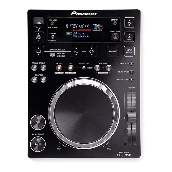
Page 10: Panel Facilities
2.3 PANEL FACILITIES CDJ-350... - Page 11 CDJ-350...
-
Page 12: Basic Items For Service
Before shipping out the product, be sure to clean the following positions by using the prescribed cleaning tools. Position to be cleaned Name Part No. Remarks Pickup lenses Cleaning liquied GEM1004 Refer to "9.4 SLOTIN MECHA SECTION". Cleaning paper GED-008 CDJ-350... -
Page 13: Pcb Locations
SMPS ASSY (SYXJ8, FLXJ, KXJ5, AXJ5) DWR1482 > 2..PNLB ASSY DWX3106 SMPS ASSY (CUXJ) DWR1481 2..JACK ASSY DWX3107 2..SLMB ASSY DWX3108 1..SLOTIN MECHA ASSY DXA2206 2..TCHB ASSY DWX3109 1..TM ASSY-S (VTM091) DXX2616 2..JOGB ASSY DWX3124 MACN ASSY DWM2391 2..MAIN ASSY DWX3105 2..CNCT ASSY DWX3111 CDJ-350... -
Page 14: Block Diagram
Gold coated ZWNN1007G28-8-06A ZWNN1007G28-9-06A Single Wire Single Wire L=60mm GRAY L=60mm WHITE DE007VE0 L=75mm CN953 CN751 VKN1265-A DKN1402-A-TFB LO+ 4 SLMB ASSY FRAME GNDS GNDS 3 GNDD LPS1 LPS1 (DWX3108) LPS2 LPS2 1.0mm Pitch L=90mm DDD1492- JACK ASSY (DWX3107) CDJ-350... - Page 15 Service Part No. PEG740A8-K ASSY (LAND) GNDD GNDD IC301 2.0mm Pitch USB_CDETFLG USB_CDETFLG L=110mm Audio DSP GNDD GNDD DSPC56371AF180 DKP3864- USBA_D_N USBA_D_N USBA_D_P USBA_D_P 1.0mm Pitch L=115mm DDD1537- V501 1.0mm Pitch L=125mm DDD1494- JA505 DKN1620-A K ASSY USB A Type X3107) CDJ-350...
-
Page 16: Overall Block Diagram
IC204 DRIVER ST1+/-, ST2+/- CN953 LO+/- LPS1, LPS2 IC103 LPS2 STEPPING MAIN CPU MOTOR (DXM1201) CN954 16bit IC101 FLASH 32MB 16bit CN751 LOADING MOTOR IN SW 16bit ASSY-S IC102 (DXX2615) SLMB ASSY SDRAM 256MB CN401 SMPS ASSY POWER SUPPLY CDJ-350... - Page 17 USB_CDETFLG IC504 High Side USB_VBUSON Switch RENC_1 TSCK RENC_2 RENCO_S TSCS IC103 MAIN CPU IC501 PANEL CPU PNRDY SLIDER MAIN_RST POWER_ON TEMPO VDET TEMPOR POWER SUPPLY 26 25 PNLB ASSY DETECT CN504 CN501 CN801 CN851 JOGB ASSY TCHB ASSY CDJ-350...
-
Page 18: Power Block Diagram
G G P P 1 1 S S 0 0 9 9 4 4 H H C C Z Z 0 0 F F IC505 5.0V IC504 SW ITCH NJM2845DL1 BD2051AFJ L L E E D D V V 5 5 0 0 1 1 32.0V D D A A T T A A F F L L PNLB ASSY CDJ-350... -
Page 19: Diagnosis
TOC If the pickup is reading the position memory will be program area, it will jump located after the unit is to the TOC area. turned ON. The first track is searched for. Playback (Muting OFF) CDJ-350... -
Page 20: Troubleshooting
If the level is "H", PANEL CPU(IC501) may be 10.10 VOLTAGES Check the level of POWER_ON signal Defective signals defective. [9] Basic operation PNLB Assy (IC501-4 pin). /SMPS Assy If the level is "L", SMPS Assy may be defective. check of CPU/DSP CDJ-350... - Page 21 FL in the PNLB Assy. 10.11 waveforms be defective. PNLB 1,2,3,4 • FLSCLK Signal errors PNLB Assy If output signal is no problem, FL (V501) may be • FLBK [9] Basic operation defective. • FLLAT check of CPU/DSP • FLSO CDJ-350...
- Page 22 [9] Basic operation Defective PANEL If the symptom persists after the above Check a mounting state of PANEL CPU(IC501). PNLB Assy check of CPU/DSP CPU (IC501) corrections, If the mounting is OK, the IC501 may be damaged. CDJ-350...
- Page 23 Cam Plate is reached, shavings Rotation Load Adjustment.” Rotation Load cam plate from the worn-out washer may have increased the friction. Replace the washer, load gear, and cam plate Adjustment. with new ones, then reassemble. CDJ-350...
- Page 24 SWs (S751/S752) may be improperly Signal errors MAIN Assy soldered or defective. If soldering is improper, — signal lines. (The LPS1 and LPS2 signals resolder them. If the symptom persists, replace the becomes "L" when the SW is set to ON.) defective parts. CDJ-350...
- Page 25 If it is correctly mounted, then it may be defective. MAIN Replace it. 5.3 Diagnosis of Traverse If the symptom persists after the above Defective pickup See “5.3 Diagnosisi of the Pickup Assy” for details. the Pickup Assy mechanism corrections, CDJ-350...
- Page 26 If the AUDIO DSP (IC301) is not operating, it may [9] Basic operation be defective. Check if the AUDIO DSP (IC301) is Defective part MAIN Assy check of CPU/DSP If the AUDIO DSP (IC301) is operating, the MAIN operating. CPU (IC103) may be defective. CDJ-350...
- Page 27 If the Reset signal is OK, but the TSCK signal is not — WAVEFORMS • Reset: RESET (IC501, Pin 12) must be ”H.” IC501 output, the PANEL CPU (IC501) may be defective. MAIN 8 • MAIN communication clock: Check the waveform of TSCK (IC501, Pin 37). CDJ-350...
-
Page 28: Diagnosis Of The Pickup Assy
5.3 DIAGNOSIS OF THE PICKUP ASSY CDJ-350... -
Page 29: Connection Check With The Pc
USB Composite Device Under “Sound, video and game controllers” USB Audio Device Human Interface Devices HID-compliant device USB Human Interface Device A communication check may be easily performed if connection is made with Device Manager displayed on the PC screen. CDJ-350... -
Page 30: About Voltage Monitoring
5 If the voltage at any power IC is abnormal, the circuit that is connected to the power IC or the power IC itself may be defective. 6 Repair the detective part. 7 Replace R569 on the PNLB Assy with R599 (return R599 to its original position). CDJ-350... -
Page 31: Service Mode
Mode for firmware updating. Two modes (one for updating using a USB memory device and one for updating using a CD-ROM) are provided. Refer to the “8.4 UPDATING OF THE FIRMWARE.” 6.2 ABOUT THE DEVICE OF CDJ-350 Device Name Function Part No. -
Page 32: Details On Service Mode
After updating is completed, set the POWER switch to OFF to quit this mode. 6) Factory reset To enter this mode, set the POWER switch to ON while holding the SOURCE SELECT USB and BACK keys pressed. For details on items to be factory-reset, see “8.3 USER SETTABLE ITEMS.” CDJ-350... - Page 33 The number of upper of FL is decreased. PLAYLIST ADD PLAYLIST BPM LOCK BPM ADJUST *1: Turn to the right. *2: Turn to the left. [3] Check mode of the load of JOG dial Refer to the "8.2 JOG DIAL ROTATION LOAD ADJUSTMENT." CDJ-350...
- Page 34 USB writing error Writing to the USB storage device failed. — — E-8709 COMMUNICATION ERROR Communication between the panel microcomputer and the main microcomputer failed. E-9101 A mechanical error (timeout) was generated during loading/unloading of a disc. LOADING TIMEOUT CDJ-350...
- Page 35 The product does not judge whether they are inferior goods at the time of service. Eject A disc is ejected. Mode Change If the MASTER TEMPO button is pushed into player operation mode, MASTER TEMPO LED will light up, and it will shift to the below-mentioned "test operation mode." CDJ-350...
- Page 36 *To start up the unit in Test mode in steps, input the commands in the following order: "Servo All Off," "Focus On," then “Spindle Kick, Tracking On." [6] Updating of the firmware Refer to the "8.4 UPDATING OF THE FIRMWARE." CDJ-350...
-
Page 37: Disassembly
(3) Remove the control panel section. Control panel section Diagnosis 27P FFC • Note on Reassembly Make styling so that 27P FFC does not insert it inward (top of MAIN Assy). 27P FFC PNLB Assy 27P FFC PNLB Assy MAIN Assy MAIN Assy CDJ-350... - Page 38 "OPEN". (3) Disconnect the two flexible cables and one connector. (4) Remove the four screws. (BPZ30P080FTB) (5) Remove the four screws. (ABZ30P060FTC) CN403 CN401 MAIN PCB stay CN201 Front (6) Remove the MAIN PCB stay. MAIN PCB stay CDJ-350...
- Page 39 Float spring G5 Float spring G5 (3) Remove the SLOTIN MECHA section. SLOTIN MECHA section Direction of the dampers when attaching them When attaching the dampers, place them so that their projections (large) face front. Projection (large) to the front Damper CDJ-350...
- Page 40 • Be sure not to lose it. • Be careful to the installation places. • Confirm it by viewing. This boss is not installation position. [2] SLOTIN MECHA Assy (1) Disconnect the flexible cable. (2) Unhook the four hooks. SLOTIN MECHA Assy CN751 CDJ-350...
- Page 41 Side A. SLOTIN MECHA Assy SLMB Assy Binder • Bottom view Bound part Side A Cable Side B Rear side Side A Side B Side A Side B CDJ-350...
- Page 42 Note on the float rubber installation Pole of the float base 05 Assy Hook ×2 Pickup lens Cleaning the pickup lens Before shipment, be sure to clean the pickup lens, using the following cleaning materials: Cleaning liquid : GEM1004 Cleaning paper: GED-008 CDJ-350...
- Page 43 Arrangement of the FFC • Pickup FFC • Spindle motor FFC Spindle motor CNCT Assy • Stepping motor FFC Stepping motor Stepping motor Pickup CNCT Assy CNCT Assy • 5P FFC SLMB Assy CNCT Assy 5P FFC CDJ-350...
- Page 44 JOG Dial Rotation Load Adjustment Mechanism About details of Adjustment etc., refer to the “8.2 JOG DIAL ROTATION LOAD ADJUSTMENT”. JOG dial rotation load adjustment mechanism Screw tightening order The other screws are random order. • Bottom view Front CDJ-350...
-
Page 45: Each Setting And Adjustment
JOG Check Mode : ON • It is the mode which judges the load (light/heavy) numerically when rotating the JOG dial. POWER ON TEMPO BACK TEMPO RANGE Mode for checking the load on the Jog dial JOG Check Mode : CANCEL POWER OFF CDJ-350... -
Page 46: User Setable Items
LIBRARY CREATOR LIBRARY/FOLDER VERSION No. — TIME MODE TIME/REMAIN AUTO CUE ON/OFF Statuses of keys CDJ/VINYL DYW1792 Flash ROM IC101 MAIN JOG MODE TEMPO RANGE ± 6 % / ±10 % / ±16 % / WIDE MASTER TEMPO ON/OFF CDJ-350... -
Page 47: Updating Of The Firmware
When the error code of "E-7024" is displayed, the recovery mode operates when performing the update procedure mentioned above again, and update is performed. In this case, please carry out by USB memory in recovery. CD-ROM cannot be used. CDJ-350... -
Page 48: Exploded Views And Parts List
Screws adjacent to b mark on product are used for disassembly. For the applying amount of lubricants or glue, follow the instructions in this manual. (In the case of no amount instructions, apply as you think it appropriate.) 9.1 PACKING SECTION SYXJ8 KXJ5 only only AXJ5 only FLXJ only CDJ-350... - Page 49 See Contrast table (2) NSP 13 Warranty Card See Contrast table (2) NSP 14 Polyethylene Bag AHG7117 (2) CONTRAST TABLE CDJ-350/SYXJ8, CUXJ, FLXJ, KXJ5 and AXJ5 are constructed the same except for the following: CDJ-350 CDJ-350 CDJ-350 CDJ-350 CDJ-350 Mark...
-
Page 50: Exterior Secion
9.2 EXTERIOR SECION Refer to “9.3 CONTROL PANEL SECTION”. SLMB CN751 Spindle Motor Pickup Assy Refer to “9.4 SLOTIN MECHA SECTION”. CDJ-350... - Page 51 21 Screw ABZ30P060FTC 22 Screw BBZ30P060FTB 23 Screw BPZ30P080FTB 24 Screw PPZ30P080FTB (2) CONTRAST TABLE CDJ-350/SYXJ8, CUXJ, FLXJ, KXJ5 and AXJ5 are constructed the same except for the following: CDJ-350 CDJ-350 CDJ-350 CDJ-350 CDJ-350 Mark Symbol and Description /SYXJ8 /CUXJ...
-
Page 52: Control Panel Section
Lubricating oil (GYA1001) MAIN CN402 Note: During reassembly, be careful not to scratch the sliding surface of the back side of the Jog dial B. (Scratches on the sliding surface may cause noise during turning of the Jog dial.) CDJ-350... - Page 53 39 USB Cover DNK5657 40 Sourse Select B Assy DXB2063 41 • • • • • 42 • • • • • 43 USB Stop Button Assy DXB2064 44 • • • • • 45 • • • • • CDJ-350...
-
Page 54: Slotin Mecha Section
(GEM1036) Dyfree Dyfree (GEM1036) (GEM1036) Lubricating oil (GYA1001) Lubricating oil (GYA1001) Cleaning liquid (GEM1004) CNCT Cleaning paper (GED-008) CN952 CNCT CN955 CNCT CN951 Note: The TM Assy-S (VTM091) is supplied only in assembly form, not as a single parts. CDJ-350... - Page 55 BPZ20P060FTC 31 Spacer POR (T3) DEB1566 32 Vessel Cushion A DEC2852 33 Vessel Cushion B DEC2853 34 Vessel Cushion C DEC2854 35 Front Sheet DED1132 36 Float Base 05 Assy DXB2068 37 Floating Rubber (SI) VEB1351 38 Binder ZCA-SKB90BK CDJ-350...
-
Page 56: Schematic Diagram
LOADING MOTOR ASSY-S (DXX2615) GNDS ZWNN1007G28-8-06A L=60mm GRAY CN953 DKN140 GNDS LPS1 LPS2 Notes C N 9 5 5 is No Mount (STBY) D K N 1 2 8 CKSSYB***K F ST2- CKSRYB***K F ST2+ CEHVQW***M F ST1+ RS1/16SS***J RS1/10SR***J ST1- CDJ-350... - Page 57 GNDS CN953 ST2+ DKN1402-A ST2- C964 (LO) 0.01u ST2- (LO) ST1+ GNDS ST1+ LPS1 ST1- LPS2 ST1- C N 9 5 5 D K N 1 2 8 8 - A (ST) ST2- (ST) ST2+ (ST) ST1+ (ST) ST1- CDJ-350...
-
Page 58: Main Assy (1/4)
A 1 0 / A P C120 ADRS1 0.1u PVCC20 C121 ADRS2 VCG1063-A ADRS3 ADRS4 C108 V S S 1 V D D 3 330p K4S561632J-UC75 GNDD ADRS5 ADRS6 ADRS7 ADRS8 V+3R3 ADRS9 ADRS10 ADRS12 ADRS13 DQMLL SDRAM(256M) Substitute GNDD H57V2562GTR-75C-K CONTROL ADRESS CDJ-350... - Page 59 R189 MAIN_RST 4:11C I N A R166 10k F O U T G N D 0 SR X101 N C 2 GNDD N C 1 GNDD GNDD DSS1193-A V+3R3B 33.00MHz GNDD R171 JTAG_RST NM SR UART V+3R3B GNDD GNDD CDJ-350...
-
Page 60: Main Assy (2/4)
R 2 8 2 R 2 8 1 R 2 8 0 GNDS GNDD R 2 7 9 R 2 7 8 R 2 7 7 INSIDE INSW V+3R3S GNDD GNDS R 2 7 6 INSIDE GNDS indic of id CDJ-350... - Page 61 RS1/10SR****F RS1/10SR***J : Voltage Measuring Point 1/4W RS1/4SA***J VCG1063A-T 1000pF/50V The > mark found on some component parts indicates the importance of the safety factor of the part. Therefore, when replacing, be sure to use parts of identical designation. CDJ-350...
-
Page 62: Main Assy (3/4)
R 3 1 7 R 3 0 5 2 2 k DATA_L (DA) GNDD (DA) (DA) DACLRCK (DA) (DA) DACDATA (DA) (DA) DACBCLK CLK11M Notes is No Mount (STBY) CKSSYB***K F CKSRYB***K F CCSRCH***J F CEHVAW***M F RS1/16SS***J RS1/16SS****D RS1/10SR***J VCG1063A-T 1000pF/50V CDJ-350... - Page 63 R 3 4 8 Q 3 0 3 N M S R R T 3 T 2 2 M GNDD GNDD V-AUDIO (V-7R6A) GNDD CPU_AUDIO 1:12B : Analog Audio Signal Route (DA) : Audio Data Signal Route : Waveform Measuring Point CDJ-350...
-
Page 64: Main Assy (4/4)
R 4 2 0 R 4 4 3 Q 4 0 5 Q 4 0 8 HN1C01FU(YGR) HN1C01FU(YGR) GNDD GNDD N O R M A L H i - Z A B N O R M A L H i 1/4W CDJ-350... - Page 65 CCSSCH***J F CEHVAW***M F RS1/16SS***J The > mark found on some component parts RS1/10SR****F indicates the importance of the safety factor of the part. RS1/10SR***J 1/4W Therefore, when replacing, be sure to use parts RS1/4SA***J of identical designation. VCG1063A-T 1000pF/50V CDJ-350...
-
Page 66: Jack Assy
CONT2 10 C714 GNDD 11 USBB_D_N 12 USBB_D_P 13 GNDD 14 VBUS_B 15 GNDD 16 C707 VA701 MUTE_1 17 470u/16 D709 RKZ5.6KG(B2) C712 GNDD GNDA (USB_DN) (USB_DP) Notes is No Mount CCSRCH***J F CEANP***M F CEAT***M F CKSRYB***K F RS1/10SR***J CDJ-350... -
Page 67: Audio Out
D708 100u/16 RKZ5.6KG(B2) GNDA GNDA CONTROL JA702 VKB1243-A (CONT1) (CONT1) R714 (CONT2) (CONT2) R715 GNDD R709 USB CONNECTOR B Type GNDD JA703 DKN1237-A (USB_DN) R707 L701 V+5DETD 1 (USB_DN) USBB_N 2 (USB_DP) (USB_DP) R708 USBB_P 3 GNDD 4 GNDD CDJ-350... -
Page 68: Pnlb Assy
DSG1079-A VSG1024-A VSG1024-A MASTER S503 S508 S512 S515 T-SEARCH + TEMPO PLAYLIST The > D527 VSG1024-A DSG1079-A VSG1024-A DSG1079-A S504 S509 indicate SEARCH - TEMPO Therefo VSG1024-A GNDD GNDD GNDF GNDD VSG1024-A of ident S505 SEARCH + VSG1024-A GNDD CDJ-350... - Page 69 USBSTOP RS1/10SR***J DSG1079-A R567 RS1/10SR****F S525 STANDBY STANDBY VSG1024-A GNDD The > mark found on some component parts indicates the importance of the safety factor of the part. Therefore, when replacing, be sure to use parts of identical designation. CDJ-350...
-
Page 70: Tchb And Jogb Assys
GNDD GP1S094HCZ0F 100k R806 GNDD GNDD GNDD NOTES is No Mount RS1/10SR***J CKSRYB***K F JOGB ASSY (DWX3124) PC851 CN851 SEDS-7573 DKP3864-A VLED JOG2 R851 C853 JOG1 0.01u GND1 GNDD Board in Connector GNDD NOTES RS1/10SR***J CKSRYB***K F CKSQYB***K F CDJ-350... - Page 71 CDJ-350...
-
Page 72: Smps Assy
The > mark found on some component parts CAUTION - FOR CONTINUED PROTECTION AGAINST RISK OF FIRE, indicates the importance of the safety factor of the part. REPLACE WITH SAME TYPE AND RATINGS OF FUSE. Therefore, when replacing, be sure to use parts of identical designation. CDJ-350... - Page 73 CDJ-350...
- Page 74 The > mark found on some component parts CAUTION - FOR CONTINUED PROTECTION AGAINST RISK OF FIRE, indicates the importance of the safety factor of the part. REPLACE WITH SAME TYPE AND RATINGS OF FUSE. Therefore, when replacing, be sure to use parts of identical designation. CDJ-350...
- Page 75 CDJ-350...
-
Page 76: Voltages
4.5 to 5.5 V D522 V+5R6 power supply circuit FL F+ 5.54 to 5.66 V (periphery of IC409) FL F- 1.98 to 2.42 V Q518, Q517 USB VBUS 4.75 to 5.25 V IC505, IC504 V+5SW 4.65 to 5.35 V D520 CDJ-350... -
Page 77: Waveforms
V: 1.0 V/div. H: 1 S/div. DISC EJECT IC103 - pin 72 (DSPDREQ) Foot of R193 (TSO) IC201 - pin 37 (RFO_TP) : upper V: 1.0 V/div. H: 20 μS/div. V: 1.0 V/div. H: 50 μS/div. PLAY V: 500 mV/div. H: 500 nS/div. CDJ-350... - Page 78 V: 1.0 V/div. H: 10 mS/div. JOG scratch V501 - pin 35 (FLBK) V501 - pin 32 (FLSO) CN501 - pin 4 (JOG2_C) V: 1.0 V/div. H: 100 μS/div. V: 1.0 V/div. H: 100 μS/div. V: 1.0 V/div. H: 10 mS/div. JOG scratch CDJ-350...
- Page 79 CDJ-350...
-
Page 80: Pcb Connection Diagram
1. The parts mounted on this PCB include all necessary parts for several destinations. For further information for respective desti- nations, be sure to check with the sche- matic diagram. 2. View point of PCB diagrams. Connector Capacitor SIDE A SIDE B P.C.Board Chip Part CDJ-350... - Page 81 SIDE B SIDE B CNCT ASSY CN955 CN954 C970 CNCT C965 DWX3111- C967 C966 C955 L951 (DNP2560-B) CN953 CN952 CN951 SLMB ASSY CN751 DWX3108- CN751 SLMB 1.LPS2 WHITE GRAY 2.LPS1 3.GNDD 4.LO+ 5.LO- SLOTSW SLOTSW ADD SOLDER (DNP2561-B) CDJ-350...
-
Page 82: Main And Jack Assys
R1004 R482 IC410 IC411 R1005 C446 R430 R1006 Q405 R499 R419 R448 R431 KN402 Q408 C452 R420 R417 IC410 IC411 IC403 IC401 IC205 Q405 Q408 JACK ASSY DWX3107- J706 JACK [[ G ]] GNDD J705 J704 C702 C701 (DNP2561-B) CDJ-350... - Page 83 V+3R3B C215 C142 C193 C134 C137 C196 A-S1 C275 C132 C133 C211 AGCRF C201 C178 R201 R276 C212 R292 R177 R240 R241 R179 C145 C261 C222 C223 C202 C260 C204 GNDS KN404 (DNP2560-B) IC205 IC103 IC105 IC404 IC104 IC201 CDJ-350...
- Page 84 R290 R238 C224 KN102 IC101 AWRC R237 R236 C220 L207 C219 R235 L208 R226 L209 C216 L210 R229 L211 R224 L212 C203 L213 L214 R281 C478 C477 (DNP2560-B) IC405 IC204 IC206 Q104 Q107 IC102 Q201 IC203 IC408 Q109 IC101 CDJ-350...
- Page 85 Q303 Q302 Q301 IC107 IC301 IC302 IC303 IC402 Q410-Q413 IC406 Q415 Q406 Q404 Q402 JACK ASSY 17.MUTE_1 16.GNDD 15.VBUS_B 14.GNDD 13.USBB_D_P 12.USBB_D_N 11.GNDD 10.CONT2 9.GNDD 8.CONT1 7.GNDD 6.MUTE_A 5.GNDA 4.LOUT GNDD 3.GNDA 2.ROUT 1.GNDA Q702 Q704 Q703 Q701 (DNP2561-B) CDJ-350...
-
Page 86: Pnlb, Tchb And Jogb Assys
GNDD V+5R6 J602 GNDD J614 J593 GNDD J536 J624 GNDD J546 J601 J522 D507 J591 V+5R6 J590 J599 J554 J523 D506 J552 J531 V+5R6 J517 GNDD V+32 J519 J545 V+5EV S505 J559 GNDD S515 S504 J598 GNDD S524 S502 CDJ-350... - Page 87 TCHB ASSY CN801 [[ G ]] PC851 DWX3109 TCHB IC801 DWX3124 JOGB (DNP2561-B) (DNP2561-B) J531 V+5R6 V+32 J519 J545 V+5EV J589 V+5R6 J512 J559 GNDD GNDD V+5EV J520 CN502 J567 GNDD CONTACT SIDE UP J598 GNDD CN502 (DNP2561-B) CN402 CDJ-350...
- Page 88 JOGB ASSY TCHB ASSY CN801 4.JOG2 1.GNDD Q801 C801 3.JOG1 D801 R804 R801 2.V+5 R802 R851 C802 R803 R805 R852 DWX3109 C851 JOGB R806 DWX3124 TCHB (DNP2561-B) (DNP2561-B) V+5R V+32 V+5R6 GNDD V+5EV GNDD CN502 Q503 Q504 E F G CDJ-350...
- Page 89 GNDD V+5EV V+5EV V+5R6 GNDD GNDD GNDD GNDD V+5R6 V+5R6 V+32 GNDD V+5EV GNDD GNDD N502 (DNP2561-B) Q516 IC506 Q515 Q513 Q519 Q512 Q514 Q517 Q502 Q501 IC502 Q507 Q508 Q518 IC501 IC504 Q505 Q506 Q510 Q509 Q511 IC505 CDJ-350...
-
Page 90: Smps Assy
11.4 SMPS ASSY SIDE A SIDE A FOR SYXJ8, FLXJ, KXJ5 and AXJ5 SMPS ASSY CDJ-350... - Page 91 SIDE B SIDE B FOR SYXJ8, FLXJ, KXJ5 and AXJ5 SMPS ASSY CDJ-350...
- Page 92 SIDE A SIDE A FOR CUXJ SMPS ASSY CDJ-350...
- Page 93 SIDE B SIDE B FOR CUXJ SMPS ASSY CDJ-350...
-
Page 94: Pcb Parts List
CTF1545 L 403 INDUCTOR CTH1254 SLMB ASSY F 101,102,301 EMI FILTER DTL1106 KN 404 WRAPPING TERMINAL CKF1089 MISCELLANEOUS X 101 CRYSTAL(33 MHz) DSS1193 S 751,752 PUSH SWITCH DSG1017 CN 751 5P CONNECTOR VKN1265 X 102 CRYSTAL (48 MHz) ASS7099 CDJ-350... - Page 95 C 144-147,151,153 CKSSYB104K10 C 418,430,467 VCG1063 C 148,169 CCSRCH100D50 C 421,434,497,1006 CCSSCH331J50 C 149,167 CCSRCH9R0D50 C 437 CKSRYB474K10 C 155-158,160 CKSSYB104K10 C 438,444,446,447 CKSSYB104K10 C 159,161,165,179 VCG1063 C 440 CKSSYB222K50 C 162-164,170,174 CKSSYB104K10 C 442,443 DCH1165 C 166,266,284,469 CKSRYB103K50 CDJ-350...
- Page 96 D 513 SPR-39MVWF(MN) D 516 SLR343BC4T(JKLM) RESISTORS D 519,520,522 1SS352 D 525 NNCD6.2MF All Resistors RS1/10SR###J MISCELLANEOUS CAPACITORS L 501-504 INDUCTOR CTF1378 C 801 CKSRYB104K16 JA 505 USB-A CONNECTOR DKN1620 V 501 DEL1072 VR 501 DCV1009 S 501-511,525 SWITCH VSG1024 CDJ-350...
- Page 97 Mark No. Description Part No. JOGB ASSY MISCELLANEOUS CN 851 CONNECTOR ASSY 4P DKP3864 RESISTORS All Resistors RS1/10SR###J MISCELLANEOUS PC 851 PHOTO INTERRUPTER SEDS-7573 CAPACITORS C 851 CKSQYB225K10 C 852,853 CKSRYB103K50 SMPS ASSY There is no service parts. CDJ-350...
Need help?
Do you have a question about the CDJ-350 and is the answer not in the manual?
Questions and answers