Sony XR-F5100 Servise Manual
Fm/am cassette car stereo
Hide thumbs
Also See for XR-F5100:
- Operating instructions manual (56 pages) ,
- Installation/connections (5 pages) ,
- Installation/connections (4 pages)
Table of Contents
Advertisement
Quick Links
QQ
3 7 63 1515 0
SERVICE MANUAL
Ver. 1.1 2006.03
AUDIO POWER SPECIFICATIONS (US model only)
POWER OUTPUT AND TOTAL HARMONIC DISTORTION
23.2 watts per channel minimum continuous average power into 4 ohms, 4 channels driven from 20 Hz to 20 kHz with no more than 5% total
harmonic distortion.
TE
L 13942296513
Cassette Player section
Tape track
Wow and flutter
Frequency response
Signal-to-noise ratio
Tuner section
FM
Tuning range
US model:
Except US model:
Antenna terminal
Intermediate frequency
Usable sensitivity
Selectivity
Signal-to-noise ratio
Harmonic distortion at 1 kHz
Separation
Frequency response
AM (US model)
Tuning range
Antenna terminal
Intermediate frequency
Sensitivity
www
.
Sony Corporation
9-877-608-02
2006C05-1
eVehicle Division
© 2006.03
Published by Sony Techno Create Corporation
http://www.xiaoyu163.com
MW (Except US model)
Tuning range
4-track 2-channel stereo
0.08 % (WRMS)
30 − 18,000 Hz
Cassette type
Sensitivity
TYPE II, IV
61 dB
TYPE I
58 dB
SW (Except US model)
Tuning range
87.5 − 107.9 MHz
Aerial terminal
FM tuning interval:
Intermediate frequency
50 kHz/200 kHz switchable
87.5 − 108.0 MHz
Sensitivity
(at 50 kHz step)
Power amplifier section
87.5 − 107.9 MHz
(at 200 kHz step)
Outputs
External antenna connector
10.7 MHz/450 kHz
Speaker impedance
9 dBf
Maximum power output
75 dB at 400 kHz
General
67 dB (stereo),
69 dB (mono)
Outputs
0.5 % (stereo),
0.3 % (mono)
35 dB at 1 kHz
30 − 15,000 Hz
530 − 1,710 kHz
External antenna connector
10.7 MHz/450 kHz
30 µV
x
ao
y
i
http://www.xiaoyu163.com
XR-F5100
8
Model Name Using Similar Mechanism
Tape Transport Mechanism Type
SPECIFICATIONS
Q Q
3
6 7
1 3
MW tuning interval:
9 kHz/10 kHz switchable
531 − 1,602 kHz
(at 9 kHz step)
530 − 1,710 kHz
(at 10 kHz step)
30 µV
SW tuning interval:
SW1: 2,940 − 7,735 kHz
SW2: 9,500 − 18,135 kHz
(except for
10,140 − 11,575 kHz)
External aerial connector
10.7 MHz/450 kHz
30 µV
Speaker outputs
(sure seal connectors)
4 − 8 ohms
52 W × 4 (at 4 ohms)
Audio output terminals
(rear/sub switchable)
Power antenna relay control
terminal
Power amplifier control
terminal
FM/AM CASSETTE CAR STEREO
FM/MW/SW CASSETTE CAR STEREO
u163
.
2 9
9 4
2 8
Chinese Model
1 5
0 5
8
2 9
9 4
Inputs
Telephone ATT control
terminal
Remote controller input
terminal
BUS control input terminal
BUS audio input terminal
Antenna input terminal
Tone controls
Low:
±10 dB at 60 Hz (XPLOD)
Mid:
±10 dB at 1 kHz (XPLOD)
High:
±10 dB at 10 kHz (XPLOD)
Power requirements
12 V DC car battery
(negative ground)
Approx. 178 × 50 × 177 mm
Dimensions
(7
(w/h/d)
Approx. 182 × 53 × 161 mm
Mounting dimensions
(7
(w/h/d)
Mass
Approx. 1.2 kg
(2 lb 10 oz)
Supplied accessories
Card remote commander
RM-X115
Parts for installation and
connections (1 set)
Front panel case (1)
Note
This unit cannot be connected to a digital preamplifier
or an equalizer which is Sony BUS system compatible.
Design and specifications are subject to change
without notice.
E, Chinese models
m
co
9 9
CA
US Model
E Model
NEW
MG-25L-136
2 8
9 9
× 2 × 7 in)
1
/
8
× 2
× 6
1
1
3
/
/
/
in)
4
8
8
US model
Advertisement
Table of Contents

Related Manuals for Sony XR-F5100


Summary of Contents for Sony XR-F5100
- Page 1 0.5 % (stereo), Power antenna relay control This unit cannot be connected to a digital preamplifier 0.3 % (mono) terminal or an equalizer which is Sony BUS system compatible. Separation 35 dB at 1 kHz Power amplifier control 30 − 15,000 Hz...
-
Page 2: Table Of Contents
XR-F5100 3 7 63 1515 0 TABLE OF CONTENTS SERVICING NOTES SERVICING NOTES SERVICE POSITION ............2 In checking the control board and main board, prepare two jigs (extension (MD) cord J-2502-060-1 and GENERAL connection cable for F/P to main J-2502-072-1). -
Page 3: General
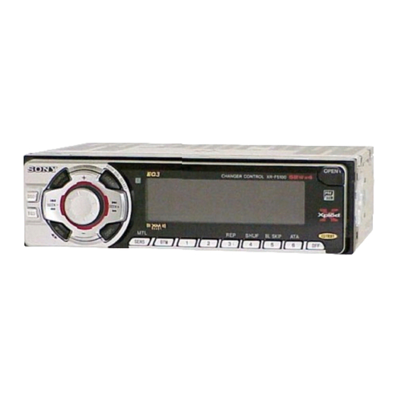
XR-F5100 SECTION 1 This section is extracted from instruction manual. 3 7 63 1515 0 GENERAL Card remote commander RM-X115 Location of controls DSPL MODE SEEK SEEK OPEN PRESET SENS SOURCE SEEK SEEK SEEK SEEK PRESET SHUF BL SKIP... - Page 4 XR-F5100 3 7 63 1515 0 Source selector* Sélecteur de source* XA-C30 L 13942296513 * not supplied non fourni Cautions Connection example (2) • This unit is designed for negative ground 12 V Notes (2-A) DC operation only. • Be sure to connect the ground lead before •...
-
Page 5: Q Q
XR-F5100 3 7 63 1515 0 Source selector (not supplied) Supplied with the CD/MD changer Sélecteur de source Fourni avec le changeur de CD/MD (non fourni) Supplied with XA-C30 XA-C30 Fourni avec le XA-C30 from car antenna à partir de l’antenne de la voiture... - Page 6 XR-F5100 3 7 63 1515 0 Orient the release key correctly. Orientez correctement la clé de déblocage. Face the hook inwards. Tournez le crochet vers l’intérieur. Dashboard Tableau de bord 1 8 2 5 3 m Claws Griffes L 13942296513 max.
- Page 7 Japanese cars. In such a case, consult Cet appareil ne peut pas être installé dans your Sony dealer. certaines voitures japonaises. Consultez, dans L 13942296513 ce cas, votre détaillant Sony. Note To prevent malfunction, install only with the Remarque supplied screws 2.
-
Page 8: 2-4. Main Board
XR-F5100 SECTION 2 DISASSEMBLY 3 7 63 1515 0 • This set can be disassembled in the order shown below. 2-1. DISASSEMBLY FLOW FRONT PANEL SECTION Note: Illustration of disassembly is omitted. 2-2. SUB PANEL SECTION (Page 8) 2-3. MECHANISM DECK (MG-25L-136) (Page 9) 2-4. -
Page 9: Mechanism Deck (Mg-25L-136)
XR-F5100 3 7 63 1515 0 2-3. MECHANISM DECK (MG-25L-136) 4 mechanism deck 3 screw (PTT2.6 × 6) (MG-25L-136) 1 flexible board (CN351) 2 flexible board (CN301) L 13942296513 2-4. MAIN BOARD 2 two screws (PTT2.6 × 6) 1 rubber cap (25) 4 three screws (BTT2.6 ×... -
Page 10: Assembly
XR-F5100 SECTION 3 ASSEMBLY 3 7 63 1515 0 • This set can be assembled in the order shown below. 3-1. ASSEMBLY FLOW 3-2. HOUSING (Page 11) 3-3. ARM (SUCTION) (Page 11) 3-4. LEVER (LDG-A)/(LDG-B) (Page 12) 3-5. GEAR (LDG-FT) (Page 12) 3-6. -
Page 11: Housing
XR-F5100 3 7 63 1515 0 Note: Follow the assembly procedure in the numerical order given. 3-2. HOUSING 7 Hold the hanger by bending the claw. 5 Fit projection on C part. 1 Install the catch to the hanger. -
Page 12: Lever (Ldg-A)/(Ldg-B)
XR-F5100 3 7 63 1515 0 3-4. LEVER (LDG-A) / (LDG-B) shaft A shaft A shaft B shaft B shaft C 1 Fit the lever (LDG-A) on 3 type-E stop ring 2.0 shafts A – C and install it. -
Page 13: Guide (C)
XR-F5100 3 7 63 1515 0 3-6. GUIDE (C) 2 guide (C) 1 three claws L 13942296513 3-7. MOUNTING POSITION OF CAPSTAN/REEL MOTOR (M901) two precision screws (P2 × 2) capstan/reel motor (M901) Note: Mount the motor so that the... -
Page 14: Mechanical Adjustments
XR-F5100 SECTION 4 SECTION 5 MECHANICAL ADJUSTMENTS 3 7 63 1515 0 ELECTRICAL ADJUSTMENTS 1. Clean the following parts with a denatured-alcohol-moistened TAPE DECK SECTION 0 dB= 0.775 V swab: playback head pinch roller 1. The adjustments should be performed in the order given in... -
Page 15: Tuner Section
XR-F5100 3 7 63 1515 0 TAPE SPEED ADJUSTMENT Setting: test tape WS-48A frequency counter (3 kHz, 0 dB) 4 Ω – speaker out terminal Procedure: 1. Put the set into the FWD PB mode. 2. Adjust adjustment resistor for inside capstan motor so that the reading on the frequency counter becomes in 3,015 Hz. -
Page 16: Display Board
XR-F5100 Ver. 1.1 SECTION 6 DIAGRAMS 3 7 63 1515 0 6-1. NOTE FOR PRINTED WIRING BOARDS AND SCHEMATIC DIAGRAMS Note on Printed Wiring Board: Note on Schematic Diagram: • All capacitors are in µF unless otherwise noted. (p: pF) •... -
Page 17: Mechanism Deck
:Uses unleaded solder. • Semiconductor Location Ref. No. Location D352 I-14 CN581 J331 D401 BUS CONTROL IN BUS AUDIO IN AUDIO OUT REAR (FOR SONY BUS) D479 F-10 J671 F901 D581 H-14 REMOTE D582 H-14 (FRONT VIEW) FM/AM D584 G-13... -
Page 18: Schematic Diagram - Main Board (1/3)
XR-F5100 Ver. 1.1 3 7 6 3 1 5 1 5 0 6-3. SCHEMATIC DIAGRAM – MAIN Board (1/3) – • See page 24 for IC Block Diagrams. J331 (1/3) AUDIO AUDIO TUX-032//Q (US) REAR TUX-032//Q2 (E, EA, CH) -
Page 19: Schematic Diagram - Main Board (2/3)
XR-F5100 Ver. 1.1 3 7 6 3 1 5 1 5 0 6-4. SCHEMATIC DIAGRAM – MAIN Board (2/3) – • • • See page 16 for Waveforms. See page 24 for IC Block Diagrams. See page 25 for IC Pin Function Description. -
Page 20: Schematic Diagram - Main Board (2/3)
SIRCS KEY0 R710 (Page 19) R586 (Page 21) KEY-0 KEY1 R711 KEY-1 RE_IN0 R724 C581 R584 RE-0 0.47 FLASH-W R702 SONY BUS INTERFACE R701 C582 0.047 D701 MMDL914T1 JW95 JW93 (CHASSIS) D581 R581 MM3Z6V2ST1 D582 R582 MM3Z18VST1 Q581 MUN2211T1 BATTERY... -
Page 21: Printed Wiring Board - Sub Board
XR-F5100 3 7 6 3 1 5 1 5 0 6-7. SCHEMATIC DIAGRAM – SUB Board – 6-6. PRINTED WIRING BOARD – SUB Board – :Uses unleaded solder. SUB BOARD (COMPONENT SIDE) LSW801 SUB+B CNP801 DOOR-SW D_SW KEY+B CNP801... -
Page 22: Printed Wiring Board - Display Board
XR-F5100 3 7 6 3 1 5 1 5 0 6-8. PRINTED WIRING BOARD – DISPLAY Board – :Uses unleaded solder. DISPLAY BOARD (COMPONENT SIDE) S919 S902 SOURCE DISC/PRESET IC951 LCD901 LED908 S903 LED910 LIQUID CRYSTAL DISPLAY LIST LED909... -
Page 23: Schematic Diagram - Display Board
XR-F5100 Ver. 1.1 3 7 6 3 1 5 1 5 0 6-9. SCHEMATIC DIAGRAM – DISPLAY Board – • See page 16 for Waveform. IC905 MM3033D VOUT R951 R925 R926 R928 R927 R971 R973 R975 R977 R979 R981 R952 2.2k... - Page 24 XR-F5100 3 7 6 3 1 5 1 5 0 • IC Block Diagrams – MAIN Board – IC751 TDA8588J/N1 IC351 LB1930M-TLM-E IC581 MM1175XFF IC301 HA12231FPEL BUS ON BUFFER RESET RESET RESET OUT1 OUT-FL- MOTOR C BUS SWITCH CONTROL...
- Page 25 Serial data output to the SONY bus interface BUSSI Serial data input from the SONY bus interface BUSCKO Serial data transfer clock signal output to the SONY bus interface u163 I2C_SIO IIC two-way data bus with the tuner pack, electrical volume and power amplifier...
- Page 26 XR-F5100 3 7 63 1515 0 Pin No. Pin Name Description Not used Muting on/off control signal output terminal Not used Automatic music sensor detection signal output terminal AMSON “L”: music is present, “H”: music is not present N_ROUT Tape direction control signal output terminal “L”: reverse, “H”: forward...
-
Page 27: Exploded Views
XR-F5100 Ver. 1.1 SECTION 7 EXPLODED VIEWS 3 7 63 1515 0 NOTE: • Items marked “*” are not stocked since they • -XX and -X mean standardized parts, so they may have some difference from the original are seldom required for routine service. Some one. -
Page 28: 7-2. Front Panel Section
XR-F5100 Ver. 1.1 3 7 63 1515 0 7-2. FRONT PANEL SECTION not supplied (DISPLAY board) RE901 not supplied LCD901 supplied CN901 supplied L 13942296513 not supplied supplied Ref. No. Part No. Description Remark Ref. No. Part No. Description... -
Page 29: Mechanism Deck Section (Mg-25L-136)
XR-F5100 3 7 63 1515 0 7-3. MECHANISM DECK SECTION (MG-25L-136) HP901 M901 L 13942296513 not supplied Ref. No. Part No. Description Remark Ref. No. Part No. Description Remark A-3315-400-C FLYWHEEL (HR) ASSY 3-933-344-24 GUIDE (C) * 152 3-019-130-01 LEVER (LDG-A) -
Page 30: Electrical Parts List
XR-F5100 Ver. 1.1 SECTION 7 3 7 63 1515 0 ELECTRICAL PARTS LIST DISPLAY NOTE: When indicating parts by reference • Due to standardization, replacements in the • Items marked “*” are not stocked since they number, please include the board. - Page 31 XR-F5100 Ver. 1.1 3 7 63 1515 0 DISPLAY MAIN Ref. No. Part No. Description Remark Ref. No. Part No. Description Remark R927 1-216-817-11 METAL CHIP 1/10W A-3283-586-A MAIN BOARD, COMPLETE (E, CH) R928 1-216-817-11 METAL CHIP 1/10W A-3283-616-A MAIN BOARD, COMPLETE (EA)
- Page 32 XR-F5100 Ver. 1.1 MAIN 3 7 63 1515 0 Ref. No. Part No. Description Remark Ref. No. Part No. Description Remark C412 1-136-154-00 FILM 0.012uF C759 1-124-584-00 ELECT 100uF C413 1-162-965-11 CERAMIC CHIP 0.0015uF 10% C762 1-125-891-11 CERAMIC CHIP 0.47uF...
- Page 33 XR-F5100 3 7 63 1515 0 MAIN Ref. No. Part No. Description Remark Ref. No. Part No. Description Remark IC401 6-705-372-01 IC BD3808FS-FE2 < RESISTOR > IC501 6-804-099-01 IC MN101C49KSS IC581 8-759-096-16 IC MM1175XFF 1-247-807-31 CARBON 1/4W 1-247-807-31 CARBON...
- Page 34 XR-F5100 Ver. 1.1 3 7 63 1515 0 MAIN Ref. No. Part No. Description Remark Ref. No. Part No. Description Remark R516 1-216-845-11 METAL CHIP 100K 1/10W R654 1-216-833-11 METAL CHIP 1/10W R518 1-216-845-11 METAL CHIP 100K 1/10W R671...
- Page 35 XR-F5100 Ver. 1.1 3 7 63 1515 0 Ref. No. Part No. Description Remark Ref. No. Part No. Description Remark MISCELLANEOUS ************** 1-792-195-31 CABLE, FLEXIBLE FLAT (14 CORE) 1-776-207-82 CORD (WITH CONNECTOR) (POWER) 1-780-097-11 CONDUCTIVE BOARD, CONNECTION A-3220-811-A MECHANISM DECK ASSY (MG-25L-136)
- Page 36 XR-F5100 3 7 63 1515 0 REVISION HISTORY Clicking the version allows you to jump to the revised page. Also, clicking the version at the upper right on the revised page allows you to jump to the next revised page.
Need help?
Do you have a question about the XR-F5100 and is the answer not in the manual?
Questions and answers