Philips HTS8100 Service Manual
Hide thumbs
Also See for HTS8100:
- User manual (56 pages) ,
- Manual (3 pages) ,
- Quick start manual (2 pages)
Table of Contents
Advertisement
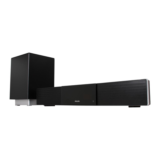
DVD Home Theater System
CLASS 1
LASER PRODUCT
Contents
1
2
3
4
5
6
7
© Copyright 2007 Philips Consumer Electronics B.V. Eindhoven, The Netherlands.
All rights reserved. No part of this publication may be reproduced, stored in
a retrieval system or transmitted, in any form or by any means, electronic,
mechanical, photocopying, or otherwise without the prior permission of Philips.
Published by KK 710 V&MA
Version 1.0
Page
Contents
2
2
4
5
9
10
14
15
19
33
8
35
35
36
37
38
39
39
41
43
44
Printed in the Netherlands
HTS8100
Subject to modification
/
05/12/37/59
Page
45
48
50
53
55
59
61
62
63
65
67
68
71
71
72
73
EN 3139 785 32540
Advertisement
Table of Contents

Related Manuals for Philips HTS8100


Summary of Contents for Philips HTS8100
-
Page 1: Table Of Contents
PWB Layout: USB PWB Layout: Door Control Board © Copyright 2007 Philips Consumer Electronics B.V. Eindhoven, The Netherlands. All rights reserved. No part of this publication may be reproduced, stored in a retrieval system or transmitted, in any form or by any means, electronic, mechanical, photocopying, or otherwise without the prior permission of Philips. -
Page 2: Technical Specifications And Connection Facilities
EN 2 3139 785 32540 Technical Specifi cations and Connection Facilities LOCATION OF PC BOARDS Front Board DVD Mechanism Door Control Board PCBs on the lower level Front Keys Board AV Board SD9.2 MPEG Board HDMI Board Front LED Board USB Board SCART Board (/12/05) AVIO Board (/37/59) - Page 3 3139 785 32540 EN 3 TUNER MODULE POWER BOX SPEAKER BOARD AIO BOARD AMPLIFIER MODULE AV BOARD VERSION VARIATIONS: HTS8100/37 HTS8100/59 HTS8100/05/12 Video (Yellow, Cinch) SCART (CVBS/RGB) TV AUDIO IN (TV 2) AUDIO IN (LEFT/RIGHT) 110-127V~220~240V VOLTAGE SELECTOR switch (Power Box)
-
Page 4: Technical Specifications
EN 4 3139 785 32540 Technical Specifi cations and Connection Facilities 1. Specifi cations General: COMPACT DISC/VCD/DVD: Power Supply Rating : 220-240V; 50-60 Hz Video Decoding : MPEG-1/MPEG-2/ (/05/12) DivX 3/4/5/6, Ultra : 120V; 60 Hz (/37) Video DAC : 12 Bits : 110-127V/220-240V Signal System : PAL / NTSC... -
Page 5: Measurements Setup, Service Aid & Lead Free Requirements
Measurements Setup, Service Aid & Lead Free Requirements 3139 785 32540 EN 5 2. Measurements Setup, Service Aid & Lead Free Requirements MEASUREMENT SETUP Tuner FM Bandpass LF Voltmeter 250Hz-15kHz e.g. PM2534 e.g. 7122 707 48001 RF Generator e.g. PM5326 S/N and distortion meter e.g. - Page 6 EN 6 3139 785 32540 Measurements Setup, Service Aid & Lead Free Requirements SERVICE AIDS Service Tools: Universal Torx driver holder ........4822 395 91019 Torx bit T10 150mm ..........4822 395 50456 Torx driver set T6 - T20 ......... 4822 395 50145 Torx driver T10 extended ........
- Page 7 Measurements Setup, Service Aid & Lead Free Requirements 3139 785 32540 EN 7 WAARSCHUWING WARNING Alle IC’s en vele andere halfgeleiders zijn All ICs and many other semi-conductors are gevoelig voor electrostatische ontladingen (ESD). susceptible to electrostatic discharges (ESD). Onzorgvuldig behandelen tijdens reparatie kan Careless handling during repair can reduce life de levensduur drastisch doen verminderen.
- Page 8 Due to lead-free technology some rules have to be respected by the workshop during a repair: • Use only lead-free solder alloy Philips SAC305 with order code 0622 149 00106. If lead-free solder-paste is required, please contact the manufacturer of your solder-equipment.
-
Page 9: Service Hints For Replacing Defective Loader
Measurements Setup, Service Aid & Lead Free Requirements 3139 785 32540 EN 9 2.2 Service Hints 2.2.1 Service Hints for Replacing Defective Loader CAUTION CHARGED CAPACITORS ON THE SERVO BOARD MAY DAMAGE THE DRIVE ELECTRONICS WHEN CONNECTING A NEW DRIVE.THAT’S WHY, BESIDES THE SAFETY MEASURES LIKE •... -
Page 10: Service Hints For Power Box Cable Dressing
EN 10 3139 785 32540 Measurements Setup, Service Aid & Lead Free Requirements 2.2.2 Service Hints for Power Box Cable Dressing The following procedures should be followed for Power Box Module assembly after being repaired. 3) Fold as indicated underneath the metal chassis for both 1) For the 5 and 12 poles cables to Audio BD, paste a tape point 1) and 2). - Page 11 Measurements Setup, Service Aid & Lead Free Requirements 3139 785 32540 EN 11 5) For the FFC cables from the Audio BD to Tuner/Speaker/ 7) For reference to point 6). AIO BD, fold as indicated, hence, preventing them from touching the Audio BD itself. Figure 2-7 Figure 2-5 8) The cables should be tied as indicated.
- Page 12 EN 12 3139 785 32540 Measurements Setup, Service Aid & Lead Free Requirements 9) With reference to point 8), all cables should refrain from 11) Paste a tape over the subwoofer cable on the Tuner as touching or even getting near to the PSU. indicated.
- Page 13 Measurements Setup, Service Aid & Lead Free Requirements 3139 785 32540 EN 13 13) With reference to point 11). Note that the cable should not be bent to the left across the Audio BD due to the excess cable when the unit is being push back inside the wooden Power Box.
-
Page 14: Service Hints For Dismantling Of Main Unit
EN 14 3139 785 32540 Measurements Setup, Service Aid & Lead Free Requirements 2.2.3 Service Hints for Dismantling of Main Unit Before dismantling the main unit, unscrew the screws and detach the door panel assembly (120+121) as shown in the fi... -
Page 15: Directions For Use
3.1. Directions For Use /05/12 The following except of the Quick Use Guide serves as an introduction to the set. The Complete Direction for the Use can be downloaded in different languages from the internet site of Philips Customer care Center: www.p4c.philips.com... - Page 16 EN 16 3139 785 32540 Directions for Use...
- Page 17 3.2. Directions For Use /37/59 The following except of the Quick Use Guide serves as an introduction to the set. The Complete Direction for the Use can be downloaded in different languages from the internet site of Philips Customer care Center: www.p4c.philips.com...
- Page 18 EN 18 3139 785 32540 Directions for Use...
-
Page 19: Dismantling Instructions & Service Positions
Dismantling Instructions & Service Positions 3139 785 32540 EN 19 Mechanical Instructions Notes: The position numbers used in the instructions refer to the exploded view drawings in Chapter 8. Follow the Service Hints in Chapter 2 for dismantling the Main Unit, replacing the defective DVD mechanism and the Power Box Cable Dressing. - Page 20 EN 20 3139 785 32540 Dismantling Instructions & Service Positions 4.1.2 Dismantling of SD9.2 MPEG board and AV board 1) In order to dismantle the SD9.2 Mono Board1070, it is 3) Remove 5 screws to detach the AVIO (SCART) necessary to remove the Rear Cabinet and the HDMI and AV assembly (1040+135+1020 for /05/12, and assembly (1060 +134).
- Page 21 Dismantling Instructions & Service Positions 3139 785 32540 EN 21 4.1.3 Dismantling of Door Board, Motor Assembly, DVD Mechanism, and Front Board 3) Remove 4 screws to dismount the DVD assembly (127+ 1) Remove the Rear Cover fi rst (fi gure 1), remove the HDMI 129 +1080) as shown in fi...
- Page 22 EN 22 3139 785 32540 Dismantling Instructions & Service Positions Summary of Dismantling Instructions (4.1.1 to 4.1.3) Door Cover 200-49/Rear Cover 200-47 (Speaker Box Assembly Exploded View) Remove 10 screws Ref: 4.1.1 PC Boards on the Rear Frame HDMI/AVIO/AV/SD 9.2 HDMI 1060 Remove 4 screws AVIO 1030/ SCART 1040...
- Page 23 Dismantling Instructions & Service Positions 3139 785 32540 EN 23 4.1.4. Dismantling of USB Board and IPOD Board 3) Remove 3 screws to detach the Bracket 140 together with 1) In order to dismantle the USB Board 1013 and IPOD USB Board 1013 as shown in fi...
- Page 24 EN 24 3139 785 32540 Dismantling Instructions & Service Positions Dismantling of the Speaker Box Assembly Remove 9 more screws from the Rear Cabinet (5 screws 1) It is necessary to remove the Rear Cover and all the on the right and 4 screws on the left as shown in fi gure main unit components (PC Boards together with the 19-a and 19-b) to detach 2 Speaker Grilles together with Brackets) to dismantle the Speaker Box Assembly without...
- Page 25 Dismantling Instructions & Service Positions 3139 785 32540 EN 25 5) Remove 4 screws at the front (Make sure that all 4 Grommets are removed together with the Grilles; 2 screws on the right and 2 screws on the left as shown in fi...
- Page 26 EN 26 3139 785 32540 Dismantling Instructions & Service Positions 4.2.1. Dismantling of the right Speaker Module and the interface board In order to dismantle the Right Speaker Module (Right 3) After taking out the speakers and removing the screws, Speaker Rear Cabinet + Right Speaker Front Panel + Right the Right Metal Partition should be detached by removing Speaker Units), it is necessary to unscrew the screws hidden...
- Page 27 Dismantling Instructions & Service Positions 3139 785 32540 EN 27 4.2.2. Dismantling of the left Speaker Module 1) In order to dismantle the Left Speaker Module (Left Speaker Rear Cabinet + Left Speaker Front Panel + Left Speaker Units), remove 8 screws fi rst, take out the Surround and Center Speakers and remove 4 more screws inside the Speaker Cabinet.
- Page 28 EN 28 3139 785 32540 Dismantling Instructions & Service Positions Summary of Dismantling Instructions (4.2, 4.2.1, 4.2.2) Rear Cover PC Boards on the Rear Frame Rear Frame PC Boards on the lower level, DVD Door Panel and Door Panel Holder 120+121 Mechanism Ref: 2.2.3...
- Page 29 Dismantling Instructions & Service Positions 3139 785 32540 EN 29 Dismantling of the Subwoofer Power Box 1) Loosen 5 screws at the base of the Subwoofer (as shown in fi gure 14) and remove 5 screws at the back (as shown in fi...
- Page 30 EN 30 3139 785 32540 Dismantling Instructions & Service Positions 4) To dismantle the PSU 1030, it is necessary to dismantle the Bottom Plate Assembly (1030 +161) from the Rear Plate 230 (remove 3 screws as shown in fi gure 19) and the bracket 236 (remove 3 screws from both sides of the bracket 236 as shown in fi...
-
Page 31: Service Positions
Dismantling Instructions & Service Positions 3139 785 32540 EN 31 Service Positions Notes: The AVIO (SCART) bracket 135, the HDMI bracket 134 and the rear frame 132 should be removed for main unit service positions. Refer to the set-wiring diagram for the correct cable connection between boards. - Page 32 EN 32 3139 785 32540 Dismantling Instructions & Service Positions IO Board AV Board Speaker Board Figure 4-31 Power Box Service Position 5 Audio Board, IO Board and Speaker Board Figure 4-32 Power Box Service Position 6...
-
Page 33: Service Test Program
Service Test Program 3139 785 32540 EN 33 Service Test Program To start Service Test Program, refers to Service Mode power up the set, open the tray refers to Version with remote control or front xx refers to Software version number of BEA panel key and press 2,5,8 on the (counting up from 01 to 99) remote control. - Page 34 <9> <9> <9> <9> <AUDIO> <2> ...for HTS8100/37 2. Press the <DISPLAY> button on the Remote Control. <9> <9> <9> <9> <AUDIO> <3> ...for HTS8100/59 LATAM 3. The fi rmware version will be displayed on the top left hand corner <9>...
-
Page 35: Block Diagram And Wiring Diagram
Block Diagram, Wiring Diagram 3139 785 32540 EN 35 Main Unit Block Diagram 3139-249-39381-130-A3-sh1.pdf 2007-03-05... -
Page 36: Power Box Block Diagram
FAN SWITCH TU_RDS_CLK FAN_CTRL CIRCUIT TU_RDS_DATA FR/FL, SR/SL Analog Analog Signal AUDIO BOARD Signal TO subwoofer SPEAK BOARD TO HTS8100 one Bar Speaker FR/FL/SL/SR/CEN TO HTS8100 one Bar Speaker Sono-wave speaker connector( HTS6600 FR/SR/CEN FL/SL/CEN 3139-249-40141-130-A3 pbx.pdf 2006-08-04 Sono-wave speaker... -
Page 37: Main Unit Wiring Diagram
Block Diagram, Wiring Diagram 3139 785 32540 EN 37 Main Unit Wiring Diagram 1104 Front LED +5VL FRONT DISPLAY 1102 Class 2, 1-Layer FRONT_SDA Class 3, 2-layer FRONT_SCL 140mm X 50mm FRONT KEYS LED_STDBY_R LED_STDBY_RD FRONT_IRQ +12V 1100 LED_ON_BL LED_ON_BL Class 2 -24V +5VSTBY... -
Page 38: Power Box Wiring Diagram
1207 (hts8100/6600) 3139 110 36051 FRONT UART_TX FFC FOIL 04P/080/04P AD AMP_RST UART_CTS 8007 UART_RTS Remarks : HTS8100/6600- 1207 is inserted; FREQ_HOP HTS5950-1206 is inserted. 1208 and 1206 is at same location, optional insertion. 1302 1206( hts5950) 8P FFC 1.25 1100 5P FFC 1.25... -
Page 39: Circuit Diagram And Pwb Layout
Circuit Diagram and PWB Layout 3139 785 32540 EN 39 Main Unit Front Board: Circuit Diagram (Part 1) 1100 C2 7106 F12 1102 A2 7107 F12 1104 F1 7108 F13 1105 F6 7109 H13 1106 C5 7110 H3 1107 H2 7111 C4 1108 A11 F101 C2... - Page 40 Circuit Diagram and PWB Layout 3139 785 32540 EN 40 Front Board: Circuit Diagram 1302 A1 1200 C2 1303 A3 1201 B2 1304 D1 1203 C3 1305 D3 1204 D2 2301 B2 2200 B3 2302 B2 2201 C2 2303 D2 F201 C3 2304 D2 F202 C2...
-
Page 41: Front Board
Circuit Diagram and PWB Layout 3139 785 32540 EN 41 Front Board PWB Layout: Front Display (Top view) Front Display 3139-243-35943-top-a3.pdf_2007-03-05... - Page 42 Circuit Diagram and PWB Layout 3139 785 32540 EN 42 Front Board PWB Layout: Front Display (Bottom view) Front Display 3139-243-35943-bot-a3.pdf_2007-03-05...
-
Page 43: Pwb Layout: Usb
Circuit Diagram and PWB Layout 3139 785 32540 EN 43 Front Board Front Board PWB Layout: USB (Top view) PWB Layout: USB (Bottom view) USB 3139-243-35923-top-a4.pdf_2007-03-05 USB 3139-243-35923-bot-a4.pdf_2007-03-05... -
Page 44: Pwb Layout: Door Control Board
Circuit Diagram and PWB Layout 3139 785 32540 EN 44 Front Board Front Board PWB Layout: Door Control Board (Top view) PWB Layout: Door Control Board (Bottom view) Door Control Board 3139-243-35903-bot-a4.pdf_2007-03-05 Door Control Board 3139-243-35903-top-a4.pdf_2007-03-05... -
Page 45: Av Board: Circuit Diagram (Part 1 To Part 3)
Circuit Diagram and PWB Layout 3139 785 32540 EN 45 AV Board: Circuit Diagram (Part 1) 1100 C1 F131 D12 1102 A8 F132 D12 1104 C13 F133 B8 1105 A12 2100 D3 2101 D3 2102 C4 2103 C2 2104 C2 2105 B2 +5VL 2106 B2... - Page 46 Circuit Diagram and PWB Layout 3139 785 32540 EN 46 AV Board: Circuit Diagram (Part 2) 1200 A2 1201 C12 1202 C11 1203 F12 1204 A1 1205 C1 2200 E3 2201 E3 2202 E4 2203 E4 2204 E6 5203 1204 1200 2205 E6 F200...
- Page 47 Circuit Diagram and PWB Layout 3139 785 32540 EN 47 AV Board: Circuit Diagram (Part 3) 1300 E1 3377 E1 1301 A2 4301 C3 1303 B2 4302 D1 2300 A2 4303 A1 -12V 2301 A3 4304 A6 2302 A3 4305 A6 4304 +12V 2303 C4...
-
Page 48: Pwb Layout: Av Board
Circuit Diagram and PWB Layout 3139 785 32540 EN 48 PWB Layout: AV Board (Top view) AV 3139-243-35847-top-a3.pdf_2007-02-13... - Page 49 Circuit Diagram and PWB Layout 3139 785 32540 EN 49 PWB Layout: AV Board (Bottom view) AV 3139-243-35847-bot-a3.pdf_2007-02-13...
-
Page 50: Sd 9.2 Board: Circuit Diagram (Part 1 To Part 3)
Circuit Diagram and PWB Layout 3139 785 32540 EN 50 SD 9.2 Board: Circuit Diagram (Part 1) 1101 D1 3109 A12 3527-3 H11 T142 E6 1102 F1 3110 A10 3527-4 H11 T143 C6 1103 H1 3111 A12 3528-1 G12 T155 I10 HDMI_SW 1104 I10 3112 A8... - Page 51 Circuit Diagram and PWB Layout 3139 785 32540 EN 51 SD 9.2 Board: Circuit Diagram (Part 2) 1201 D5 3262 G11 1203 A12 3265 B10 1205 B7 3266 C10 1206 B8 3267 E1 1208 B8 3268 H11 1209 A11 3269 H11 1210 A12 3271 A10 R_Cr_Pr...
- Page 52 Circuit Diagram and PWB Layout 3139 785 32540 EN 52 SD 9.2 Board: Circuit Diagram (Part 3) 1301 D6 T335 F11 1302 D12 T336 G11 2320 B7 T337 G11 2324 A5 T338 G11 2332 B5 T339 G11 4303 2334 D4 T340 G11 2335 D4 T341 G11...
-
Page 53: Pwb Layout: Sd 9.2 Board
Circuit Diagram and PWB Layout 3139 785 32540 EN 53 PWB Layout: SD 9.2 Board (Top view) SD9.2 3139-243-35826-top-a3.pdf_2007-02-13... - Page 54 Circuit Diagram and PWB Layout 3139 785 32540 EN 54 PWB Layout: SD 9.2 Board (Bottom view) SD9.2 3139-243-35826-bot-a3.pdf_2007-02-13...
-
Page 55: Hdmi Board: Circuit Diagram
Circuit Diagram and PWB Layout 3139 785 32540 EN 55 HDMI Board: Circuit Diagram (Part 1) 1101 B3 3154 D9 2100 A12 3155 D9 2101 A5 3156 D9 2102 A12 3157 D9 2103 A12 3158 I7 +1V8_CORE 2104 A13 3159 I7 5100 F101 +1V8_CORE... - Page 56 Circuit Diagram and PWB Layout 3139 785 32540 EN 56 HDMI Board: Circuit Diagram (Part 2) 1004 I5 4210 G12 2201 E14 4211 G3 2202 G13 4213 A13 2203 G14 4214 E11 +5VD 2204 G13 4216 D2 +5VD 7201 2205 H13 4217 D2 PCF8574T 2210 B10...
- Page 57 Circuit Diagram and PWB Layout 3139 785 32540 EN 57 HDMI Board: Circuit Diagram (Part 3) 1303 E12 7310 G9 1305 D14 F302 B3 1310 B2 F303 B4 2300 B9 F304 B2 2302 B7 F306 C4 2303 C10 F307 F3 2304 B4 F308 H11 P-scan_VideoBuffer...
- Page 58 Circuit Diagram and PWB Layout 3139 785 32540 EN 58 HDMI Board: Circuit Diagram (Part 4) 1002 C14 3490 D13 1402 G1 3491 D13 1403 I6 3492 D13 1404 H3 3493 D13 1405 H1 3494 D13 1410 G3 3495 D13 P-scan_HDMI 1411 G3 4401 E10...
-
Page 59: Pwb Layout: Hdmi Board
Circuit Diagram and PWB Layout 3139 785 32540 EN 59 PWB Layout: HDMI Board (Top view) HDMI 3139-243-35762-top-a3.pdf_2007-03-05... - Page 60 Circuit Diagram and PWB Layout 3139 785 32540 EN 60 PWB Layout: HDMI Board (Bottom view) HDMI 3139-243-35762-bot-a3.pdf_2007-03-05...
-
Page 61: Avio Board: Circuit Diagram (/37/59/93 Only)
Circuit Diagram and PWB Layout 3139 785 32540 EN 61 AVIO Board: Circuit Diagram (/37/59 only) 1101 B4 1103 C1 2100 C3 2102 C3 3101 C3 4101 D1 6100 C3 1102 C4 1104 D3 2101 C3 3100 C3 4100 C2 4102 E1 HLEM7S-1R 1101... -
Page 62: Pwb Layout: Avio Board
Circuit Diagram and PWB Layout 3139 785 32540 EN 62 PWB Layout: AVIO Board (Top view) PWB Layout: AVIO Board (Bottom view) AVIO 3139-243-35782-bot-a4.pdf_2007-03-05 AVIO 3139-243-35782-bot-a4.pdf_2007-03-05... -
Page 63: Ipod Board: Circuit Diagram (Part 1 To Part 2)
Circuit Diagram and PWB Layout 3139 785 32540 EN 63 IPOD Board: Circuit Diagram (Part 1) 1103 G10 2103 C3 2104 C3 2105 C6 2107 C6 2108 C6 2109 C6 2111 I10 2112 I9 2113 I10 2114 H5 2115 G8 2116 H7 2117 H8 2118 I9... - Page 64 Circuit Diagram and PWB Layout 3139 785 32540 EN 64 IPOD Board: Circuit Diagram (Part 2) 1200 C12 1201 B4 1210 C6 2200 C5 2201 C6 2204 B9 2205 D9 +5_MCU 2206 E9 2207 D2 3207 3208 2208 D1 100R 2209 H11 3209 2210 A3...
-
Page 65: Pwb Layout: Ipod Board
Circuit Diagram and PWB Layout 3139 785 32540 EN 65 PWB Layout: IPOD Board (Top view) IPOD 3139-243-35865-top-a4.pdf_2007-02-13... - Page 66 Circuit Diagram and PWB Layout 3139 785 32540 EN 66 PWB Layout: IPOD Board (Bottom view) IPOD 3139-243-35865-bot-a4.pdf_2007-02-13...
-
Page 67: Avio Board: Circuit Diagram (/05/12 Only)
Circuit Diagram and PWB Layout 3139 785 32540 EN 67 AVIO Board: Circuit Diagram (/05/12 only) 1101 C2 1102-1 B7 1102-2 A8 2101 A5 2102 B5 2103 B5 2104 C5 F102 2105 C8 3107 2106 D8 2107 D8 2108 D6 7101 MRC-021V-29 PC BC847B... -
Page 68: Pwb Layout: Scart Board
Circuit Diagram and PWB Layout 3139 785 32540 EN 68 PWB Layout: SCART Board (Top view) SCART 3139-243-35802-top-a4.pdf_2007-02-13... - Page 69 Circuit Diagram and PWB Layout 3139 785 32540 EN 69 PWB Layout: SCART Board (Bottom view) SCART 3139-243-35802-bot-a4.pdf_2007-02-13...
- Page 70 Circuit Diagram and PWB Layout 3139 785 32540 EN 70 Notes:...
-
Page 71: Exploded View & Spare Parts List
Exploded View & Spare Parts List 3139 785 32540 EN 71 Exploded View Main Unit Exploded View Figure 8-1... -
Page 72: Power Box Exploded View
Exploded View & Spare Parts List EN 72 3139 785 32540 Power Box Exploded View Figure 8-2... -
Page 73: Spare Parts List
ZZ01 314107941271 COMPARTMENT DISC HTS8100 (1) 0161 313924125701 PLATE BOTTOM POWERBOX-07 /12/37 only /59 only 0230 313924126221 PLATE REAR PBOX HTS8100 LA/AP /59 only SPEAKER BOX ASSEMBLY 0337 242207600546 ANT FM WIRE 0M94 24AWG BK B 0338 242254945813 ANT AM LOOP... - Page 74 1040 313924851131 PCBAS AUDIO AVR-PB2007 AP /59 Only 1040 313924851031 PCBAS AUDIO AVR-PB2007 /12 only 1050 313924851151 PCBAS AIO PB-2007 HTS8100 1060 313924851111 PCBAS SPEAKER PB-2007 HTS8100 8000 313924103391 FFC FOIL 10P/080/10P BD 8002 313924103781 FFC FOIL 05P/100/05P AD FOLD...
Need help?
Do you have a question about the HTS8100 and is the answer not in the manual?
Questions and answers
I need the board in the soundbar of philips hts8100/12. Mine is damaged. I need replacement
You can find replacement boards for the Philips HTS8100 soundbar at Sears PartsDirect. Available parts include:
- Philips spkr PCB (Part #313924851111) - $10.00
- Philips SD9.2 PCB (Part #313924850802) - $37.14
Other boards, such as the Av AP PCB, HDMI PCB, and others, are no longer made and have no substitutes.
This answer is automatically generated