Table of Contents
Advertisement
PROFESSIONAL AUDIO WORKSTASION
■
CONTENTS
(目次)
SPECIFICATIONS ( 総合仕様 )................................4/6
PANEL LAYOUT ( パネルレ イ アウ ト ) .......................8
( ユニ ッ ト レ イ アウ ト )..............................................12
Dimensions ( 寸法図 ) ...........................................13
Disassembly ProcedureS ( 分解手順 )...........14
Lsi Pin Description (LSI 端子機能表 )................21
Ic Block Diagram (IC ブ ロ ッ ク 図 ).....................26
Circuit Boards ( シー ト 基板図 ).........................29
( プ ロ グ ラ ムバージ ョ ン ア ッ プ方法 ) ...................46/47
InspectionS ( 検査 ) ........................................48/51
Test Program ( テ ス ト プ ロ グ ラ ム )..............54/63
PA
011784
20050720- オープン プ ラ イ ス
SERVICE MANUAL
RESTORING THE INTERNAL HARD DISK TO
THE FACTORY-SET CONDITION
( 内蔵ハー ド デ ィ ス ク を工場出荷時の設定に戻す )
............................................................................. 72/73
( デ ィ ス プ レ イ メ ッ セージ リ ス ト ) ...................... 74/77
Midi Implementation Chart ............................ 80
Midi Data Format................................................ 81
Block Diagram (ブ ロ ッ ク ダ イ アグ ラ ム)
SOFTWARE BLOCK DIAGRAM
(ソ フ ト ウ ェ ア ブ ロ ッ ク ダ イ アグ ラ ム)
Circuit Diagram (回路図)
Copyright (c) Yamaha Corporation. All rights reserved. PDF–K7691
HAMAMATSU, JAPAN
'05.09
Advertisement
Table of Contents

Related Manuals for Yamaha AW-1600


Summary of Contents for Yamaha AW-1600
- Page 1 INSPECTIONS ( 検査 ) ........48/51 PARTS LIST TEST PROGRAM ( テ ス ト プ ロ グ ラ ム )....54/63 CIRCUIT DIAGRAM (回路図) 011784 20050720- オープン プ ラ イ ス HAMAMATSU, JAPAN Copyright (c) Yamaha Corporation. All rights reserved. PDF–K7691 ’05.09...
-
Page 2: Important Notice
IMPORTANT NOTICE This manual has been provided for the use of authorized Yamaha Retailers and their service personnel. It has been assumed that basic service procedures inherent to the industry, and more specifically Yamaha Products, are already known and understood by the users, and have therefore not been restated. - Page 3 AW1600 ■ PROTECTION OF EYES FROM LASER BEAM DURING SERVICING (作業中のレーザー光線からの目の保護) This product employs Class 1 laser. Labels on laser are 本製品にはク ラ ス 1 レーザーが使用 さ れています。レーザーに located on the upper side of the internal CD-RW drive and 関する ラ ベルが内蔵 CD-RW ド ラ イ ブの上部、および本製品の the bottom panel of this product.
-
Page 4: Specifications
5 - 35 Mixer Input Section (Total 36 CH) Optional Accessories MIC/LINE INPUT : 8 CH Foot switch Yamaha FC5 Internal Effect Return : 4 CH (stereo x 2) Track : 16 CH Quick Loop Sampler : 8 CH (stereo x 4) -
Page 5: Mixer Section
AW1600 Mixer Section Recorder Section Input/Output Overview Recording Resolution : 16-bit/24-bit MIC/LINE INPUT 1 - 8 (balanced XLR/phone combo) Sampling Frequency : 44.1 kHz Phantom Power Supply : +48 ± 3V Input Impedance : 3 kΩ Edit Functions Nominal Input Level : –46 dBu to + 4 dBu Song Edit : OPTIMIZE, DELETE, COPY, IMPORT Minimum Input Level... - Page 6 AW1600 ■ 総合仕様...
- Page 7 AW1600...
-
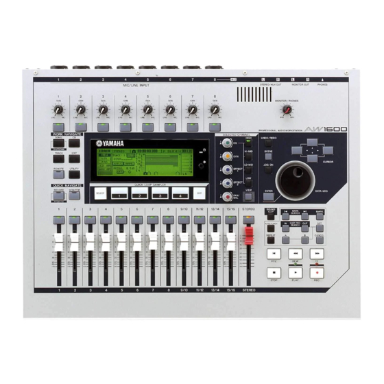
Page 8: Panel Layout
AW1600 ■ PANEL LAYOUT (パネルレイアウト) • Top panel (トップパネル) Data entry/control section Work Navigate section Input/output section Selected Channel section (デー タ エ ン ト リ ー / (ワー ク ナビゲー ト セ ク シ ョ ン) (入出力セ ク シ ョ ン) (セ... - Page 9 AW1600 Work Navigate section ( ワ ー ク ナビ ゲー ト セ ク シ ョ ン) 1 [SONG] key ([SONG] キー) 2 [CD] key ([CD] キー) 3 [TRACK] key ([TRACK] キー) 4 [EDIT] key ([EDIT] キー) 5 [REMOTE] key ([REMOTE] キー) 6 [UTILITY] key ([UTILITY] キー)...
- Page 10 AW1600 Mixer section ( ミ キサーセ ク シ ョ ン) 1 [TRACK SEL] keys 1-8 ([TRACK SEL] キー 1 ~ 8) 4 Faders 1-8 (フ ェ ーダー 1 ~ 8) 2 [TRACK SEL] keys 9/10-15/16 5 Faders 9/10-15/16 (フ ェ ーダー 9/10 ~ 15/16) 6 [STEREO] fader ([STEREO] フ...
- Page 11 AW1600 Locate section ( ロ ケー ト セ ク シ ョ ン) 1 [SOUND CLIP] key ([SOUND CLIP] キー) 2 [AUTO PUNCH] key ([AUTO PUNCH] キー) 3 [REPEAT] key ([REPEAT] キー) 4 MARK SEARCH [ O]/[P] keys (MARK SEARCH [ O]/[P] キー) 5 [IN]/[OUT] keys ([IN]/[OUT] キー)...
-
Page 12: Circuit Board Layout
AW1600 ■ CIRCUIT BOARD LAYOUT (ユニットレイアウト) • Top view (Bottom cover section) CN651 CN652 Hard Disk Drive Assembly CN308 MAIN CN101 CN102 CN309 CD Drive Assembly CN102 CN306 CN402 CN403 CN003 CN006 CN002 CN001 CN003 CN001 CN002 CN004 Hard Disk Drive Assembly CN405 CN104 CN105... - Page 13 AW1600 • Bottom view (Top cover section) CN103 CN102 CN105 CN101 CN003 CN001 CN002 ■ DIMENSIONS (寸法図) Unit: mm (単位)...
- Page 14 AW1600 ■ DISASSEMBLY PROCEDURES ■ 分解手順 • Precautions 注意事項 • フ ィ ラ メ ン ト テープは、 取 り 外す前 と 同 じ よ う に取 り Attach filament tapes in the same as those before removing. 付けて く だ さ い。 Notes on Flat Cable フ...
- Page 15 AW1600 [350] [370] [370] [370] [350] [40] [585] [585] [590] [590] [195] DC Cord Column [245] [240] [190] [180] コードコラム) [590] [40] Bind Head Tapping Screw-S 3x6 MFZN2W3 (WE877900) S タ イ ト + B I N D [180] Hexagonal Nut 12 (V9475600) 特種六角ナ ッ ト [190] Bonding Tapping Screw-B 3x10 MFZN2B3 (WE878000) B...
- Page 16 AW1600 Retainer [550A] ツメ [530] Sheet PN Assembly PN Ass’y) シート Protection Sheet 液晶ディスプレイ 保護シート [550B] LCD Support (LCD サポート Sheet PN Assembly PN Ass’y) シート Pull the retainer section to the front and remove the connector. ツメの部分を手前に引き コネクタを外します。 Retainer ツメ) [530] Bind Head Tapping Screw-B 3x10 MFZN2W3 (WE774200) B...
- Page 17 AW1600 ADA Cricuit Board [375] (ADA シート [340] [150] Shield Angle シールドアングル MAIN Cricuit Board (MAIN シート [150] Bind Head Tapping Screw-S 3x6 MFZN2W3 (WE877900) S タ イ ト + B I N D [340] Bind Head Tapping Screw-S 3x6 MFZN2W3 (WE877900) S タ イ ト + B I N D [375] Bind Head Tapping Screw-S 3x6 MFZN2W3 (WE877900) S...
- Page 18 AW1600 PW Circuit Board PW シー ト (所要時間 : 約 9 分) (Time required: about 9 minutes) ト ッ プカバーを外 し ます。 (1 項参照) ADA シー ト と シール ド ア ン グルを外 し ます。(4項参照) Remove the top cover. (See procedure 1.) [245] のネジ...
- Page 19 AW1600 Hard Disk Drive Assembly, Hard Disk Drive HDD Ass’y、 HDD (所要時間 : 約 5 分) (Time required: about 5 minutes) ト ッ プカバーを外 し ます。 (1 項参照) [40] のネジ 6 本を外 し て、HDD Ass’y を外 し ます。(図 2) Remove the top cover. (See Procedure 1.) [30B] のネジ...
- Page 20 AW1600 Hard Disk Drive Assembly, Hard Disk Drive HDD Ass’y、 HDD <NEW ASSEMBLY> <NEW ASSEMBLY> (所要時間 : 約 5 分) (Time required: about 5 minutes) ト ッ プカバーを外 し ます。 (1 項参照) [40] のネジ 6 本を外 し て、HDD Ass'y を外 し ます。(図 2) Remove the top cover.
-
Page 21: Lsi Pin Description
AW1600 ■ LSI PIN DESCRIPTION (LSI 端子機能表) M66590FP-RB0S (X5423A00) USB Controller..........21 HD6417709SF133BV (X2081A00) CPU .............22 YSS910-V (XV988B00) DSP6 (Digital Signal Processor)........23 YSS919B-HZ (XZ693B00) DSP7 (Digital Signal Processor) .......24 YM3436D-FZ (XG948E00) DIR2 (Digital Format Interface Receiver) ....25 AK5381VT-E2 (X5219A00) ADC (Analog to Digital Converter) ......25 AK4382AVT (X0661A00) DAC (Digital to Analog Converter) ......25 •... - Page 22 AW1600 • HD6417709SF133BV (X2081A00) CPU MAIN: IC002 PIN No. NAME FUNCTION PIN No. NAME FUNCTION CKE/PTK5 CK enable / Port K Mode control RAS3L/PTJ0 RAS address bus / Port J Vcc(RTC) Power supply +1.8 V PTJ1 Port J XTAL2 CASL/PTJ2 CAS address bus / Port J Crystal oscillator EXTAL2...
- Page 23 AW1600 • YSS910-V (XV988B00) DSP6 (Digital Signal Processor) MAIN: IC205 PIN No. NAME FUNCTION PIN No. NAME FUNCTION Power supply (3.3 V) Ground Ground DB13 System master clock input (60 MHz or 30 MHz) DB14 System master clock output (High or 30 MHz) DB15 Vdd5 Power supply (5 V)
- Page 24 AW1600 • YSS919B-HZ (XZ693B00) DSP7 (Digital Signal Processor) MAIN: IC207 PIN No. NAME FUNCTION PIN No. NAME FUNCTION PLLEN PLL enable input (0: PLL unuse, 1: PLL use) SIO32 /TEST Test mode setting (0: TEST, 1: Normal) SIO33 AVss Analog ground SIO34 PLL filter SIO35...
- Page 25 AW1600 • YM3436D-FZ (XG948E00) DIR2 (Digital Format Interface Receiver) MAIN: IC302 NAME FUNCTION NAME FUNCTION DAUX Auxiliary input for audio data RSTN System reset input HDLT Asynchronous buffer operation flag Vdda VCO section power (+5V) DOUT Audio data output CTLN VCO control input N Parity flag output PLL phase comparison output...
-
Page 26: Ic Block Diagram
AW1600 ■ IC BLOCK DIAGRAM (IC ブロック図) • SN74LV244APWR (X3292A00) • NJM2368M(TE1) (X5185A00) • SN75179B(PS) (XT619A00) Octal 3-State Buffer DC-DC Converter Line Driver DIO: IC001 DIO: IC006 DIO: IC002 0 52V U V L O Driver Receiver INPUTS OUTPUTS DIFFERENTIAL INPUT OUTPUTS 0 2V 0 2V <... - Page 27 AW1600 • TC7WU04FU (XQ805A00) • BU2370FV-E2 (X6355A00) Triple Inverter Phase Locked Loop MAIN: IC211 MAIN: IC317 FIN-B OUT VDD LEVEL FIN-A OUT GND SHIFTER VCOE VCO OUT PHASE VCO VDD DVDD DETECTER VCO GND DGND Pmos VCO IN PD OUT Nmos FSEL1 •...
- Page 28 AW1600 • S1F76610M2E010B (X5962A00) DC-DC Converter LCD: IC103 CAP1+ CAP1– OSC1 OSC1 Oscillator N.C. N.C. OSC2 Reference Temperature Voltage Gradient CAP2+ OSC2 Generator Selector CAP2– CAP1– Voltage Multiplier CAP1+ CAP2– Voltage Regulator Voltage Multiplier CAP2+...
-
Page 29: Circuit Boards
AW1600 ■ CIRCUIT BOARDS (シート基板図) ADA Circuit Board (X5633B0)........32 DIO Circuit Board (X5972C0) ........30 IDE Circuit Board (X5972C0) ........29 LCD Circuit Board (X5633B0) ........31 MAIN Circuit Board (X5626B0) .........34 PN Circuit Board (X5632B0) ........38 PW Circuit Board (X6394B0) ........44 Note: See parts list for details of circuit board component parts. 注... - Page 30 AW1600 • DIO Circuit Board to PW-CN002 N.C. to MAIN-CN308 to MAIN-CN104 to MAIN-CN105 CH5-8 CH1-4 OUT/THRU PHANTOM+48V MIDI FOOT SW ON/OFF DIGITAL STEREO Component side (部品側) Pattern side (パターン側) 2NAP-WD95450-1 2NAP-WD95450-2...
- Page 31 AW1600 • LCD Circuit Board to LCD Unit (BACK LIGHT) to MAIN-CN102 Component side (部品側) Pattern side (パターン側) 2NAP-WD39940-1 2NAP-WD39940-2...
- Page 32 AW1600 • ADA Circuit Board to PW-CN001 GAIN 8 GAIN 7 PHONES HI-Z MONITOR STEREO/AUX A’ MIC/LINE INPUT Component side (部品側) B’ Pattern side (パターン側) 2NAP-WD39940-1 2NAP-WD39940-2...
- Page 33 AW1600 to MAIN-CN103 GAIN 5 GAIN 4 GAIN 3 GAIN 2 GAIN 1 A’ MIC/LINE INPUT Component side (部品側) B’ Pattern side (パターン側) 2NAP-WD39940-1 2NAP-WD39940-2...
- Page 34 AW1600 • MAIN Circuit Board Not installed to LCD-CN101 to PN-CN002 Not installed C’ Component side (部品側) 2NAP-WD44680-1...
- Page 35 AW1600 to DIO-CN001 to DIO-CN002 to ADA-CN651 Not installed to PW-CN004 to PN-CN001 to PN-CN003 Not installed C’ Component side (部品側) 2NAP-WD44680-1...
- Page 36 AW1600 • MAIN Circuit Board Pattern side (パターン側) D’ 2NAP-WD44680-2...
- Page 37 AW1600 Pattern side (パターン側) D’ 2NAP-WD44680-2...
- Page 38 AW1600 • PN Circuit Board Component side (部品側) 2NAP-WD39930 to MAIN-CN306 E’...
- Page 39 AW1600 9/10 11/12 13/14 15/16 STEREO 9/10 11/12 13/14 15/16 STEREO 2NAP-WD39930 Component side (部品側) E’ to MAIN-CN402 to MAIN-CN403 F’...
- Page 40 AW1600 STEREO STEREO Component side 2NAP-WD39930 (部品側) F’...
- Page 41 AW1600 • PN Circuit Board 2NAP-WD39930 Pattern side (パターン側) G’...
- Page 42 AW1600 Pattern side 2NAP-WD39930 (パターン側) G’ H’...
- Page 43 AW1600 Pattern side (パターン側) 2NAP-WD39930 H’...
- Page 44 AW1600 • PW Circuit Board to Hard disk drive Component side (部品側) DC IN I’ Pattern side (パターン側) J’ 2NAP-WE74710...
- Page 45 AW1600 to MAIN-CN405 to ADA-CN652 Component side (部品側) ON/STANDBY I’ Pattern side (パターン側) J’ 2NAP-WE74710...
- Page 46 The following screen appears during the update. * DO NOT touch any keys or faders, and DO NOT turn the AW1600 power off during the update. Copyright(c) 2005 YAMAHA BOOT OS: V*.** //// UPDATE OS VERSION //// FIRM OS: V*.** BOOT OS: V1.02...
- Page 47 下記の画面が表示 さ れます。 ※ バージ ョ ン ア ッ プ中はキーやフ ェ ーダーに触れた り 、 電源 を切っ た り し ないで く だ さ い。 AW1600 Copyright(c) 2005 YAMAHA //// UPDATE OS VERSION //// BOOT OS: V*.** BOOT OS: V1.02 <- V*.** FIRM OS: V*.**...
- Page 48 LCD. Install the FIRM OS following the Turn the power on. Hold down the [UTILITY] key as the procedure 3-2. YAMAHA logo appears on the LCD. The version of the installed BOOT OS and FIRM OS appears on the LCD. RECOVERY FIRM OS IS BROKEN...
- Page 49 Input frequency Input level Permissible range (distortion) AW1600 1 kHz –46 dBu 0.2% or less Copyright(c) 2005 YAMAHA BOOT OS: V*.** 8 MIC noise level BUILD DATE 2005/**/** **:**:** Set the INPUT GAIN VR to MAX [MIC]. Permissible range –65 dBV or less...
- Page 50 AW1600 5-2-8 INPUT 8 (BAL XLR) Jitter measurement (1) Measure at INPUT 8 – > MONITOR OUT R. (1) Measure the jitter value of the DIGITAL OUT with the (2) Set the MONITOR/PHONES VR to MAX. DSA-1. (3) The measured item and the value are same as specified 1) WORD CLOCK SOURCE: jitter of 5 nsec or less for INPUT 1.
- Page 51 AW1600 ■ 検査 測定条件 確認方法 通常立ち上げで LCD 画面に下記の メ ッ セージが表示 さ 測定器、 測定治具 れた場合は、 FIRM OS は イ ン ス ト ール さ れてい ません • PC は、 USB2.0 対応 ので 3-2 の手順に従っ て イ ン ス ト ールを行っ て く だ さ •...
- Page 52 バージ ョ ンの確認方法 2-3 ピ ン間を 150Ω でシ ョ ー ト し 、 INPUT 8 (Hi-Z) 端 電源を入れ、LCD に YAMAHA の ロ ゴが表示 さ れた ら 、 子は無入力 と し ます。 [UTILITY] キーを押 し 続け る と イ ン ス ト ール さ れてい...
- Page 53 AW1600 5-2-6 INPUT 6 (BAL XLR) 通常モー ド での検査 (1) INPUT 6 – > MONITOR OUT R にて測定 し ます。 DIGITAL IN (COAXIAL) (2) MONITOR/PHONES VR を MAX に し ます。 (1) 外部か ら の DIGITAL 信号(Fs:44.1kHz –10%、+6%) に (3) 測定項目、 規格値は INPUT 1 と 同様です。 対...
-
Page 54: Test Program
2-2-2 When the following screen appears on the LCD, -06.MIDI -14.W.CLOCK -07.USB -15.SDRAM release the keys. -08.MUTE -16. Result AW1600 Normal: Copyright(c) 2005 YAMAHA Abnormal: BOOT OS: V*.** Canceled: BUILD DATE 2005/**/** **:**:** 2-2-3 The program starts up and the test menu screen appears on the LCD. - Page 55 AW1600 Description of each test 4-2-2 Test content Check the function of the [EQ], [DYN], [EFF1], [EFF2], Test item indication [PAN] and [DATA/JOG] rotary encoders. 4-2-3 Procedures 01. SWITCH The name of the encoder to be tested, the value and the direction of rotation appear on the LCD.
- Page 56 AW1600 4-3-4 Judgment 4-5-1 Display Display Judgment 05. LCD “○” is displayed to the left of The test completes the test item successfully. “×” is displayed to the left of The test fails or is canceled. the test item OK:[ENTER],NG:[CANCEL] LED function test (04.LED) 4-4-1 Display 4-5-2 Test content...
- Page 57 AW1600 If the test completes successfully: B) Check the hard disk drive on AW1600 (AW1600-1 and The test menu screen reappears with “ ” displayed to the AW1600-2) is mounted on the “My Computer” window. left of the test item, and the cursor advances to the next test item.
- Page 58 AW1600 3 Check that no device is displayed and click the “Close” Analog mute test (08.MUTE) button. 4-8-1 Display 08. MUTE Analog Mute ON OK:[ENTER],NG:[CANCEL] 4-8-2 Test content Check whether the analog mute functions correctly. 4-8-3 Procedures Check that the mute function is active while the message “Analog Mute ON”...
- Page 59 AW1600 The test items and the test results are displayed on the LCD. Same as * above. (9) “7:DRAM Interface (Address bus)...NG” is displayed 1: CPU Interface (Data bus 1)...** during the test: (TxBusy test of WCR regist) Same as * above. 2: CPU Interface (Data bus 2)...** 4-10 DSP7 function test (10.DSP7)
- Page 60 AW1600 (3) “1:CPU Interface (Data bus 1)...NG” is displayed during If the test fails or if you wish to cancel the test: the test: Press the [CANCEL] key. The test menu screen reappears MSB 28 with “×” displayed to the left of the test item. If there is any error, the error message is displayed on the IC207 XXXX XXXX XXXX XXXX XXXX XXXX XXXX XXXX LCD.
- Page 61 AW1600 4-12-4 Judgment 4-13-4 Judgment Display Judgment Display Judgment “○” is displayed to the left of The test completes “○” is displayed to the left of The test completes the test item successfully. the test item successfully. “×” is displayed to the left of The test fails or is canceled.
- Page 62 AW1600 4-15 SDRAM (HGA) function test (15.SDRAM) 4-15-1 Display 15. SDRAM OK ! EXIT:[ENTER] 4-15-2 Test content Check the HGA connections. 4-15-3 Procedures This test is executed automatically. If the test completes successfully: The test menu screen reappears with “ ” displayed to the left of the test item (15.SDRAM), and the cursor advances to the next test item.
- Page 63 2-2-2 LCD DISPLAY に下記のよ う に表示 さ れるのでキーか 07.USB 15.SDRAM 08.MUTE ら手を離 し ます。 結果 正常:○ AW1600 Copyright(c) 2005 YAMAHA 異常:× 中断:× BOOT OS: V*.** BUILD DATE 2005/**/** **:**:** テ ス ト プ ロ グ ラ ムが起動 し 検査項目表示画面にな り ま 2-2-3 す。...
- Page 64 AW1600 検査 ENCODER 機能検査 (02.ENCODER) 4-2-1 表示 検査項目名表示部 02. ENCODER 01. SWITCH 0 -> EFF1 EFF2 NG:[CANCEL] NG:[CANCEL] 4-2-2 検査内容 メッセージ表示部 完了・中断指示部 [EQ]、 [DYN]、 [EFF1]、 [EFF2]、 [PAN]、 [JOG] の ロ ー タ リ ーエン コ ーダーの機能を検査 し ます。 ス イ ッ チ入力検査 (01.SWITCH) 4-2-3 検査手順...
- Page 65 AW1600 0 → 127 ま で正常に動作 し た フ ェ ーダーは、 その名 異常 ・ 中断の場合 : 称の左側に * が表示 さ れます。 異常ま たは中断 し たい場合は [CANCEL] キーを押す こ と に よ り 検査項目表示画面に戻 り ま す。 こ の と き 検査 正常の場合...
- Page 66 AW1600 4-6-2 検査内容 2) PC への内蔵 HDD のマ ウ ン ト 及びア ン マ ウ ン ト テ MIDI I/F の機能を検査 し ます。 ス ト A) USB ケーブルを PC に接続 し ます。 4-6-3 検査手順 B) PC の 「マ イ コ ン ピ ュ ー タ 」 で AW1600 内蔵の HDD 接続お...
- Page 67 AW1600 3 何 も デバ イ ス が無い こ と を確認 し 「閉 じ る 」 を ク アナログ ミ ュ ー ト 検査 (08.MUTE) リ ッ ク し ます。 4-8-1 表示 08. MUTE Analog Mute ON OK:[ENTER],NG:[CANCEL] 4-8-2 検査内容 アナ...
- Page 68 AW1600 4-9-2 検査内容 (6) 検査中に 4:CPU Interface (Address bus)...NG と 表示 さ CPU ⇔ DSP6 間お よ び DSP6 ⇔ DRAM 間 イ ン タ ーフ ェ れ る : イ ス検査 ※ と 同一 (7) 検査中に 5:CPU Interface (BUS,W/R,Reg)...NG と 表示 さ...
- Page 69 AW1600 4-10-4 検査判定 正常の場合 : (1) 検査項目欄の左端に○が表示 さ れ る : 正常の場合、 検査項目表示画面に戻 り 、 検査項目欄の 検査が正常に終了 し た 左端に○を表示 し 、 次の検査項目に カー ソ ルが移動 し (2) 検査項目欄の左端に×が表示 さ れ る : ます。 検査が異常終了 も し く は中断 し た (3) 検査中に1:CPU Interface (Data bus 1)...NG と...
- Page 70 AW1600 4-12-4 検査判定 4-13-4 検査判定 表示 判定 表示 判定 検査項目欄の左端に○が表示 検査が正常に終了 し た 検査項目欄の左端に○が表示 検査が正常に終了 し た さ れる さ れる 検査項目欄の左端に×が表示 検査が異常終了も し く は中断 検査項目欄の左端に×が表示 検査が異常終了 も し く は中断 さ れる し た さ れる し た 検査中に...
- Page 71 AW1600 SDRAM (HGA) 機能検査 (15.SDRAM) 4-15 4-15-1 表示 15. SDRAM OK ! EXIT:[ENTER] 4-15-2 検査内容 HGA に関す る 接続検査 4-15-3 検査手順 自動で実行 さ れ る ので操作の必要はあ り ません。 正常の場合 : 正常の場合、 検査項目表示画面に戻 り 、 検査項目欄の 左端に○ を表示 し 、 次の検査項目にカー ソ ルが移動 し ます。...
-
Page 72: Initializing The Internal Hard Disk
AW1600 ■ RESTORING THE INTERNAL HARD DISK TO THE FACTORY-SET CONDITION In order to restore the internal hard disk to the factory-set Make sure that the cursor is located at the condition, you will need to perform the following two pro- READ CD INFO button, and press the cedures. - Page 73 AW1600 ■ 内蔵ハードディスクを工場出荷時の設定に戻す 内蔵ハードディスクを工場出荷時の設定に戻すためには、大 READ CD INFO ボタンにカーソルがあることを確認し、 きく分けて次の2つの作業が必要になります。 [ENTER]キーを押します。 CD-ROMの読み出しが始まります。読み出しが終わると 1 内蔵ハードディスクの初期化 ページの表示が次のように変わります。 2 デモソング、サンプルライブラリーの読み出し 内蔵ハードディスクの初期化 内蔵ハードディスクを初期化すると、システム設定が工場出 荷時の状態に戻ります。 UTILITY画面のD.IN HDDページを呼び出すには、ワークナビ DISABLEボタンにカーソルを合わせ、[ENTER]キーを ゲートセクションの[UTILITY] キーを繰り返し押すか、 押します。 [UTILITY] キーを押しながらCURSOR[3]/[4] キーを押しま DISABLEボタンの表示がENABLE に変わり、リストの す。 右端のマークが“●”に変わります。 FORMAT ボタン PADボタンにカーソルを合わせ、[ENTER]キーを押します。 再びCD-ROMの読み出しが始まります。読み出しが終わ るとページの表示が次のように変わります。 FORMATボタン 内蔵ハードディスクを初期化します。ボタンにカーソルを合 わせて [ENTER] キーを押すと、初期化を実行します。実行 中は進行状況を示すポップアップウィンドウが表示されます。...
-
Page 74: Display Message List
AW1600 ■ DISPLAY MESSAGE LIST • Messages A/B POINTS NOT FOUND Repeat Playback cannot be performed because A/B points are not specified. CANNOT DEFEAT MUTE Mute cannot be disengaged because the simultaneous playback limit will be exceedced. CANNOT REDO! Redo (re-execution of an operation) is not possible. CANNOT SET MARK It is not possible to specify a mark at an already-specified position. -
Page 75: Popup Messages
AW1600 • Popup messages ALL Song Data Corrupt! Format INT.HDD. The file system is corrupt. The internal hard disk will be initialized. Audio Data Too Short! The sample is too short. Buffer Underrun! A buffer underrun error was encountered while writing to the CD. CD Import Prohibited! Enable DIGITAL REC. - Page 76 AW1600 Wav File Link Error! Delete Wrong Data? A portion of the song data is corrupt. Erase the corrupt data? If you move the cursor to the OK button and press the [ENTER] key, the corrupt portion of the song will be erased. If you move the cursor to the CANCEL button and press the [ENTER] key, another song will be loaded instead.
- Page 77 AW1600 ■ ディスプレイメッセージリスト • メッセージ A/B POINTS NOT FOUND A/B ポ イ ン ト が設定 さ れていないため、 リ ピー ト 再生を行なえ ません。 CANNOT DEFEAT MUTE 再生 ト ラ ッ ク数の制限を超え るので、 ミ ュ ー ト を解除で き ません。 リ ド ゥ ( 操作の再実行 ) がで き ません。 CANNOT REDO! CANNOT SET MARK 既に設定...
- Page 78 AW1600 • ポップアップメッセージ ALL Song Data Corrupt! Format INT.HDD. フ ァ イルシ ス テムが壊れてい るので、 内蔵ハー ド デ ィ ス ク を初期化 し ます。 サン プルの長 さ が短すぎ ます。 Audio Data Too Short! Buffer Underrun! CD への書き込み時に、 バ ッ フ ァ ーア ン ダー ラ ンが発生 し ま し た。 CD Import Prohibited! Enable DIGITAL REC.
- Page 79 AW1600 Wav File Link Error! Delete Wrong Data? ソ ングデー タ の一部が壊れているので、 壊れている部分を削除 し ますか? OK ボ タ ンに カ ー ソルを合 わせて [ENTER] キーを押す と 、 壊れている部分を削除 し て ソ ングを読み込みます。 CANCEL ボ タ ン に カ ー ソルを合わせて [ENTER] キーを押す と 、 正常な別の ソ ングを読み込みます。 Wave File Link Error! WAV フ...
- Page 80 AW1600 ■ MIDI INPLEMENTATION CHART YAMAHA [ Professional Audio Workstation ] Date :21-JUL-2004 Model AW1600 MIDI Implementation Chart Version : 1.0 Transmitted Recognized Remarks Function... Basic Default 1 - 16 1 - 16 Memorized Channel Changed 1 - 16 1 - 16...
-
Page 81: Midi Data Format
AW1600 ■ MIDI DATA FORMAT 1. Functions 2. MIDI data flow diagram 1.1. Scene Change The settings of the [MIDI PROGRAM CHANGE TABLE] specify MTC SLAVE USB-1 IN MTC (MTC Slave) the scene that is recalled when a Program Change message is USB-2 IN EFF MIDI received. - Page 82 AW1600 3.1.9. MTC SYNC AVERAGE 5. MIDI format details When the AW1600 is functioning as a MTC SLAVE, this setting 5.1. NOTE OFF (8n) specifies how it will follow the MTC data. Set this to 0 if the incom- < Reception > ing MTC data has a highly accurate timing;...
- Page 83 AW1600 5.5. MIDI TIME CODE QUARTER FRAME (F1) 5.13. EXCLUSIVE MESSAGE (F0-F7) < Transmission > 5.13.1. MMC If [MIDI OUT] is set to MTC, Quarter Frame messages will be trans- 5.13.1.1. MMC STOP mitted according to the time code movements of the recorder when <...
- Page 84 AW1600 5.13.1.5. MMC REWIND 5.13.1.9. MMC LOCATE (TARGET) < Transmission > < Transmission > This message is transmitted with a device number of 7F when the This message is transmitted with a device number of 7F when a REWIND key is pressed. locate-related key such as MARK SEARCH/IN/OUT is pressed, a FF/REW operation is performed, when the transport returns to the <...
-
Page 85: Parts List
AW1600 PROFESSIONAL AUDIO WORKSTATION PARTS LIST ■ CONTENTS (目次) OVERALL ASSEMBLY (総組立).......................2 CD DRIVE ASSEMBLY (CD ド ラ イ ブ Ass’y)..................5 HARD DISK DRIVE ASSEMBLY (HDD Ass’y) .................6 HARD DISK DRIVE ASSEMBLY (HDD Ass’y) <NEW ASSEMBLY> ....... 7 ELECTRICAL PARTS (電気部品) ......................8 Notes : DESTINATION ABBREVIATIONS Australian model South African model... -
Page 86: Overall Assembly
AW1600 ■ OVERALL ASSEMBLY (総組立) Sheet PN Assembly(シートPN Ass’y) 470d 470e 470c 470f 470d 470b 470c 470e 470i 470a 470d 470k 470h 470j 470g 470l Sheet PN Assembly PN Ass’y シート • Accessories (付属品) AC Adaptor(ACアダプター) * This figure shows Japanese model. * この図は日本モデルです。... - Page 87 AW1600 部 品 名 REF NO. PART NO. DESCRIPTION REMARKS QTY RANK OVERALL ASSEMBLY AW1600 (WE15160) 総 組 立 Bottom Cover WE138600 ボ ト ム カ バ ー 印 刷 上 り Leg Banpon CLEAR SJ-1005CH レ ッ グ バ ン ポ ン WF622000 Hard Disk Drive Assembly H...
- Page 88 AW1600 部 品 名 REF NO. PART NO. DESCRIPTION REMARKS QTY RANK 470f Button Black SONG/SHUT DOWN <WORK NAVIGATE> WD400200 ボ タ ン L <WORK NAVIGATE> TRACK <WORK NAVIGATE> EDIT <WORK NAVIGATE> UTILITY <WORK NAVIGATE> 470g Button White PLAY ボ タ ン T R P L A Y PLAY WE207900 470h...
- Page 89 AW1600 ■ CD DRIVE ASSEMBLY (CD ドライブ Ass’y) 部 品 名 REF NO. PART NO. DESCRIPTION REMARKS QTY RANK CD DRIVE ASSEMBLY C D ド ラ イ ブ A s s’ y AW1600 (WE15270) DVD & CD-R/W Drive UJDA760YA-A D V D & C D - R / W WE213600 Support, CDRW サ...
- Page 90 AW1600 ■ HARD DISK DRIVE ASSEMBLY (HDD Ass’y) 部 品 名 REF NO. PART NO. DESCRIPTION REMARKS QTY RANK HARD DISK DRIVE ASSEMBLY AW1600 (WE22420) H D D A s s’ y Hard Disk Drive ST340014A 40G WE213800 H D D 3 5 - 4 0 G M HDD Cover WE140300 H...
- Page 91 AW1600 ■ HARD DISK DRIVE ASSEMBLY (HDD Ass’y) <NEW ASSEMBLY> 部 品 名 REF NO. PART NO. DESCRIPTION REMARKS QTY RANK HARD DISK DRIVE ASSEMBLY AW1600 (WE22420) H D D A s s’ y Hard Disk Drive ST340014A 40G WE213800 H...
-
Page 92: Electrical Parts
AW1600 ■ ELECTRICAL PARTS (電気部品) 部 品 名 REF NO. PART NO. DESCRIPTION REMARKS QTY RANK ELECTRICAL PARTS AW1600 電 気 部 品 Circuit Board DIO (DIOCOM 1/2) (WD95450)(X5972C0) WE211900 D I O シ ー ト Circuit Board IDE (DIOCOM 2/2) I... - Page 93 AW1600 部 品 名 REF NO. PART NO. DESCRIPTION REMARKS QTY RANK JK001 Phone Jack Black YKB21-5244 FOOT SW VY695400 ホ ー ン コ ネ ク タ (黒) JK002 DIN Connector 5P3 HDC-052A MIDI (IN,OUT/THRU) V6177500 D I N コ ネ ク タ 2 連 JK002 DIN Connector YKF51-5058N...
- Page 94 AW1600 部 品 名 REF NO. PART NO. DESCRIPTION REMARKS QTY RANK C004 Ceramic Capacitor-F(chip) 25V Z US145100 チ ッ プ セ ラ (F) -008 Ceramic Capacitor-F(chip) 25V Z US145100 チ ッ プ セ ラ (F) C009 Electrolytic Cap. (chip) 6.3V チ...
- Page 95 AW1600 部 品 名 REF NO. PART NO. DESCRIPTION REMARKS QTY RANK -321 Ceramic Capacitor-F(chip) 25V Z US145100 チ ッ プ セ ラ (F) C326 Ceramic Capacitor-F(chip) 25V Z US145100 チ ッ プ セ ラ (F) C328 Ceramic Capacitor-F(chip) 25V Z チ...
- Page 96 AW1600 部 品 名 REF NO. PART NO. DESCRIPTION REMARKS QTY RANK * IC014 MX29LV800CBTC-70G FLASH ROM 8M MAIN X6543D00 I C IC015 SN74LV11APWR X3516A00 I C IC101 SN74LVCC4245APWR I C TRANSCEIVER X3096A00 IC102 SN74LVCC4245APWR I C TRANSCEIVER X3096A00 IC103 SN74AHCT245PWR I...
- Page 97 AW1600 部 品 名 REF NO. PART NO. DESCRIPTION REMARKS QTY RANK R305 Carbon Resistor (chip) 1/16W J RD354220 チ ッ プ 抵 抗 -307 Carbon Resistor (chip) 1/16W J RD354220 チ ッ プ 抵 抗 R309 Carbon Resistor (chip) 1/16W J チ...
- Page 98 AW1600 部 品 名 REF NO. PART NO. DESCRIPTION REMARKS QTY RANK RA038 Resistor Array 22x4 RE044220 抵 抗 ア レ イ -045 Resistor Array 22x4 RE044220 抵 抗 ア レ イ RA054 Resistor Array 22x4 抵 抗 ア レ イ...
- Page 99 AW1600 部 品 名 REF NO. PART NO. DESCRIPTION REMARKS QTY RANK * LD029 LED Red/Green SML72423C TP15 (TRACK SELECT) 7 WF636600 L E D 2 色 * LD030 LED Red/Green SML72423C TP15 (TRACK SELECT) 8 WF636600 L E D 2...
- Page 100 AW1600 部 品 名 REF NO. PART NO. DESCRIPTION REMARKS QTY RANK SW029 Push Switch EVQ 11Y 05B (TRACK SELECT) 7 V8889400 プ ッ シ ュ S W SW029 Tact Switch SKQNAED010 VV056000 タ ク ト S W SW030 Push Switch EVQ 11Y 05B プ...
- Page 101 AW1600 部 品 名 REF NO. PART NO. DESCRIPTION REMARKS QTY RANK VR001 Slide Variable Resistor B10K 45mm RS45111A (FADER) 1 V8847000 ス ラ イ ド V R VR002 Slide Variable Resistor B10K 45mm RS45111A (FADER) 2 V8847000 ス ラ イ...
- Page 102 AW1600 部 品 名 REF NO. PART NO. DESCRIPTION REMARKS QTY RANK -003 LC Filter 6NE32A222Q93A WA049400 L C フ ィ ル タ ー E M I EM004 LC Filter 6NF31C223Q93A VD542700 L C フ ィ ル タ ー E M I EM005 LC Filter 6NF31C223Q93A...
- Page 103 AW1600 部 品 名 REF NO. PART NO. DESCRIPTION REMARKS QTY RANK C220 Electrolytic Cap. UU247470 ケ ミ コ ン F W C221 Ceramic Capacitor-F(chip) 25V Z US145100 チ ッ プ セ ラ (F) C222 Electrolytic Cap. ケ ミ コ ン...
- Page 104 AW1600 部 品 名 REF NO. PART NO. DESCRIPTION REMARKS QTY RANK C381 Electrolytic Cap. UU247470 ケ ミ コ ン F W C382 Electrolytic Cap. UU247470 ケ ミ コ ン F W C401 Electrolytic Cap. ケ ミ コ ン UR878100 C402 Ceramic Capacitor-SL(chip) 220P 50V...
- Page 105 AW1600 部 品 名 REF NO. PART NO. DESCRIPTION REMARKS QTY RANK C530 Electrolytic Cap. UU247470 ケ ミ コ ン F W -532 Electrolytic Cap. UU247470 ケ ミ コ ン F W C552 Ceramic Capacitor-SL(chip) 220P 50V チ ッ プ セ ラ (S L) US062220 C553 Ceramic Capacitor-SL(chip)
- Page 106 AW1600 部 品 名 REF NO. PART NO. DESCRIPTION REMARKS QTY RANK C821 Ceramic Capacitor-CH(chip) 50V D US061100 チ ッ プ セ ラ (C H) C823 Electrolytic Cap. UR838330 ケ ミ コ ン C825 Ceramic Capacitor-SL(chip) 470P 50V J チ ッ プ セ ラ (S L) US062470 C826 Electrolytic Cap.
- Page 107 AW1600 部 品 名 REF NO. PART NO. DESCRIPTION REMARKS QTY RANK JK201 Cannon Connector NCJ6FI-H-0 MIC/LINE INPUT 1 V2910100 キ ャ ノ ン コ ネ ク タ JK251 Cannon Connector NCJ6FI-H-0 MIC/LINE INPUT 2 V2910100 キ ャ ノ ン コ ネ ク タ JK301 Cannon Connector NCJ6FI-H-0...
- Page 108 AW1600 部 品 名 REF NO. PART NO. DESCRIPTION REMARKS QTY RANK R203 Carbon Resistor (chip) 820K 1/16W J RD358820 チ ッ プ 抵 抗 R204 Carbon Resistor (chip) 820K 1/16W J RD358820 チ ッ プ 抵 抗 R205 Metal Film Resistor 6.8K 1/4W F 金...
- Page 109 AW1600 部 品 名 REF NO. PART NO. DESCRIPTION REMARKS QTY RANK R356 Metal Film Resistor 6.8K 1/4W F HB026680 金 属 被 膜 抵 抗 R357 Carbon Resistor (chip) 3.3K 1/16W J RD356330 チ ッ プ 抵 抗 R358 Carbon Resistor (chip) 3.3K 1/16W J チ...
- Page 110 AW1600 部 品 名 REF NO. PART NO. DESCRIPTION REMARKS QTY RANK R514 Carbon Resistor (chip) 1/16W J RD357330 チ ッ プ 抵 抗 R515 Carbon Resistor (chip) 1/16W J RD355100 チ ッ プ 抵 抗 R518 Carbon Resistor (chip) 1/16W J チ...
- Page 111 AW1600 部 品 名 REF NO. PART NO. DESCRIPTION REMARKS QTY RANK R763 Carbon Resistor (chip) 1/16W J RD355100 チ ッ プ 抵 抗 R764 Carbon Resistor (chip) 1/16W J RD354510 チ ッ プ 抵 抗 R765 Carbon Resistor (chip) 1/16W J チ...
- Page 112 AW1600 部 品 名 REF NO. PART NO. DESCRIPTION REMARKS QTY RANK TH101 Thermistor(chip) NCP18WF104J03RB V7962300 チ ッ プ サ ー ミ ス タ TR101 Transistor(chip) 2SA1576A T106 TP VR936300 チ ッ プ ト ラ ン ジ ス タ TR102 Transistor 2SC2412K Q,R,S TP ト...
-
Page 113: Circuit Diagram
AW1600 PROFESSIONAL AUDIO WORKSTATION CIRCUIT DIAGRAM ■ CONTENTS (目次) BLOCK DIAGRAM (ブ ロ ッ ク ダ イ アグ ラ ム) ............. 3 SOFTWARE BLOCK DIAGRAM ( ソ フ ト ウ ェ ア ブ ロ ッ ク ダ イ アグ ラ ム) ..4 CIRCUIT DIAGRAM (回路図)... -
Page 114: Block Diagram
■ BLOCK DIAGRAM (ブロックダイアグラム) AW1600 MAIN 48V 1 DSP BLOCK GAIN1 +12A VR201 IC202 (8P) 1 6 20 1 6 20 IC201 / RESADA 4Mbit 4Mbit (8P) IC210 X201 JK201 JK201 DRAM DRAM GAIN2 (14P) +12A 30MHz AK5381VTP VR251 IC202 IC202 IC201 CN103... - Page 115 ■ SOFTWARE BLOCK DIAGRAM (ソフトウェアブロックダイアグラム) AW1600 [MIC/LINE INPUT] METER INPUT 1(...8) INSERT METER LEVEL BAL PHANTOM STEREO L +48V INSERT 4BAND EQ NAMICS (CH1-4/CH5-8) LEVEL METER METER INPUT 4BAND EQ NAMICS (EQ) STEREO R COMBO PRE/POST 4BAND EQ METER NAMICS METER CD PLAY GAIN...
- Page 116 ■ ADA CIRCUIT DIAGRAM 002 (AW1600) AW1600 to PW-CN001 to MAIN-CN103 (Page 16:B1) (Page 11:B11) TRANSCEIVER TRANSCEIVER REGULATOR +12V REGULATOR +5V • NJM78M12DL1ATE1 (X2600A00) REGULATOR +12V 1: INPUT 2: GND 3: OUTPUT 4: GND • NJM78M05DL1A(TE1) (XS534A00) REGULATOR +5V 1: INPUT 2: GND 3: OUTPUT ( セ...
- Page 117 ■ ADA CIRCUIT DIAGRAM 003 (AW1600) AW1600 ( セ ) : Ceramic Capacitor ( セラミックコンデンサ ) ( マ ) : Myler Capacitor ( マイラーコンデンサ ) Not installed ( 未実装 ) OP AMP STEREO/ AUX OUT OP AMP OP AMP MONITOR MONITOR/PHONES OP AMP OP AMP...
- Page 118 ■ DIO CIRCUIT DIAGRAM (AW1600) AW1600 FOOT SW to MAIN-CN105 (Page 11:B16) BUFFER Photo Coupler PHANTOM +48V ON/OFF MIDI OUT/ CH1-4 CH5-8 THRU DC-DC CONVERTER to PW-CN002 INVERTER (Page 16:B2) N.C. DIGITAL STEREO LINE DRIVER ※ Alternate part: Mount one of the two parts shown above, which are different to each other in size.
- Page 119 ■ IDE CIRCUIT DIAGRAM (AW1600) AW1600 to Hard Disk Drive to CD-RW Drive to MAIN-CN309 (Page 13:B10) Not installed ( 未実装 ) Note: See parts list for details of circuit board component parts. 注:シートの部品詳細はパーツリストをご参照ください。 ■ IDE CIRCUIT DIAGRAM (AW1600) Note: Nonpolar capacitors without indications are ceramic capacitors. 注:指示なき無極性コンデンサはセラミックコンデンサです。...
- Page 120 ■ LCD CIRCUIT DIAGRAM (AW1600) AW1600 OP AMP DC-DC CONVERTER to MAIN-CN102 (Page 11:B8) CONTRAST to LCD back light unit to LCD unit to LCD unit Not installed ( 未実装 ) Note: See parts list for details of circuit board component parts. 注:シートの部品詳細はパーツリストをご参照ください。...
- Page 121 ■ MAIN CIRCUIT DIAGRAM 001 (AW1600) AW1600 SYSTEM RESET • µPC2918T-E1(X2157A00) REGULATOR +1.8V Not installed 1: INPUT 2: GND 3: OUTPUT 4: GND SDRAM 64M REGULATOR +1.8V CPU (SH3) SDRAM 64M FLASH ROM 8M TRANSCEIVER TRANSCEIVER TRANSCEIVER TRANSCEIVER TRANSCEIVER Note: See parts list for details of circuit board component parts. ( セ...
- Page 122 ■ MAIN CIRCUIT DIAGRAM 002 (AW1600) AW1600 TRANSCEIVER TRANSCEIVER to LCD-CN101 (Page 9:J2) to ADA-CN651 (Page 5:J1) to DIO-CN002 (Page 7:U9) Not installed ( 未実装 ) Note: See parts list for details of circuit board component parts. CPU/IF 注:シートの部品詳細はパーツリストをご参照ください。 Note: Nonpolar capacitors without indications are ceramic capacitors. ■...
- Page 123 ■ MAIN CIRCUIT DIAGRAM 003 (AW1600) AW1600 DRAM 4M DSP6 DSP7 INVERTER DRAM 4M D-FF REGULATOR +2.5V • µPC2925T-E1(X0637A00) REGULATOR +2.5V 1: INPUT 2: GND 3: OUTPUT 4: GND ( セ ) : Ceramic Capacitor ( セラミックコンデンサ ) ( マ ) : Myler Capacitor ( マイラーコンデンサ ) (D) : Metal Film Resistor(金属被膜抵抗)...
- Page 124 ■ MAIN CIRCUIT DIAGRAM 004 (AW1600) AW1600 ( セ ) : Ceramic Capacitor ( セラミックコンデンサ ) ( マ ) : Myler Capacitor ( マイラーコンデンサ ) • PQ015EZ1HZPH(X6060A00) REGULATOR +1.5V ( フ ) : Film Capacitor ( フィルムコンデンサ ) (D) : Metal Film Resistor(金属被膜抵抗)...
- Page 125 ■ MAIN CIRCUIT DIAGRAM 005 (AW1600) AW1600 LED DRIVER to PN-CN001 (Page 15:T2) to PN-CN003 (Page 15:M2) INVERTER to PW-CN004 (Page 16:B5) ( セ ) : Ceramic Capacitor ( セラミックコンデンサ ) Not installed ( 未実装 ) Note: See parts list for details of circuit board component parts. 注:シートの部品詳細はパーツリストをご参照ください。...
- Page 126 ■ PN CIRCUIT DIAGRAM (AW1600) AW1600 to MAIN-CN403 (Page 14:C7) to MAIN-CN402 (Page 14:C5) EFFECT 1 EFFECT 2 PAN/BAL DATA/JOG ( セ ) : Ceramic Capacitor ( セラミックコンデンサ ) Note: See parts list for details of circuit board component parts. 注:シートの部品詳細はパーツリストをご参照ください。...
- Page 127 ■ PW CIRCUIT DIAGRAM (AW1600) AW1600 POWER ON/STANDBY to ADA-CN652 (Page 5:E1) DC IN to DIO-CN006 (Page 7:J6) REGULATOR +12V to Hard Disk Drive ( セ ) : Ceramic Capacitor ( セラミックコンデンサ ) ( マ ) : Myler Capacitor ( マイラーコンデンサ ) (D) : Metal Film Resistor(金属被膜抵抗)...
Need help?
Do you have a question about the AW-1600 and is the answer not in the manual?
Questions and answers