Yamaha A-S500 Service Manual
Hide thumbs
Also See for A-S500:
- Owner's manual (154 pages) ,
- Owner's manual (42 pages) ,
- Owner's manual (38 pages)
Table of Contents
Advertisement
A-S500/A-S300
This manual has been provided for the use of authorized YAMAHA Retailers and their service personnel.
It has been assumed that basic service procedures inherent to the industry, and more specifi cally YAMAHA Products, are already known
and understood by the users, and have therefore not been restated.
WARNING:
IMPORTANT:
The data provided is believed to be accurate and applicable to the unit(s) indicated on the cover. The research, engineering, and service
departments of YAMAHA are continually striving to improve YAMAHA products. Modifications are, therefore, inevitable and
specifi cations are subject to change without notice or obligation to retrofi t. Should any discrepancy appear to exist, please contact the
distributor's Service Division.
WARNING:
IMPORTANT:
■ CONTENTS
To Service Personnel ............................................2
Impedance Selector ...............................................3
Front Panels .............................................................3
Rear Panels ...........................................................4–8
Remote Control Panel ..........................................9
SPECIFICATIONS / 参考仕様 ................................... 9–10
Internal View .......................................................... 11
SERVICE PRECAUTIONS / サービス時の注意事項 ..... 11
DISASSEMBLY PROCEDURES / 分解手順 ........... 12–15
ファームウェアの書き込み ..................................... 16–20
1 0 1 1 8 8
INTEGRATED AMPLIFIER
SERVICE MANUAL
IMPORTANT NOTICE
Failure to follow appropriate service and safety procedures when servicing this product may result in personal injury,
destruction of expensive components, and failure of the product to perform as specifi ed. For these reasons, we advise
all YAMAHA product owners that any service required should be performed by an authorized YAMAHA Retailer or
the appointed service representative.
The presentation or sale of this manual to any individual or fi rm does not constitute authorization, certifi cation or
recognition of any applicable technical capabilities, or establish a principle-agent relationship of any form.
Static discharges can destroy expensive components. Discharge any static electricity your body may have
accumulated by grounding yourself to the ground buss in the unit (heavy gauge black wires connect to this buss).
Turn the unit OFF during disassembly and part replacement. Recheck all work before you apply power to the unit.
SELF-DIAGNOSTIC FUNCTION /
ダイアグ(自己診断機能) .......................................21–27
AMP ADJUSTMENT / アンプ部調整 .......................28–29
Ic Data ...................................................................30–32
Pin Connection Diagrams .............................33–34
Block Diagram ........................................................35
Printed Circuit Boards .................................36–52
Schematic Diagrams .......................................53–61
Replacement Parts List ................................63–79
REMOTE CONTROL .....................................................80
Copyright © 2010
This manual is copyrighted by YAMAHA and may not be copied or
redistributed either in print or electronically without permission.
All rights reserved.
P.O.Box 1, Hamamatsu, Japan
'10.09
Advertisement
Table of Contents

Related Manuals for Yamaha A-S500


Summary of Contents for Yamaha A-S500
-
Page 1: Integrated Amplifier
This manual has been provided for the use of authorized YAMAHA Retailers and their service personnel. It has been assumed that basic service procedures inherent to the industry, and more specifi cally YAMAHA Products, are already known and understood by the users, and have therefore not been restated. -
Page 2: To Service Personnel
0.15 μF. ties. For U model “CAUTION” “F1: FOR CONTINUED PROTECTION AGAINST RISK OF FIRE, REPLACE ONLY WITH SAME TYPE 8A (A-S500) / 6A (A-S300), 125V FUSE.” For C model CAUTION REPLACE WITH SAME TYPE 8A (A-S500) / 6A (A-S300), 125V FUSE. -
Page 3: Impedance Selector
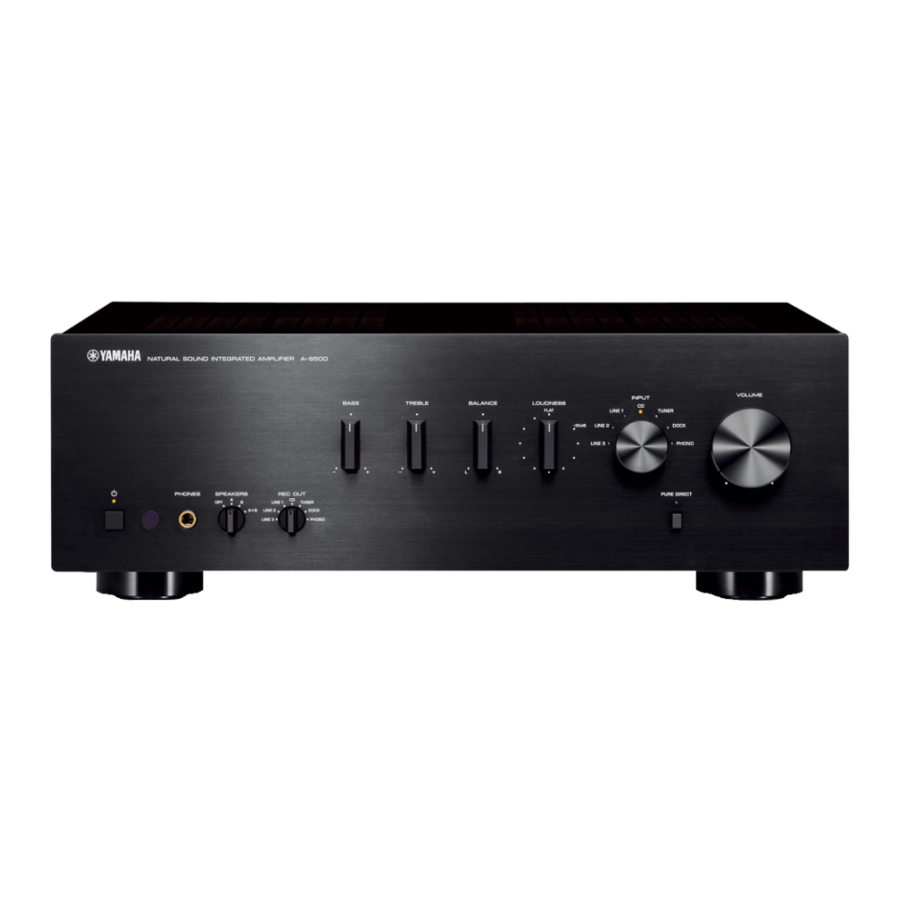
IMPEDANCE SELECTOR ■ FRONT PANELS A-S500 A-S500 (U, C, R, T, A, B, G, L models) A-S300 A-S300 (R, T, A, B, G, L, J models) -
Page 4: Rear Panels
A-S500/A-S300 ■ REAR PANELS A-S500 A-S500 (U, C models) A-S500 (R model) A-S500 (T model) - Page 5 A-S500/A-S300 A-S500 A-S500 (A model) A-S500 (B model) A-S500 (G model)
- Page 6 A-S500/A-S300 A-S500 A-S500 (L model) A-S300 A-S300 (R model) A-S300 (T model)
- Page 7 A-S500/A-S300 A-S300 A-S300 (A model) A-S300 (B model) A-S300 (G model)
- Page 8 A-S500/A-S300 A-S300 A-S300 (L model) A-S300 (J model)
- Page 9 (6 ohms, 20 Hz to 20 kHz, 0.038 % THD) [A-S500] (U, C, R, T, A, B, G models) ..100 W + 100 W [A-S300] (U, C, R, T, A, B, G, J models) ..70 W + 70 W Dynamic Power Per Channel / ダイナミックパワー...
- Page 10 ................1.2 W or less 335 (13-1/4") iPod Charge Power Consumption / iPod 充電時消費電力 (2") [A-S500] ..............35 W or less [A-S300] ..............25 W or less Maximum Power Consumption [R model] Front view (1 kHz, 6 ohms, 10 % THD) [A-S500] ................510 W...
-
Page 11: Internal View
A-S500/A-S300 ■ INTERNAL VIEW A-S500 A-S300 Top view OPERATION (1) P.C.B. MAIN (6) P.C.B. MAIN (5) P.C.B. (J model) OPERATION (7) P.C.B. (R model) MAIN (2) P.C.B. DOCK P.C.B. FUNCTION (2) P.C.B. FUNCTION (3) P.C.B. FUNCTION (1) P.C.B. MAIN (4) P.C.B. -
Page 12: Disassembly Procedures
Remove the top cover. (Fig. 1) b. トップカバーを取り外します。 (Fig. 1) 2. Removal of Front Panel Unit 2. フロントパネルユニットの外し方 a. (A-S500) a. (A-S500) Remove screw ( ④ ), screw ( ⑤ ) and then remove the ④ のネジ 1 本、⑤ のネジ 1 本を外し、フレーム TOP frame top. - Page 13 A-S500/A-S300 3. Removal of Sub-chassis Unit 3. サブシャーシユニットの外し方 a. Remove 2 screws ( ⑧ ). (Fig. 2) a. ⑧ のネジ 2 本を外します。 (Fig. 2) b. Remove CB101, CB108, CB503-505, CB706, CB851 b. CB101、CB108、CB503 ∼ 505、CB706、CB851、 and CB853-854. (Fig. 2) CB853 ∼ 854 を外します。 (Fig. 2)...
- Page 14 A-S500/A-S300 When checking the P.C.B.s: P.C.B. をチェックする場合には: • Put the rubber sheet and cloth over this unit. Then ・ 本機の上にゴムシートと布を敷き、その上にサブ place the sub-chassis unit on the cloth and check it. シャーシユニットを置いてチェックします。 (Fig. 4) (Fig. 4) ・ サ ブ シ ャ ー シ ユ ニ ッ ト の ア ー ス を リ ー ド 線 等 で...
- Page 15 A-S500/A-S300 When checking the MAIN (1) P.C.B.: MAIN(1)P.C.B. をチェックする場合には: • Spread the rubber sheet and the cloth. Then place ・ ゴムシートと布を敷き、 本機を上下反転して置きます。 this unit on the cloth upside down. (Fig. 5) (Fig. 5) • Remove 6 screws ( ⑫ ) and then remove the chassis ・...
-
Page 16: Updating Firmware
A-S500/A-S300 ■ UPDATING FIRMWARE / ファームウェアの書き込み A-S500 A-S300 When the following parts are replaced, the firmware must 下記の部品を交換した場合、ファームウェアを最新バー be updated to the latest version. ジョンにアップデートする必要があります。 FUNCTION P.C.B. FUNCTION P.C.B. Microprocessor (IC502: FUNCTION P.C.B.) Microprocessor (IC502:FUNCTION P.C.B.) ● Confirmation of firmware version ●... - Page 17 A-S500/A-S300 ● Preparation and precautions ● 準備と注意 • Download the firmware downloader program and ・ 指定のダウンロード先から、ファームウェア書き the latest firmware from the specified download 込み用プログラムと最新のファームウェアを、PC source to the same folder of the PC. の同じフォルダにダウンロードしてください。 • Prepare the above specified RS-232C cross ・...
-
Page 18: Operation Procedure
A-S500/A-S300 ● Operation procedure ● 操作方法 1. Connect the power cable of this unit to the AC 1. 本機の電源コードを AC コンセントに接続します。 outlet. 本機に電源が入り、マイコンが書き込みモードに The power to this unit is supplied and the なります。 microprocessor is in the writing mode. 2. FlashSta.exe を起動します。... - Page 19 A-S500/A-S300 5. Click [Setting], and set the baud rate. (Fig. 4) 5. [Setting]をクリックし、通信速度の設定を行い ます。 (Fig. 4) 115200 Fig. 4 6. Click [E.P.R.], then the “Erase” screen appears. (Fig. 5) 6. [E.P.R]をクリックすると、 「Erase」が表示されま す。 (Fig. 5) 7. Click [OK] to start writing. (Fig. 5) 7.
- Page 20 A-S500/A-S300 8. When writing of the firmware is completed, the 8. ファームウェアの書き込みが完了すると、以下の screen appears as shown below. (Fig. 6) 画面が表示されます。 (Fig. 6) Click [OK]. (Fig. 6) [OK]をクリックします。 (Fig. 6) 9. Click [Exit] to end FlashSta.exe. (Fig. 6) 9. [Exit] をクリックして FlashSta.exe を終了します。...
- Page 21 A-S500/A-S300 ■ SELF-DIAGNOSTIC FUNCTION / ダイアグ(自己診断機能) A-S500 A-S300 This unit has self-diagnostic functions that provides the 本機には下記の機能をもつダイアグ(自己診断機能)が following functions. あります。 • Indication of firmware version ・ ファームウェアのバージョン表示 • Indication of power management switch status ・ POWER MANAGEMENT スイッチの状態表示 • Indication of protection information ・...
- Page 22 A-S500/A-S300 ● Indication provided when Self- ● ダイアグ起動時の表示 Diagnostic Function started 1. Indication of firmware version ファームウェアのバージョン表示 POWER ON indicator パワーオンインジケーター INPUT indicators INPUT インジケーター 3. Indication of protection information 2. Indication of power management switch status POWER MANAGEMENT スイッチの状態表示...
- Page 23 A-S500/A-S300 3. Indication of protection information 3. プロテクション情報の表示 The protection information is indicated by the ( パワーオン ) インジケーターの点滅パターン flashing pattern of the “ ”(POWER ON) indicator. により、プロテクション情報を表示します。 Types of protection function / MAIN ZONE indicator flashing pattern / : Lit / 点灯...
- Page 24 A-S500/A-S300 DC voltage protection DC 電圧プロテクション Cause: Abnormal DC voltage of amplifier 原因: アンプ出力の DC 電圧が異常。 output. 正常値: 0.947 ∼ 2.517V Normal value: 0.947 to 2.517V 検出ポート: PRD(FUNCTION P.C.B.:マイコン Detection port: PRD (FUNCTION P.C.B. 89 pin of IC502 の 89 ピン)...
- Page 25 A-S500/A-S300 ● Starting in the Protection Cancel mode ● プロテクション解除モードでの起動 If the protection function works and causes hindrance プロテクションが動作することにより、故障箇所の to trouble shoot, cancel the protection function as 診断に支障をきたすような場合は、次の方法により described below, and it will be possible to enter the プロテクションを解除した状態でダイアグモードに self-diagnostic function mode.
- Page 26 A-S500/A-S300 Note) 注意! • Applying the power to this unit without correcting the ・ 異常状態のまま本機の電源を入れると、危険な状態 abnormality can be dangerous and cause additional になり、さらに回路が損傷を受ける原因になります。 circuit damage. To avoid this, if protection function それを避けるために、プロテクションが予め設定さ has been activated the number of times which is set れた回数だけ働いた場合、それ以降...
- Page 27 A-S500/A-S300 ● Initialization ● 初期化 This operation initializes the back-up IC to return この操作によりバックアップ用 IC が初期化されて下 the settings below to those when shipped from the 記の設定が工場出荷時に戻ります。 factory. a. INPUT(CD) a. INPUT (CD) b. プロテクション履歴(無し) b. Protection history (None) c. プロテクション検出回数(0 回)...
- Page 28 A-S500/A-S300 ■ AMP ADJUSTMENT / アンプ部調整 A-S500 A-S300 ● CONFIRMATION OF IDLING CURRENT ● アイドリング電流の確認 1. Right after power is turned on, confirm that the 1. 電源投入直後、R160(L ch) 、R161(R ch)の端子 voltage across the terminals of R160 (L ch) and 間電圧を測定し、0.1 mV から 10 mV の間であるこ...
- Page 29 A-S500/A-S300 SCHEMATIC DIAGRAM MAIN (1) R160 L ch 0.1 mV – 10 mV R139 Cut off R142 R ch Cut off R161 0.1 mV – 10 mV...
- Page 30 A-S500/A-S300 ■ IC DATA IC502: R5F364A6NFA (FUNCTION P.C.B.) Single chip 16-bit microprocessor Port P0 Port P1 Port P1 Port P3 Port P4 Port P5 VCC2 ports Internal peripheral functions System clock generator UART or clock synchronous serial I/O Timer (16-bit)
- Page 31 A-S500/A-S300 Function Name Port Name Detail of Function (P.C.B.) P9_6/ANEX1/SOUT4 P9_5/ANEX0/CLK4 TRIG P9_4/DA1/TB4IN MPLED LED control for MAIN POWER ON display P9_3/DA0/TB3IN FL_N_RST P9_2/TB2IN/SOUT3 FL_MOSI P9_1/TB1IN/SIN3 FL_N_CE P9_0/TB0IN/CLK3 FL_SCK BYTE BYTE MCU Connect to Vss when in the single chip mode (External data bus width change: 16 bit)
- Page 32 A-S500/A-S300 Function Name Port Name Detail of Function (P.C.B.) P4_3/A19 Encoder phase detection input/output for Input selector P4_2/A18 Encoder phase detection input/output for Input selector P4_1/A17 LINE3_LED LINE3 LED lighting control P4_0/A16 LINE2_LED LINE2 LED lighting control P3_7/A15 LINE1_LED LINE1 LED lighting control...
-
Page 33: Pin Connection Diagrams
A-S500/A-S300 ■ PIN CONNECTION DIAGRAMS • ICs LB1641 LE24C023M-TLM-E LM61CIZ NJM2068MD-TE2 NJM2388F05 1. V 2. V 3. GND 4. ON/OFF CONTROL NJM5532M-D R1190H055B-T1-FE R2A15220FP R5F364A6NFA NJM4580E RP130Q501D-TR-F TC4013BP TC7SET32FU • Diodes 1SS133 DB105 HSU119TRF HZU5.1B2 TRF-E HZU11B2 TRF-E 1SS176 HZU5.6B1 TRF-E HZU15B3 TRF-E HZU6.2B3 TRF-E... - Page 34 A-S500/A-S300 • Transistors 2SA1015-Y 2SA1037K 2SA1145 2SA1358 O,Y 2SA1695 O,P,Y 2SA1708 2SA970-GR, BL 2SA2151 2SC3421 O,Y 2SC4468 O,P,Y 2SC6011 2SC4488 2SA2220 2SB1257 2SC1815 Y 2SC2412K 2SC2705 2SD2014 2SD2704 K 2SD2705S TP 2SK3850 2N5401C-AT/P DTA143EKA KRC104S-RTK KTA1266 Y AT KTC3198 KTA1517S...
- Page 35 MAIN SCHEMATIC DIAGRAM AC IN C134 D111 OPERATION DISPLAY C135 IR REMOTE SW501 220-240 POWER MANAGEMENT 110-120 PRE AMP +15V INPUT VOLUME Q406 SELECTOR VOLTAGE SELECTOR (R model) DIRECT Q407 DOCK SP A/B PORT SELECTOR -15V PRE AMP A-S500 model...
- Page 36 A-S500/A-S300 ■ PRINTED CIRCUIT BOARDS A-S500 A-S300 FUNCTION (1) P.C.B. (Side A) DOCK (CB303) OPERATION (2) (CB802) MAIN (1) DOCK OPERATION (1) MAIN (6) (CB302) (W105) (CB2) (CB14) Writing port W502 CB511 W503 CB506 CB508 CB503 CB502 CB501 CB505 CB504...
- Page 37 A-S500/A-S300 A-S500 A-S300 FUNCTION (1) P.C.B. (Side B) J model IC501 IC507 IC503 • Semiconductor Location POINT A XL501 (Pin 13 of IC502) POINT B 1 / IC502 (99 pin, +5M), 2 / IC502 (12 pin, N_RST) Ref no. Location...
- Page 38 A-S500/A-S300 A-S500 A-S300 FUNCTION (2) P.C.B. FUNCTION (3) P.C.B. (Side A) (Side A) LINE TUNER PHONO DOCKR TRIG DOCKL TRIG AGND SIRIR SIRIL MAIN (5) AGND (CB5) (J model) AGND PHOR PHOL AGND CDR+I CDR-I CDL+I CDL-I FUNCTION (1) FUNCTION (1)
- Page 39 A-S500/A-S300 A-S500 A-S300 FUNCTION (2) P.C.B. FUNCTION (3) P.C.B. (Side B) (Side B) • Semiconductor Location Ref no. Location D402 D403 D406 D407 D408 D409 IC401 IC601...
- Page 40 A-S500/A-S300 A-S500 A-S300 Circuit No. U, C, T, A, B, G, L, J OPERATION (1) P.C.B. (Side A) N_RST FUNCTION (1) PWR_DET X : NOT USED (W503) +5.5SUB O : USED/APPLICABLE U, C, T, A, B, G, L, J models...
- Page 41 A-S500/A-S300 A-S500 A-S300 OPERATION (1) P.C.B. (Side B) R model U, C, T, A, B, G, L, J models • Semiconductor Location Ref no. Location...
- Page 42 A-S500/A-S300 A-S500 A-S300 OPERATION (2) P.C.B. (Side A) AGND MAIN (1) (CB108) AGND FUNCTION (1) OPERATION (3) (CB503) (CB901) AGND AGND KEY1 KEY0 MAIN (1) AGND (CB101) MPLED FL_N_RST FL_MOSI FL_N_CE FL_SCK ZPLED KEY1_N_INT MPSW RM2- RM2+ RM1- RM1+ FUNCTION (1)
- Page 43 A-S500/A-S300 A-S500 A-S300 OPERATION (2) P.C.B. (Side B) • Semiconductor Location Ref no. Location IC802 Q801 Q802...
- Page 44 A-S500/A-S300 A-S500 A-S300 OPERATION (3) P.C.B. OPERATION (4) P.C.B. (Side A) (Side A) OPERATION (2) LOUDNESS AGND (CB804) FLAT/-30dB AGND AGND BALANCE TREBLE BASS OPERATION (5) P.C.B. OPERATION (6) P.C.B. (Side A) (Side A) OPERATION (11) (W805B) PHONO_LED DOCK_LED OPERATION (2)
- Page 45 A-S500/A-S300 A-S500 A-S300 OPERATION (3) P.C.B. OPERATION (4) P.C.B. (Side B) (Side B) IC901 OPERATION (5) P.C.B. OPERATION (6) P.C.B. (Side B) (Side B) • Semiconductor Location Ref no. Location IC901 Q804 Q805 Q806 A-S500 Q807 Q808 Q809 Q810...
- Page 46 A-S500/A-S300 A-S500 A-S300 OPERATION (7) P.C.B. OPERATION (8) P.C.B. OPERATION (9) P.C.B. (Side A) (Side A) (Side A) R model VOLUME PHONES POWER TRANSFORMER CB10 JK701 FUNCTION (1) (W504) AD_VOL MAIN (6) 220V – 240V 110V – 120V (W10) VRUP...
- Page 47 A-S500/A-S300 A-S500 A-S300 OPERATION (7) P.C.B. OPERATION (8) P.C.B. OPERATION (9) P.C.B. (Side B) (Side B) (Side B) R model OPERATION (10) P.C.B. OPERATION (11) P.C.B. (Side B) (Side B) • Semiconductor Location Ref no. Location D821 D822 D851 D852...
- Page 48 Notes) 注意) A-S500/A-S300 Safety measures 安全対策 • Some internal parts in this product contain high voltages and are dangerous. Be sure to take safety measures during servicing, such as wearing insulating gloves. ・ この製品の内部には高電圧部分があり危険です。修理の際は、絶縁性の手袋を使用するなどの安全対策を行ってください。 • Note that the capacitors indicated below are dangerous even after the power is turned off because an electric charge remains and a high voltage continues to exist there. Before ・...
- Page 49 A-S500/A-S300 A-S500 A-S300 MAIN (1) P.C.B. MAIN (4) P.C.B. (Side B) (Side B) IC103 • Semiconductor Location Ref no. Location D109 D110 D112 D113 D114 D117 D118 D119 D120 D121 IC103 MAIN (3) P.C.B. (Side B) Q125 Q126 Q128 Q132...
- Page 50 A-S500/A-S300 A-S500 A-S300 MAIN (2) P.C.B. (Side A) MAIN (6) P.C.B. (Side A) FUNCTION (1) MAIN (1) (W502) (W104) MAIN (5) P.C.B. (Side A) CB13 CB14 A-S300 (J model) Purple White Purple AC IN POWER TRANSFORMER Gray Gray FUNCTION (3)
- Page 51 A-S500/A-S300 A-S500 A-S300 MAIN (2) P.C.B. (Side B) MAIN (6) P.C.B. (Side B) MAIN (5) P.C.B. (Side B) A-S300 (J model) R model • Semiconductor Location Ref no. Location...
- Page 52 A-S500/A-S300 A-S500 A-S300 DOCK P.C.B. DOCK P.C.B. (Side A) (Side B) FUNCTION (1) (CB508) OPERATION (1) +5.5SUB (CB21) IC301 SIRI_MISO IPD_APDET W301 SIRI_MOSI DOCK_PON UAW_PON SIRI_PON DOCK_TYP IPD_N_DET IPD_N_VON IPD_MISO IPD_MOSI W302 OPERATION (9) (CB854) IC309 IC311 AGND_VIDEO SIRIL SIRIR...
- Page 53 A-S500/A-S300 SCHEMATIC DIAGRAMS A-S300 FUNCTION 1/2 A-S300 A-S500 A-S500/A-S300 Page 55 Page 55 Page 55 to OPERATION (2)_W807 to OPERATION (2)_CB802 to OPERATION (5)_W812 CB403 CB513 IC501 IC507 R516 A-S500 4.7K A-S300 8.2K W504 Page 55 IC402 to OPERATION (9)_CB853...
- Page 54 A-S500/A-S300 A-S300 FUNCTION 2/2 FUNCTION (3) JK601 JK602 W601 JK603 CB601 Page 53 to FUNCTION (1)_CB515 (J model) JK604 W602 Page 59 to MAIN (5)_CB5 (J model) 13.4 IC601 CB602 15.5 -15.3 EQ AMP PHONO Page 53 to FUNCTION (1)_CB510 IC601 -13.2...
- Page 55 A-S500/A-S300 A-S300 OPERATION 1/2 INPUT indicators OPERATION (5) PHONO DOCK TUNER LINE1 LINE2 LINE3 OPERATION (2) OPERATION (8) Page 58 to MAIN (6)_W10 CB803 W802 (A-S500) CB706 JK701 Page 60 PHONES to MAIN (6)_W10 PURE DIRECT indicator (A-S300) Page 53...
- Page 56 A-S500/A-S300 A-S300 OPERATION 2/2 OPERATION (7) R model CB10 POWER TRANSFORMER 220V – 240V 110V – 120V VOLTAGE SELECTOR to POWER TRANSFORMER to POWER TRANSFORMER (U, C, R, T, A, B, G, L models) Page 59 to MAIN (5)_CB8 (J model)
- Page 57 A-S500/A-S300 MAIN 1/2 Notes) Safety measures Page 58 CB15 to MAIN (6)_CB13 38.2 AC77.9 CB104 -38.2 to POWER TRANSFORMER CB15 53.3 (41.8) 5 k-ohms 10 W AC61.2 IMPEDANCE -53.3 SELECTOR (-41.7) 5 k-ohms 10 W 20.2 20.9 20.9 19.5 20.2 12.0...
- Page 58 A-S500/A-S300 MAIN 2/2 CB26 CB11 CB13 38.2 -38.2 21.9 -21.8 Page 57 to MAIN (1)_W104 Page 55 to OPERATION (8)_CB706 CB19 21.9 CB12 15.5 21.9 27.8 38.2 to POWER TRANSFORMER 27.0 16.7 -21.8 27.0 16.7 CB14 AC33.4 15.5 -15.4 Page 53 to FUNCTION (1)_W502 -16.6...
- Page 59 A-S500/A-S300 A-S300 Notes) MAIN 1/2 Safety measures 注意 ) 安全対策 ・ この製品の内部には高電圧部分があり危険です。 修理の際は、 絶縁性の手袋を使用するなどの安全対策を行ってく ださい。 Page 60 ・ 下記のコンデンサには電源を OFF にした後も電荷が残り、 高電圧が維持されており危険です。 CB15 to MAIN (6)_CB13 修理作業前に放電用抵抗 (5 kΩ/10 W) を下記の各コンデンサの端子間に接続して放電してください。 放電所用時間は各々約 30 秒間です。 Page 54 Page 56 MAIN (1) P.C.B. の C134、 C135...
- Page 60 A-S500/A-S300 A-S300 MAIN 2/2 CB26 CB11 CB13 39.4 -37.4 22.3 -22.2 Page 59 to MAIN (1)_W104 Page 55 to OPERATION (8)_CB706 CB19 22.3 CB12 15.5 22.3 26.8 37.3 to POWER TRANSFORMER 26.2 16.7 -22.2 26.2 16.7 CB14 AC34.1 15.5 -15.3...
- Page 61 A-S500/A-S300 A-S300 DOCK IC301: TC7SET32FU 2-input OR gate IC301 IN B Page 53 to FUNCTION (1)_CB508 IN A OUT Y IC304 IC309: NJM4580E Dual operational amplifier No replacement part available. サービス部品供給なし 2, 6 1, 7 OUTPUT –INPUT +INPUT 3, 5 DOCK V–...
-
Page 62: Replacement Parts List
A-S500/A-S300 ■ REPLACEMENT PARTS LIST • ELECTRICAL COMPONENT PARTS WARNING ● Components having special characteristics are marked and must be replaced with parts having specifications equal to those originally installed. ● 印のある部分は、安全確保部品を示しています。部品の交換が必要な場合、パーツリストに記載されている部品を使用し てください。 ● 部品価格ランクは、予告なく変更することがあります。 ABBREVIATIONS IN THIS LIST ARE AS FOLLOWS: C.A.EL.CHP... - Page 63 A-S500/A-S300 A-S500 A-S300 P.C.B. FUNCTION Ref No. Part No. Description Remarks Markets 部 品 名 ランク WV016700 P.C.B. FUNCTION S300 PCB FUNCTION WV016000 P.C.B. FUNCTION S500 PCB FUNCTION WV016100 P.C.B. FUNCTION S500 PCB FUNCTION WV016800 P.C.B. FUNCTION S300 PCB FUNCTION WV016200 P.C.B. FUNCTION S500 PCB FUNCTION WV016900 P.C.B.
- Page 64 A-S500/A-S300 A-S500 A-S300 P.C.B. FUNCTION Ref No. Part No. Description Remarks Markets 部 品 名 ランク C521 UR238100 C.EL 100uF S500 RTAL ケミコン C521 UR038100 C.EL 100uF S300 JRTABGL ケミコン C524 US062100 C.CE.CHP 100pF 50V B チップセラコン C527 US135100 C.CE.CHP 0.1uF チップセラコン...
- Page 65 A-S500/A-S300 A-S500 A-S300 P.C.B. FUNCTION and P.C.B. OPERATION Ref No. Part No. Description Remarks Markets 部 品 名 ランク * XL501 WV402100 RSNR.CE 20MHz CSTLS20M0X51 セラミック振動子 WV020000 P.C.B. OPERATION S300 PCB OPERATION WV019200 P.C.B. OPEARTION S500 PCB OPERATION WV019300 P.C.B. OPEARTION S500 PCB OPERATION WV020100 P.C.B.
- Page 66 A-S500/A-S300 A-S500 A-S300 P.C.B. OPERATION Ref No. Part No. Description Remarks Markets 部 品 名 ランク C728 WE102900 C.PP 0.01uF 100V J PPコン C729 WJ605000 C.MYLAR 0.01uF 50V J JUCRTAL マイラーコン C729 WE102900 C.PP 0.01uF 100V J PPコン C730 WJ605000 C.MYLAR 0.01uF...
- Page 67 A-S500/A-S300 A-S500 A-S300 P.C.B. OPERATION Ref No. Part No. Description Remarks Markets 部 品 名 ランク IC2-3 WJ688100 PHOT.CPL EL816(B) フォトカプラ iG001180 IC TC4013BP FF ロジックIC IC802 X9127A00 IC NJM5532M-D アンプIC IC802 X3505A00 IC NJM2068MD-TE2 UCRTAL アンプIC IC851 XF494A00 IC LB1641 IC...
- Page 68 A-S500/A-S300 A-S500 P.C.B. MAIN Ref No. Part No. Description Remarks Markets 部 品 名 ランク WV022900 P.C.B. MAIN S500 PCB MAIN WV023000 P.C.B. MAIN S500 PCB MAIN WV023100 P.C.B. MAIN S500 PCB MAIN WV023200 P.C.B. MAIN S500 PCB MAIN WV023300 P.C.B. MAIN S500 PCB MAIN WV023400 P.C.B.
- Page 69 A-S500/A-S300 A-S500 P.C.B. MAIN Ref No. Part No. Description Remarks Markets 部 品 名 ランク C135 WG399500 C.EL 12000uF S500 UCRTAL ケミコン C135 WJ788600 C.EL 12000uF S500 ケミコン C136 WJ611400 C.MYLAR 0.1uF 100V J S500 マイラーコン C136 WJ610800 C.MYLAR 0.033uF 100V S500 マイラーコン...
- Page 70 A-S500/A-S300 A-S500 P.C.B. MAIN Ref No. Part No. Description Remarks Markets 部 品 名 ランク Q113 VE198700 TR 2SA1145 O,Y S500 トランジスタ Q114-115 VE198800 TR 2SC2705 O,Y S500 トランジスタ Q116 VE198700 TR 2SA1145 O,Y S500 トランジスタ Q117-118 WT676000 TR 2SD2705S S500 トランジスタ...
- Page 71 A-S500/A-S300 A-S300 P.C.B. MAIN Ref No. Part No. Description Remarks Markets 部 品 名 ランク WV023700 P.C.B. MAIN S300 PCB MAIN WV023800 P.C.B. MAIN S300 PCB MAIN WV023900 P.C.B. MAIN S300 PCB MAIN WV024000 P.C.B. MAIN S300 PCB MAIN WV024100 P.C.B. MAIN S300 PCB MAIN WV024200 P.C.B.
- Page 72 A-S500/A-S300 A-S300 P.C.B. MAIN Ref No. Part No. Description Remarks Markets 部 品 名 ランク C132 WJ610700 C.MYLAR 0.027uF 100V S300 マイラーコン C133 UR038100 C.EL 100uF S300 ケミコン * C134 WV440900 C.EL 6800uF S300 ケミコン C134 WG399600 C.EL 6800uF S300 RTAL ケミコン...
- Page 73 A-S500/A-S300 A-S300 P.C.B. MAIN Ref No. Part No. Description Remarks Markets 部 品 名 ランク PJ102 WD195600 JACK.PIN S300 ピンジャック 1P WB228700 TR KTA1266 Y AT S300 トランジスタ WB228800 TR KTC3198 Y AT S300 トランジスタ WF691400 TR 2SD2014 S300 トランジスタ WF691300 TR 2SB1257 S300 トランジスタ...
- Page 74 A-S500/A-S300 A-S500 A-S300 P.C.B. MAIN and P.C.B. DOCK Carbon Resistors Value 1/4W Type Part No. 1/6W Type Part No. Value 1/4W Type Part No. 1/6W Type Part No. Ref No. Part No. Description Remarks Markets 部 品 名 ランク V4040500 SCR.TERM S300 スクリューターミナル...
- Page 75 A-S500/A-S300 A-S500 A-S300 • OVERALL ASS'Y 2-1 (1) A-S500 A-S300 A-S300 B, G, J models A-S500 200-1 A-S500 Amp unit 5 (2) A-S500 B, G models B, G models 5 (3) 5 (1) R model Sub-chassis unit A-S500 A-S500 B, G models...
- Page 76 A-S500/A-S300 A-S500 A-S300 Ref No. Part No. Description Remarks Markets 部 品 名 ランク Ref No. Part No. Description Remarks Markets 部 品 名 ランク * 2-1 WV020000 P.C.B. ASS'Y OPERATION S300 PCB OPERATION * 103 WU938500 REAR PANEL S500 リアパネル * 2-1 WV019200 P.C.B. ASS'Y...
- Page 77 A-S500/A-S300 A-S500 A-S300 • FRONT PANEL UNIT and SUB-SHASSIS UNIT 2-1 (5) Ref No. Part No. Description Remarks Markets 部 品 名 ランク * 1-1 WU980300 FRONT PANEL S500BL フロントパネル * 1-1 WU979800 FRONT PANEL S500SI フロントパネル 2-1 (6) * 1-1 WU980500 FRONT PANEL S300BL フロントパネル...
- Page 78 A-S500/A-S300 A-S500 A-S300 • AMP UNIT Ref No. Part No. Description Remarks Markets 部 品 名 ランク 3-1-1 WF870200 PAIR TRANSISTOR 2SA2151/C6011 O,P,Y S500, Q123 ペアトランジスタ 3-1-1 VV586400 PAIR TRANSISTOR 2SA1695/C4468 O,P,Y S300, Q123 ペアトランジスタ 3-1-5 VV849300 RADIATION SHEET 19x24 放熱シート 3-1-6...
- Page 79 A-S500/A-S300 A-S500 A-S300 ■ REMOTE CONTROL SCHEMATIC DIAGRAM PANEL KEY NO. LAYOUT KEY CODE Key No. Function Custom Code Data Code In-system programming point 2AD4 PHONO 14EA 10 ohms DOCK 7F01 4AB4 DOCK PHONO 15EB 47 ohms BAND LINE 3...
- Page 80 A-S500/A-S300 MEMO...
- Page 81 A-S500/A-S300...
Need help?
Do you have a question about the A-S500 and is the answer not in the manual?
Questions and answers