Yamaha A-S701 Service Manual
Hide thumbs
Also See for A-S701:
- Owner's manual (164 pages) ,
- User manual (20 pages) ,
- Owner's manual (39 pages)
Table of Contents
Advertisement
■ CONTENTS
To Service Personnel ........................................... 2
Impedance Selector .............................................. 3
Front PanelS ............................................................ 3
REAR PANELS .......................................................... 4–5
Remote Control Panel ......................................... 6
Specifications ...................................................... 6–7
Internal View ........................................................... 8
Service Precautions ............................................. 8
Disassembly ProcedureS ...............................9–11
Updating Firmware ......................................... 12–14
Self-Diagnostic Function ........................... 15–25
Power Amplifier Adjustment ..................... 26–27
Ic Data .................................................................. 28–30
1 0 1 3 1 4
INTEGRATED AMPLIFIER
A-S701
SERVICE MANUAL
Pin Connection Diagrams .................................. 31
Block Diagram ....................................................... 33
Wiring Diagrams .................................................... 34
Printed Circuit Boards ................................ 35–51
Schematic Diagrams ...................................... 53–59
Replacement Parts List ............................... 61–75
Remote Control .................................................... 76
IP
'14.12
Advertisement
Table of Contents

Related Manuals for Yamaha A-S701


Summary of Contents for Yamaha A-S701
- Page 1 INTEGRATED AMPLIFIER A-S701 SERVICE MANUAL ■ CONTENTS TO SERVICE PERSONNEL ........... 2 PIN CONNECTION DIAGRAMS ........31 IMPEDANCE SELECTOR ..........3 BLOCK DIAGRAM ............33 FRONT PANELS ............3 WIRING DIAGRAMS ............ 34 REAR PANELS ............4–5 PRINTED CIRCUIT BOARDS ........ 35–51 REMOTE CONTROL PANEL .........
- Page 2 A-S701 ■ TO SERVICE PERSONNEL AC LEAKAGE WALL EQUIPMENT TESTER OR 1. Critical Components Information OUTLET UNDER TEST EQUIVALENT Components having special characteristics are marked ⚠ and must be replaced with parts having specifications equal to those originally installed. 2. Leakage Current Measurement (For 120V Models Only)
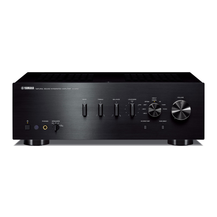
- Page 3 A-S701 ■ IMPEDANCE SELECTOR WARNING: Do not change the setting of the IMPEDANCE SELECTOR switch when the unit power is switched on, as doing so may damage the unit. IMPEDANCE SELECTOR ■ FRONT PANEL A-S701...
- Page 4 A-S701 ■ REAR PANELS A-S701 (U model) A-S701 (R model) A-S701 (A model)
- Page 5 A-S701 A-S701 (B, G models) A-S701 (L model)
- Page 6 A-S701 ■ REMOTE CONTROL PANEL ■ SPECIFICATIONS ■ Audio Section RAS14 Minimum RMS Output Power (Power Amp. Section) (20 Hz to 20 kHz) 8 ohms, 0.019 % THD ..........100 W + 100 W 6 ohms, 0.038 % THD ..........120 W + 120 W Dynamic Power Per Channel (IHF) 8 / 6 / 4 / 2 ohms ..........140 / 170 / 220 / 290 W...
- Page 7 A-S701 Channel Separation • DIMENSIONS CD, etc. (Input 5.1 k-ohms shorted) Top view 1 kHz ................. 65 dB or more 10 kHz ............... 50 dB or more ø 60 Tone Control Characteristics BASS Boost/Cut (20 Hz) ..............±10 dB Turnover frequency ...............400 Hz TREBLE Boost/Cut (20 kHz) ............... ±10 dB Turnover frequency ..............3.5 kHz Continuous Loudness Control Attenuation (1 kHz) ..............
- Page 8 A-S701 ■ INTERNAL VIEW Top view a MAIN (8) b MAIN (2) c FUNCTION (4) d MAIN (3) (R model) e DIGITAL f MAIN (6) g FUNCTION (1) h FUNCTION (2) i FUNCTION (3) j MAIN (5) k MAIN (1)
- Page 9 A-S701 ■ DISASSEMBLY PROCEDURES (Remove parts in the order as numbered.) Disconnect the power cable from the AC outlet. 1. Removal of Top Cover Remove 4 screws (1), 4 screws (2) and screw (3). (Fig. 1) b. Remove the top cover. (Fig. 1) 2.
- Page 10 A-S701 3. Removal of Sub-chassis Unit Remove 2 screws ( ⑧ ). (Fig. 2) b. Remove CB505, CB508, CB706 and CB853. (Fig. 2) Release 2 hooks and then remove the sub-chassis unit. (Fig. 2) 4. Removal of DIGITAL P.C.B. Remove 3 screws (9). (Fig. 3) b.
- Page 11 A-S701 When checking the P.C.B.s: • Put the rubber sheet and the cloth over this unit, Then place the sub-chassis unit on the cloth and check it. (Fig. 4) • Connect the ground point of the sub-chassis unit to the chassis with a ground lead or the like. (Fig. 4) •...
- Page 12 A-S701 ■ UPDATING FIRMWARE When the following parts are replaced, the firmware must be updated to the latest version. FUNCTION P.C.B. ● Confirmation of firmware version Before and after updating the firmware, check the firmware version by using the self-diagnostic function menu.
- Page 13 A-S701 ● Connection Use the optical cable (when OPTICAL jack is used) or Digital audio pin cable (when COAXIAL jack is used) to connect the CD, DVD or BD player and the unit. ● Operation Procedures Set this unit to the firmware update mode.
- Page 14 A-S701 After the firmware has been updated, all “INPUT” indicators light up. (Fig. 4) Update is completed Fig. 4 After checking that all “INPUT” indicators light up, press the “z” (power) switch to turn it off, then on again. Note: If the power indicator flashes at a 0.5-second interval or all “INPUT”...
- Page 15 A-S701 ■ SELF-DIAGNOSTIC FUNCTION This unit has self-diagnostic functions that provides the following functions. • Indication of firmware version • Indication of “AUTO POWER STANDBY” switch status • Indication and checking of protection information • Factory preset ● Starting Self-Diagnostic Function Press the “z”...
- Page 16 A-S701 ● Display provided when Self-Diagnostic Function started ・ Indication of firmware version ・ Indication of protection information Power indicator INPUT indicators ・ Indication of auto power standby status Fig. 3 ● Details of Indication • Indication of firmware version The firmware version of the microprocessor (IC502 of the FUNCTION P.C.B.) is indicated in the binary code (BCD) using...
- Page 17 A-S701 • Indication of protection information The protection information is indicated by the flashing pattern of the “z”(power) indicator. Power indicator flashing pattern : Lit Types of protection function / : Off Flashing 2 / PS protection / 500mS 500mS...
- Page 18 A-S701 Diode THM protection Cause: Abnormal temperature of diode (D111 of MAIN (1) P.C.B). Normal value: 0 to 0.346V (AD value: 0-18) Detection port: THM3 (FUNCTION (1) P.C.B. 97 pin of the microprocessor IC502) Detected at: THM3 (TH501 of FUNCTION (4) P.C.B., D111 of MAIN (1) P.C.B.) •...
- Page 19 A-S701 Example: To check the history for the 3rd most recent protection function, set the “SPEAKERS” knob to “OFF”, the “BASS” and “TREBLE” knobs to their top positions, the “LOUDNESS” knob to “FLAT”, and the “BALANCE” knob to “L”. (Fig. 8) Fig.
- Page 20 A-S701 AD value for diode THM (temperature) Turn the “TREBLE” knob to “+” and the “SPEAKERS” knob to “OFF”. (Fig. 11) The AD value for the diode THM (temperature) (TH501 on FUNCTION (4) P.C.B. and D111 on MAIN (1) P.C.B.) is indicated in binary code (BCD) using the “INPUT”...
- Page 21 A-S701 AD value for the “BALANCE” knob (Fig. 14) Turn the “TREBLE” knob to “+” and the “SPEAKERS” knob to “B”. The position of the “BALANCE” knob when the protection function was activated is indicated in binary code (BCD) using the “INPUT”...
- Page 22 A-S701 Indication of input source The input source when the protection function was activated is indicated. Turn the “TREBLE” knob to “+” and the “SPEAKERS” knob to “A+B”. ( Fig. 17) The input source selected when the protection function was activated is indicated using the “INPUT” indicators. (Fig. 17) If CD was the input source when the protection function was activated, the “CD”...
- Page 23 A-S701 ● Canceling Self-Diagnostic Function To keep setup information stored in the backup memory of the microprocessor: Set the “SPEAKERS” knob to the “OFF”, “B” or “A+B” position and press the “z” (power) key to turn off the power. Self-diagnostic function is canceled.
- Page 24 A-S701 ● Starting in the Protection Cancel mode CAUTION! Using this product with the protection function disabled may cause further damage to this unit. Use special care for this point when using this mode. If the protection function works and causes hindrance to trouble shoot, cancel the protection function as described below, and it will be possible to enter the self-diagnostic function mode.
- Page 25 A-S701 Notes: • Applying the power to this unit without correcting the abnormality can be dangerous and cause additional circuit damage. To avoid this, if protection function has been activated the number of times which is set beforehand, the power will not turn on even when the “z” (power) switch is pressed.
- Page 26 A-S701 ■ POWER AMPLIFIER ADJUSTMENT ● CONFIRMATION OF IDLING CURRENT 1. Right after power is turned on, confirm that the voltage across the terminals of R156-R159 (L ch) and R157-R158 (R ch) are between 0.1 mV and 10 mV. 2. If measured voltage exceeds 10 mV, open (cut off) R139 (L ch), R142 (R ch) and reconfirm the voltage.
- Page 27 A-S701 SCHEMATIC DIAGRAM MAIN (1) 6 m A 1 m A R 1 6 6 1 0 K Q 1 1 3 Q 1 4 0 R 1 4 8 1 m A R 1 6 7 6 0 V Q 1 1 9 1 P 4 .
- Page 28 A-S701 ■ IC DATA IC502: R5F3640ECNFA (FUNCTION P.C.B.) Single chip 16-bit microprocessor Port P0 Port P1 Port P2 Port P3 Port P4 Port P5 VCC2 ports Internal peripheral functions System clock generator UART or clock synchronous serial I/O Timer (16-bit)
- Page 29 A-S701 Function Name Port Name Detail of Function (P.C.B.) P9_6/ANEX1/SOUT4 HP_DET Headphone detection terminal P9_5/ANEX0/CLK4 TRIG CONTROL +12V control P9_4/DA1/TB4IN MPLED LED control for MAIN POWER ON display P9_3/DA0/TB3IN EXT_N_RST EXT IC reset signal P9_2/TB2IN/SOUT3 EXT_MOSI EXT IC serial data...
- Page 30 A-S701 Function Name Port Name Detail of Function (P.C.B.) P4_3/A19 Encoder phase detection input/output for Input selector P4_2/A18 Encoder phase detection input/output for Input selector P4_1/A17 CD_LED CD Direct LED control P4_0/A16 PD_LED Pure Direct LED control P3_7/A15 DIGITAL_PON Digital power supply 5V control signal of DIGITAL printed circuit boards...
- Page 31 A-S701 ■ PIN CONNECTION DIAGRAMS • ICs LC709004AMJ LM61CIZ BD3473KS2 BH6578FVM-TR HEF4013BP EL816 HEF4053BT 1: Anode 2: Cathode 3: Emitter 4: Collector NJM2068MD-TE2 NJM2388F05 NJM4580E PCM5101APWR PCM9211PTR NJM5532M-D 1. V 2. V 3. GND 4. ON/OFF CONTROL RP130Q331D-TR-F RP170H331 TC7WHU04FK...
- Page 32 A-S701 MEMO...
- Page 33 A-S701 ■ BLOCK DIAGRAM IC601 VOL IC NJM2068MD-TE2 EQ AMP EQ AMP IC402 YD953A0 PHONO REC OUT suppression REC OUT suppression OPERATION TUNER IC401 MAIN Volume • See page 56-57 → Zone2 LINE1 (+24dB 〜-95dB/0.5dBstep) SCHEMATIC DIAGRAM • See page 58-59 →...
- Page 34 A-S701 ■ WIRING DIAGRAMS • OVERALL ASSEMBLY DIGITAL P.C.B. UNUIT Fix the wire by style pin (Assemble this unit before attach to rear panel) not to touch with heatsink. Fix the wire by cable tie not to touch with heatsink.
- Page 35 A-S701 ■ PRINTED CIRCUIT BOARDS DIGITAL (Side A) DC OUT DIGITAL COAXIAL OPTICAL CB302 IC309 IC305 IC304 IC301 IC303 IGND OPERATION (8) (CB21) CB301 CB303 CB304 FUNCTION (2) (W404) FUNCTION (2) (W403) B, G models • Semiconductor Location FUNCTION (1) Ref no.
- Page 36 A-S701 FUNCTION (4) (Side A) to DIODE temperature FUNCTION (1) MAIN (1) (Side A) OPERATION (1) (CB109) (CB801) OPERATION (3) (W803) DIGITAL (CB301) MAIN (2) OPERATION (8) (CB14) (CB2) For Self-Diagnostic Function mode. W505 W503 W501A CB508 CB505 W502 CB517...
- Page 37 A-S701 FUNCTION (4) (Side B) FUNCTION (1) (Side B) No replacement part available. 1 100 • Semiconductor Location Ref no. Location Ref no. Location D501 IC502 D502 Q503 D506 Q505 D508 Q510 D509 Q506 D512 Q507 D513 D514 D515...
- Page 38 A-S701 FUNCTION (2) FUNCTION (3) (Side A) (Side A) LINE TUNER PHONO DIGITAL DIGITAL (CB303) (CB304) DAC_R AGND DAC_L AGND B, G models CDL-I CDL+I CDR-I CDR+I AGND PHOL PHOR AGND AGND MI_SEL PREMT FUNCTION (1) (CB510) FUNCTION (1) (CB502)
- Page 39 A-S701 FUNCTION (2) FUNCTION (3) (Side B) (Side B) • Semiconductor Location Ref no. Location IC401 IC402 IC407 IC409 IC601 IC602 IC603 Q411 Q412 Q413 Q414...
- Page 40 A-S701 OPERATION (1) (Side A) COAXIAL OPTICAL LINE 1 TUNER LINE 2 PHONO FUNCTION (1) (CB505) LINE 3 INPUT MPLED KEY1 MPSW L_DIN L_CLK L_CS L_RES KEY0 *MPLED CD DIRECT PURE DIRECT indicator indicator KEY1 MPSW FUNCTION (4) (W801) CD DIRECT PURE DIRECT •...
- Page 41 A-S701 OPERATION (1) (Side B) IC801 • Semiconductor Location Ref no. Location IC801...
- Page 42 A-S701 OPERATION (2) (Side A) VOLUME OPERATION (3) (Side A) FUNCTION (1) (CB508) FUNCTION (1) (W504) +5MTR AD_VOL VRUP VRDN LOUDNESS BASS TREBLE BALANCE...
- Page 43 A-S701 OPERATION (2) OPERATION (3) (Side B) (Side B) IC852 • Semiconductor Location Ref no. Location D851 D852 IC852...
- Page 44 A-S701 OPERATION (4) OPERATION (5) (Side A) (Side A) PHONES OPERATION (6) OPERATION (7) (W806B) (W805B) MPSW KEY1 *MPLED OPERATION (1) (CB808) HPL77 SPAKERS HP_DET MAIN (1) (W10) OPERATION (6) OPERATION (7) (Side A) (Side A) (Power) OPERATION (4) (W805A)
- Page 45 A-S701 OPERATION (4) OPERATION (5) (Side B) (Side B) OPERATION (6) OPERATION (7) (Side B) (Side B) • Semiconductor Location Ref no. Location D715 D716 Q803...
- Page 46 A-S701 OPERATION (8) (Side A) POWER TRANSFORMER POWER TRANSFORMER DIGITAL (W301) U, A, B, G, L models FUNCTION (1) (W503) R model • Semiconductor Location Ref no. Location...
- Page 47 A-S701 OPERATION (8) (Side B) R model U, A, B, G, L models • Semiconductor Location Ref no. Location Ref no. Location...
- Page 48 A-S701 MAIN (1) (Side A) MAIN (5) (Side A) FUNCTION (1) to HEATSINK R temperature (W405) PREOUT_L AGND PREOUT_R FUNCTION (1) B, G models (W505) AGND PREMT SWMT POW_MGT SPBRY SPARY PRIY FUNCTION (2) (W401) CB105 CB101 Q122C Q124C Q124A...
- Page 49 A-S701 MAIN (1) (Side B) MAIN (4) (Side B) • Semiconductor Location Ref no. Location D101 D102 D103 D104 D105 D106 D107 D108 D109 D110 D112 D113 D114 D117 D118 D119 D120 D121 IC103 Q101 Q102 Q103 Q104 MAIN (5)
- Page 50 A-S701 MAIN (2) (Side A) MAIN (3) (Side A) R model OPERATION (5) (CB706) HP_DET CB10 Gray Gray Purple POWER TRANSFORMER White Purple POWER TRANSFORMER CB13 CB14 MAIN (1) FUNCTION (1) (W502) (W104) MAIN (6) (Side A) • Semiconductor Location...
- Page 51 A-S701 MAIN (2) (Side B) MAIN (3) (Side B) R model MAIN (6) (Side B) • Semiconductor Location Ref no. Location Q1002...
- Page 52 A-S701 MEMO MEMO...
- Page 53 A-S701 ■ SCHEMATIC DIAGRAMS DIGITAL D e s t i n a t i o n P a r t L i s t + - - - - - - - - + - - - - - - - - - - - - - - - + - - - - - - - - - - - - - - - + - - - - - - - - - - - - - - - + - - - - - - - - - - - - - - - +...
- Page 54 A-S701 IC402: BD3473KS2 Silicon Monolithic Integrated Circuit) FUNCTION 1/2 Page 56 Page 53 to OPERATION (1)_CB801 to DIGITAL_CB301 Page 53 Page 53 to DIGITAL_CB303 to DIGITAL_CB304 F F C c o n n e c t o r 1 . 2 5 m m P i t c h F F C c o n n e c t o r 1 .
- Page 55 A-S701 FUNCTION 2/2 P H O N O _ C D F U N C ( 3 ) 7 0 m m J Y 6 0 1 6 0 1 - FUNCTION (3) J K 6 0 1 n o _ u s e...
- Page 56 A-S701 OPERATION 1/2 F U N C _ L E D O P E ( 1 ) OPERATION (1) + 5 S + 5 M 5 2 0 4 4 n o _ u s e U S B _ L E D...
- Page 57 A-S701 OPERATION 2/2 MAIN Transformer Destination Part List +--------+---------------+-----------------+------- ----------+-----------------+-----------------+ (Except RL Destination) LOCATION +--------+---------------+-----------------+------- ----------+-----------------+-----------------+ WJ36120 WF 08150 WF08150 WF08150 0.047/400 0.0 47/630 0.047/630 0.047/630 (Except RL Dest.) +--------+---------------+-----------------+------- ----------+-----------------+-----------------+ WB69630 WF 08150 WF08150 WF08150 0.1/400 0.0 47/630 0.047/630 0.047/630...
- Page 58 A-S701 MAIN 1/2 B l u e / 1 1 5 V O r a n g e / 1 1 5 V Page 59 1 1 0 - 1 2 0 V 2 2 0 - 2 3 0 V...
- Page 59 A-S701 D e s t i n a t i o n P a r t L i s t MAIN 2/2 + - - - - - - - - + - - - - - - - - - - - - - - - + - - - - - - - - - - - - - - - + - - - - - - - - - - - - - - - + - - - - - - - - - - - - - - - + - - - - - - - - - - - - - - - + - - - - - - - - - - - - - - - + - - - - - - - - - - - - - - - +...
- Page 60 A-S701 ■ REPLACEMENT PARTS LIST • ELECTRICAL COMPONENT PARTS WARNING ● Components having special characteristics are marked ⚠ and must be replaced with parts having specifications equal to those originally installed. ● The chip resistor is not supplied as a replacement part.
- Page 61 A-S701 P.C.B. DIGITAL Ref No. Part No. Description Remarks Markets ZN157200 P.C.B. DIGITAL URAL ZN157300 P.C.B. DIGITAL ZN157400 P.C.B. DIGITAL CB301 WA901400 14P SE CB302 WG939700 CN.USB 4P SE CB303 LB919040 CN.BS.PIN CB304 VB858500 CN.BS.PIN C301 US035100 C.CE.CHP 0.1uF 16V B...
- Page 62 A-S701 P.C.B. DIGITAL and P.C.B. FUNCTION Ref No. Part No. Description Remarks Markets C361 UR237100 C.EL 10uF URAL C361 UU237100 C.EL 10uF IC301 YD216A00 PCM9211PTR * IC303 YG390A00 PCM5102APWR IC304 X6143A00 NJM2388F05 5.0V IC305 YC288A00 RP130Q331D-TR-F IC306 YF016A00 RP170H331B-T1-FE IC307...
- Page 63 A-S701 P.C.B. FUNCTION Ref No. Part No. Description Remarks Markets C448-449 UR038330 C.EL 330uF * C450-451 WY401300 C.PP 0.022uF 100V C462-463 WE102900 C.PP 0.01uF 100V J C467 UR037470 C.EL 47uF C468 US035100 C.CE.CHP 0.1uF 16V B C469-470 UR238100 C.EL 100uF...
- Page 64 A-S701 P.C.B. FUNCTION and P.C.B. OPERATION Ref No. Part No. Description Remarks Markets D512-515 WW783900 DIODE 1SS355VM IC401 X3505A00 NJM2068MD-TE2 URAL IC401 X9127A00 NJM5532M-D IC402 YD953A00 BD3473KS2 IC407 X3505A00 NJM2068MD-TE2 URAL IC407 X9127A00 NJM5532M-D * IC409 YG322A00 HEF4053BT IC601 X3505A00...
- Page 65 A-S701 P.C.B. OPERATION Ref No. Part No. Description Remarks Markets UR038470 C.EL 470uF UU266220 C.EL 2.2uF UR266220 C.EL 2.2uF ZD520000 C.MYLAR 0.01uF 100V WE102900 C.PP 0.01uF 100V J WJ361200 C.POL.MTL 0.047uF 400V WF081500 C.PP 0.047uF 630V J RABGL UU266100 C.EL...
- Page 66 A-S701 P.C.B. OPERATION and P.C.B. MAIN Ref No. Part No. Description Remarks Markets IC801 YE686A00 LC709004AMJ-AH * IC852 YD292A00 BH6578FVM-TR * JK701 ZK754000 JACK.PHONE JY-6355-03-070GD PN851 WS488500 STYLE.PIN L=90 #18 WC435100 TR.DGT KRC104S-RTK Q2-3 WC529400 KTC3875S Y GR RTK WC529400...
- Page 67 A-S701 P.C.B. MAIN Ref No. Part No. Description Remarks Markets C31-32 UR059220 C.EL 2200uF URAL C31-32 UR059470 C.EL 4700uF C35-36 UR267100 C.EL 10uF URAL C35-36 UR067100 C.EL 10uF C37-38 UR048330 C.EL 330uF URAL C37-38 UR048470 C.EL 470uF C103-104 UR237100 C.EL...
- Page 68 A-S701 P.C.B. MAIN Ref No. Part No. Description Remarks Markets ⚠ WH487300 DIODE.BRG RS203M 2.0A 200V D18-19 WY165000 DIODE.ZENR UDZV30B D20-21 WY163700 DIODE.ZENR UDZV8.2B WY165000 DIODE.ZENR UDZV30B D101-106 WW783900 DIODE 1SS355VM ⚠ * D107-108 ZA384100 DIODE.ZENR TFZGTR5.6B 5.6V D109-110 ZA984400...
- Page 69 A-S701 P.C.B. MAIN Ref No. Part No. Description Remarks Markets R101-102 V8070900 R.MTL.FLM 100 Ω R103-104 V8072700 R.MTL.OXD 47K Ω 1W J R105 V8070100 R.MTL.FLM 2.2 Ω R106-107 V8072600 R.MTL.OXD 33K Ω R108-109 V8071100 R.MTL.FLM 220 Ω ⚠ R110-111 V8071400 R.MTL.FLM...
- Page 70 A-S701 Carbon Resistors Value 1/4W Type Part No. 1/6W Type Part No. Value 1/4W Type Part No. 1/6W Type Part No. 1.0 Ω 3100 3100 11 kΩ 7110 7110 HJ35 HF85 HF45 HF45 1.8 Ω 3180 12 kΩ 7120 7120...
- Page 71 A-S701 • OVERALL ASSEMBLY L model 2-1 (8) 3-4 (2) 100 100 200-1 B, G models B, G models Amp unit 4 (2) 4 (3) 4 (1) R model Sub-chassis unit B, G models 3-4 (3) Front panel unit...
- Page 72 A-S701 Ref No. Part No. Description Remarks Markets Ref No. Part No. Description Remarks Markets ZN149300 P.C.B. ASSEMBLY OPERATION VD069600 PW HEAD S-TIGHT SCREW 4x8-10 MFNI33 ZN149400 P.C.B. ASSEMBLY OPERATION WE774300 BIND HEAD B-TIGHT SCREW MFZN2W3 ZN149500 P.C.B. ASSEMBLY OPERATION...
- Page 73 A-S701 • FRONT PANEL UNIT and SUB-SHASSIS UNIT Ref No. Part No. Description Remarks Markets ZM209400 FRONT PANEL 41640 ZM209500 FRONT PANEL 2-1 (3) WP080600 LENS WP081200 SIDE PLATE WP081100 SIDE PLATE ZM601300 LENS SUPPORT ZM601200 LENS SUPPORT WK863700 LENS...
- Page 74 A-S701 • AMP UNIT Ref No. Part No. Description Remarks Markets ⚠ # 3-1-1 VP768600 PAIR TRANSISTOR 2SA1694/C4467 OPY Q121A,Q121C,Q123A,Q123C 3-1-5 VV849300 RADIATION SHEET 19x24 3-1-6 VP922500 DAMPER 2x10x170 3-1-7 VK173200 SCREW TRANSISTOR 3x15 SP MFC2 ⚠ # 3-2-1 VP768600...
- Page 75 A-S701 ■ REMOTE CONTROL SCHEMATIC DIAGRAM PANEL KEY NO. LAYOUT KEY CODE Key No Function Customer Code Data Code 7986 04FB 7986 55AA U1 GPM6P1001A 7986 609F 7986 01FE 7E81 2AD5 CD DIRECT 7A85 56A9 PURE DIRECT 7A85 DD22 VSS_TX...
- Page 76 A-S701 MEMO...
- Page 77 A-S701...
Need help?
Do you have a question about the A-S701 and is the answer not in the manual?
Questions and answers