Table of Contents
Advertisement
Quick Links
QQ
3 7 63 1515 0
SERVICE MANUAL
Ver.1.0 2005. 02
• HCD-GNX88 is the Amplifier,
CD player, tape deck and tuner
section in MHC-GNX88.
TE
L 13942296513
The following are measured at
DIN power output (rated)
Continuous RMS power output (reference)
Inputs
VIDEO/MD (AUDIO) IN (phono jacks):
TV (AUDIO) IN (phono jack):
MIC (phone jack):
Outputs
VIDEO OUT (phono jack):
PHONES (stereo mini jack):
FRONT SPEAKER:
SURROUND SPEAKER:
SUBWOOFER OUT:
www
.
Sony Corporation
9-879-461-01
Audio Group
2005B02-1
Published by Sony Engineering Corporation
© 2005.02
http://www.xiaoyu163.com
AC 127 V, 60 Hz
180 + 180 watts
(6 ohms at 1 kHz, DIN)
225 + 225 watts
(6 ohms at 1 kHz, 10% THD)
voltage 250/450 mV,
impedance 47 kiloohms
voltage 250 mV,
impedance 47 kiloohms
sensitivity 1 mV,
impedance 10 kiloohms
max. output level 1 Vp-p,
unbalanced, Sync negative,
load impedance 75 ohms
accepts headphones of 8 ohms or more
Use only the supplied speaker
• SS-GNX88
Use only the supplied speaker
• SS-RSX80
Use only the supplied subwoofer
• SS-WGV88
x
ao
u163
y
i
http://www.xiaoyu163.com
HCD-GNX88
2 9
8
Model Name Using Similar Mechanism
CD
CD Mechanism Type
Section
Base Unit Name
Optical Pick-up Name
TAPE
Model Name Using Similar Mechanism
Q Q
Section
Tape Transport Mechanism Type
3
6 7
1 3
1 5
SPECIFICATIONS
Disc player section
System
Laser
Laser Output
Frequency response
Wave length
Signal-to-noise ratio
Dynamic range
OPTICAL CD DIGITAL OUT
(Square optical connector jack, rear panel)
Wave length
Output Level
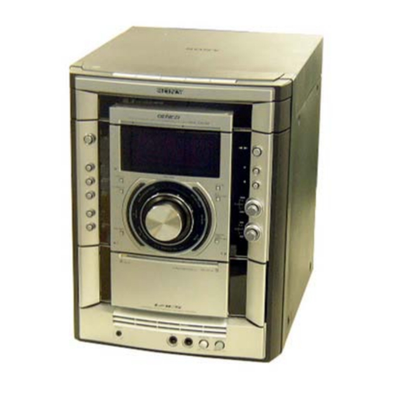
MiNi Hi-Fi COMPONENT SYSTEM
co
.
9 4
2 8
E Model
NEW
CDM74-F1BD84
BU-F1BD84
KSM-215DCP/C2NP
NEW
CMAT5Z2
0 5
8
2 9
9 4
2 8
Compact disc and digital audio system
Semiconductor laser
(λ=780 nm)
Emission duration: continuous
Max. 44.6 µW*
*This output is the value measured at a
distance of 200 mm from the objective lens
surface on the Optical Pick-up Block with 7
mm aperture.
2 Hz – 20 kHz (±0.5 dB)
780 – 790 nm
More than 90 dB
More than 90 dB
660 nm
–18 dBm
– Continued on next page –
m
9 9
9 9
Advertisement
Table of Contents

Related Manuals for Sony HCD-GNX88


Summary of Contents for Sony HCD-GNX88
- Page 1 HCD-GNX88 3 7 63 1515 0 SERVICE MANUAL E Model Ver.1.0 2005. 02 • HCD-GNX88 is the Amplifier, CD player, tape deck and tuner section in MHC-GNX88. Model Name Using Similar Mechanism CD Mechanism Type CDM74-F1BD84 Section Base Unit Name...
- Page 2 Recording system 4-track 2-channel stereo • Never reuse a disconnected chip component. Frequency response 50 – 13,000 Hz (±3 dB), using Sony • Notice that the minus side of a tantalum capacitor may be TYPE I tape damaged by heat.
-
Page 3: Table Of Contents
HCD-GNX88 3 7 63 1515 0 TABLE OF CONTENTS SERVICING NOTES ..........4 DIAGRAMS 7-1. Circuit Board Location ............ 26 GENERAL 7-2. Block Diagram – CDG Section – ........27 Location of Controls ............5 7-3. Block Diagram – Tape Section – ........28 7-4. -
Page 4: Servicing Notes
HCD-GNX88 SECTION 1 SERVICING NOTES 3 7 63 1515 0 • MODEL IDENTIFICATION NOTES ON HANDLING THE OPTICAL PICK-UP BLOCK – Back Panel – OR BASE UNIT PART No. The laser diode in the optical pick-up block may suffer electrostatic break-down because of the potential difference generated by the charged electrostatic load, etc. -
Page 5: General
HCD-GNX88 SECTION 2 GENERAL This section is extracted 3 7 63 1515 0 from instruction manual. LOCATING THE CONTROLS List of button location s and reference pages M a in unit ALPHABETICAL ORDER SYMBOLS M – R MASTER VOLUME 8 ?/1 (power) ra A –... - Page 6 HCD-GNX88 This section is extracted from instruction manual. 3 7 63 1515 0 Re m ot e c ont rol TAPE wd ALPHABETICAL ORDER TUNER/BAND 7 TUNER MEMORY wg A – E TUNING MODE 5 ALBUM + qf VOLUME +/– qg ALBUM –...
-
Page 7: Disassembly
HCD-GNX88 SECTION 3 DISASSEMBLY 3 7 63 1515 0 • This set can be disassembled in the order shown below. 3-1. DISASSEMBLY FLOW 3-2.SIDE PANEL, TOP CASE (Page 8) 3-3.LOADING PANEL ASSY (Page 8) 3-4.FRONT PANEL ASSY (Page 9) 3-7.PANEL BOARD,... -
Page 8: Side Panel, Top Case
HCD-GNX88 3 7 63 1515 0 Note: Follow the disassembly procedure in the numerical order given. 3-2. SIDE PANEL, TOP CASE qd CASE (TOP) 7 two screws (case 3 TP2) 8 two screws (3X12) (+BVTP 3X10) qa two screws... -
Page 9: Front Panel Assy
HCD-GNX88 3 7 63 1515 0 3-4. FRONT PANEL ASSY 7 connector (CN100) 9 CNP509 8 CNP508 4 screw (+BVTP 3X10) 3 screw (+BVTP 3X10) qa connector 6 front panel assy (CN1102) q; connector (CN503) 5 screw qs connector... -
Page 10: Tape Mechanism Deck, Mic Board
HCD-GNX88 3 7 63 1515 0 3-6. TAPE MECHANISM DECK, MIC BOARD 3 cover (TCM) 1 two screws 4 screw (+BVTP2.6 (3CR)) (+BVTP2.6 (3CR)) 2 two screws (+BVTP2.6 (3CR)) 5 tape mechanism deck 6 two screws (+BVTP2.6 (3CR)) 7 bracket (MIC) -
Page 11: Cd Mechanism Deck
HCD-GNX88 3 7 63 1515 0 3-8. CD MECHANISM DECK 1 CD mechanism deck 2 CNP505 3 CNP504 5 connector (CN560) 4 connector (CN701) L 13942296513 MAIN board 3-9. CDG BOARD 3 CDM cover 1 two screws (+BVTP 3X10) -
Page 12: Back Panel
HCD-GNX88 3 7 63 1515 0 3-10. BACK PANEL 5 back panel 2 connector 4 four screws (CN1204) (+BVTP 3X10) 1 connector (CN1200) 6 connector (CN580) 3 four screws (+BVTP 3X10) L 13942296513 3-11. PRIMARY BOARD 1 connector (CN101) -
Page 13: Power Amp Pc Board Assy, Main Board
HCD-GNX88 3 7 63 1515 0 3-12. POWER AMP PC BOARD ASSY, MAIN BOARD 4 two screws 5 screw (+BVTP 3X6) (+BVTP 3X6) 7 power amp pc board assy 3 screw (+BVTP 3X6) 6 screw 1 connector 8 connector... -
Page 14: Power Transformer (T1200)
HCD-GNX88 3 7 63 1515 0 3-14. POWER TRANSFORMER (T1200) TRANS board 5 power transfomer (T1200) 1 connector 4 two screws (CN1213) 2 connector (CN1212) 3 two screws L 13942296513 3-15. DRIVER BOARD, SW BOARD 1 two screws (+BTTP (M2.6)) -
Page 15: Bd84 Board
HCD-GNX88 3 7 63 1515 0 3-16. BD84 BOARD 1 floating screw (+PTPWH M2.6) 6 two insulators 2 h older (213) ASSY qh optical pick-up (KSM-215DCP/C2NP) 5 two coil springs (insulator) 0 two insulators 3 screw 9 two coil springs (BVTT M2.6) -
Page 16: Motor (Tb) Board
HCD-GNX88 3 7 63 1515 0 3-18. MOTOR (TB) BOARD 2 stopper 1 stopper 7 t able motor assy (M741) 3 wire (flat type) 5 core (CN742) 8 MOTOR (TB) board 6 Remove the two solderings of motor. 5 two screws L 13942296513 (+BTTP (M2.6)) -
Page 17: Test Mode
HCD-GNX88 SECTION 4 TEST MODE 3 7 63 1515 0 [GC TEST MODE] [MC TEST MODE] • This mode is used to check the fluorescent indicator tube, • This mode is used to check operations of the respective sections LEDs, keys, VOLUME jog, OPERATION DIAL jog, AMS of Amplifier, Tuner, and Tape. - Page 18 HCD-GNX88 3 7 63 1515 0 [VACS ON/OFF] [AGING MODE] • This mode is used to switch ON and OFF the VACS (Variable This mode can be used for operation check of CD section. Attenuation Control System). • If an error occurs, the aging operation would stops and the status is displayed.
- Page 19 HCD-GNX88 3 7 63 1515 0 • Display when an error occurred (CD Error Code Mode) 3) Display of no disc errors Procedure: Display 1. Press x button, [ENTER] button and [DISC 1] button simultaneously to enter the error code display mode.
- Page 20 HCD-GNX88 3 7 63 1515 0 [CD SHIP MODE (WITHOUT MEMORY CLEAR)] [CD TRAY LOCK MODE] • This mode moves the optical pick-up to the position durable • This mode let you lock the disc trays. When this mode is to vibration.
-
Page 21: Mechanical Adjustments
HCD-GNX88 SECTION 5 SECTION 6 3 7 63 1515 0 MECHANICAL ADJUSTMENTS ELECTRICAL ADJUSTMENTS Precaution DECK SECTION 0 dB=0.775 V 1. Clean the following parts with a denatured alcohol-moistened swab: 1. Demagnetize the record/playback head with a head record/playback heads pinch rollers demagnetizer. -
Page 22: Cd Section
HCD-GNX88 3 7 63 1515 0 2. Turn the adjustment screw and check output peaks. If the peaks CD SECTION do not match for L-CH and R-CH, turn the adjustment screw so that outputs match within 1dB of peak. -
Page 23: Http://Www.xiaoyu163.Com
HCD-GNX88 3 7 63 1515 0 RFAC Level Check E-F Balance Check Connection: Connection: oscilloscope oscilloscope BD84 board BD84 board TP124 (RFAC) TPO103 (TE1) TP117 (VC) – TP117 (VC) – Procedure: Procedure: 1. Connect an oscilloscope to test point TP124 (RFAC) and TP 1. - Page 24 HCD-GNX88 3 7 63 1515 0 Checking Location: – BD84 BOARD (SIDE B) – TP117 (VC) JPO103 (TE1) IC101 JPO102 (FE1) L 13942296513 TP124 (RFAC) u163 http://www.xiaoyu163.com...
-
Page 25: Diagrams
HCD-GNX88 SECTION 7 3 7 63 1515 0 DIAGRAMS Note on Printed Wiring Boards: For schematic diagrams. Note: Note: • X : parts extracted from the component side. • All capacitors are in µF unless otherwise noted. (p: pF) •... -
Page 26: Circuit Board Location
HCD-GNX88 3 7 63 1515 0 7-1. CIRCUIT BOARD LOCATION CDG board PRIMARY board CD-SW board TUNER PACK SWITCHING POWER TRANS board SURROUND board L 13942296513 PA board SENSOR board SW board BD84 board MOTOR (TB) board MOTOR (LD) board... -
Page 27: Block Diagram - Cdg Section
HCD-GNX88 3 7 6 3 1 5 1 5 0 7-2. BLOCK DIAGRAM – CDG SECTION – MAIN CD-L AOUT1 SECTION (Page 29) AOUT2 R-CH OPTICAL PICK-UP BLOCK IC101 CD MUTE CD MUTE DRIVE IC210 (KSM-215DCP/C2NP) Q250,251 RF AMP... -
Page 28: Block Diagram - Tape Section
HCD-GNX88 3 7 6 3 1 5 1 5 0 7-3. BLOCK DIAGRAM – TAPE SECTION – DECK-A AIN1 L – CH MAIN EQ OUT1 PB OUT1 TC-PB-L TAI1 SECTION HEAD (Page 29) R – CH R-CH CN510 BIN1... -
Page 29: Block Diagram - Main Section
HCD-GNX88 3 7 6 3 1 5 1 5 0 7-4. BLOCK DIAGRAM – MAIN SECTION – J1100(1/3) MIC 1 RV1100 MIC LEVEL J1101(1/3) MIC AMP MIC OUT REC-OUT-L MIC AMP TAPE MIC 2 IC1100(1/2) IC1100 (2/2) SECTION (Page 28) -
Page 30: Block Diagram - Amp Section
HCD-GNX88 3 7 6 3 1 5 1 5 0 7-5. BLOCK DIAGRAM – AMP SECTION – MAIN DBFB F/B SECTION J1103 (Page 29) PHONES IC600 POWER AMP D624 TM600 FRONT SPEAKER RY646 PROTECT SWITCH OVER LOAD TM601 Q666... -
Page 31: Block Diagram - Display Section
HCD-GNX88 3 7 6 3 1 5 1 5 0 7-6. BLOCK DIAGRAM – DISPLAY SECTION – LED+9V KEY2 S1149-1160 83 XIN S910,911,918,920,924 X901 KEY0 S901 – 904, 912,915,917 4MHz 82 XOUT Q905 Q907 Q906 P1 – 36 SELECTOR... -
Page 32: Printed Wiring Board - Bd84 Board
HCD-GNX88 3 7 6 3 1 5 1 5 0 7-7. PRINTED WIRING BOARD – BD84 BOARD – • See page 26 for Circuit Boards Location. : Uses unleaded solder. BD84 BOARD (SIDE B) BD84 BOARD (SIDE A) M101... -
Page 33: Schematic Diagram - Bd84 Board
HCD-GNX88 3 7 6 3 1 5 1 5 0 7-8. SCHEMATIC DIAGRAM – BD84 BOARD – • See page 52, 53 for IC Block Diagrams. • See page 52 for Waveforms. • See page 52 for IC Pin Function Description. -
Page 34: Printed Wiring Board - Cd Mechanism Board
HCD-GNX88 3 7 6 3 1 5 1 5 0 7-9. PRINTED WIRING BOARD – CD MECHANISM BOARD – • See page 26 for Circuit Boards Location. : Uses unleaded solder. 1 3 9 4 2 2 9 6 5 1 3... -
Page 35: Schematic Diagram - Cd Mechanism Board
HCD-GNX88 3 7 6 3 1 5 1 5 0 • See page 52 for IC Block Diagrams. 7-10. SCHEMATIC DIAGRAM – CD MECHANISM BOARD – 1 3 9 4 2 2 9 6 5 1 3 w w w... -
Page 36: Printed Wiring Boards - Main Board
HCD-GNX88 3 7 6 3 1 5 1 5 0 7-11. PRINTED WIRING BOARD – MAIN BOARD – • See page 26 for Circuit Boards Location. : Uses unleaded solder. BD84 BOARD DRIVER TUNER PACK (Page 32) PRIMARY (FOR CHECK) -
Page 37: Schematic Diagram - Main Board (1/3)
HCD-GNX88 3 7 6 3 1 5 1 5 0 7-12. SCHEMATIC DIAGRAM – MAIN BOARD (1/3) – • See page 52 for Waveforms. • See page 57 for IC Pin Function Description. 1 3 9 4 2 2 9 6 5 1 3... -
Page 38: Schematic Diagram - Main Board (2/3)
HCD-GNX88 3 7 6 3 1 5 1 5 0 7-13. SCHEMATIC DIAGRAM – MAIN BOARD (2/3) – 1 3 9 4 2 2 9 6 5 1 3 w w w u 1 6 3 HCD-GNX88 http://www.xiaoyu163.com... -
Page 39: Schematic Diagram - Main Board (3/3)
HCD-GNX88 3 7 6 3 1 5 1 5 0 7-14. SCHEMATIC DIAGRAM – MAIN BOARD (3/3)– • See page 52 for Waveforms. 1 3 9 4 2 2 9 6 5 1 3 w w w u 1 6 3 HCD-GNX88 http://www.xiaoyu163.com... -
Page 40: Printed Wiring Boards - Panel Board
HCD-GNX88 3 7 6 3 1 5 1 5 0 7-15. PRINTED WIRING BOARD – PANEL BOARD – • See page 26 for Circuit Boards Location. : Uses unleaded solder. PANEL BOARD (NOT USE ) • Semiconductor Location DISPLAY CD SYNC Ref. -
Page 41: Schematic Diagram - Panel Board
HCD-GNX88 3 7 6 3 1 5 1 5 0 7-16. SCHEMATIC DIAGRAM – PANEL BOARD – • See page 52 for IC Block Diagrams. • See page 52 for Waveforms. • See page 59 for IC Pin Function Description. -
Page 42: Printed Wiring Board - Cd-Sw, Jog, Mic Boards
HCD-GNX88 3 7 6 3 1 5 1 5 0 7-17. PRINTED WIRING BOARD – CD-SW, JOG, MIC BOARDS – • See page 26 for Circuit Boards Location. : Uses unleaded solder. CD-SW BOARD PANEL BOARD (Page 40) Z OPEN/CLOSE... -
Page 43: Schematic Diagram - Cd-Sw, Jog, Mic Board
HCD-GNX88 3 7 6 3 1 5 1 5 0 7-18. SCHEMATIC DIAGRAM – CD-SW, JOG, MIC BOARDS BOARD – 1 3 9 4 2 2 9 6 5 1 3 w w w u 1 6 3 HCD-GNX88... -
Page 44: Printed Wiring Board - Pa Board
HCD-GNX88 3 7 6 3 1 5 1 5 0 7-19. PRINTED WIRING BOARD – PA BOARD – • See page 26 for Circuit Boards Location. : Uses unleaded solder. MAIN MAIN BOARD BOARD BOARD (Page 36) (Page 42) -
Page 45: Schematic Diagram - Pa Board
HCD-GNX88 3 7 6 3 1 5 1 5 0 7-20. SCHEMATIC DIAGRAM – PA BOARD – 1 3 9 4 2 2 9 6 5 1 3 w w w u 1 6 3 HCD-GNX88 http://www.xiaoyu163.com... -
Page 46: Printed Wiring Board - Surround Board
HCD-GNX88 3 7 6 3 1 5 1 5 0 7-21. PRINTED WIRING BOARD – SURROUND BOARD – • See page 26 for Circuit Boards Location. : Uses unleaded solder. SURROUND BOARD BOARD (Page 44) 1 3 9 4 2 2 9 6 5 1 3... -
Page 47: Schematic Diagram -Surround Board
HCD-GNX88 3 7 6 3 1 5 1 5 0 7-22. SCHEMATIC DIAGRAM –SURROUND BOARD – 1 3 9 4 2 2 9 6 5 1 3 w w w u 1 6 3 HCD-GNX88 http://www.xiaoyu163.com... -
Page 48: Printed Wiring Board - Cdg Boards
HCD-GNX88 3 7 6 3 1 5 1 5 0 7-23. PRINTED WIRING BOARD – CDG BOARD – • See page 26 for Circuit Boards Location. : Uses unleaded solder. MAIN BOARD (Page 36) BOARD MAIN BOARD (Page 36) -
Page 49: Schematic Diagram - Cdg Boards
HCD-GNX88 3 7 6 3 1 5 1 5 0 • See page 52 for IC Block Diagrams. • See page 52 for Waveforms. 7-24. SCHEMATIC DIAGRAM – CDG BOARD – 1 3 9 4 2 2 9 6 5 1 3... -
Page 50: Printed Wiring Board - Trans, Primary Boards
HCD-GNX88 3 7 6 3 1 5 1 5 0 7-25. PRINTED WIRING BOARD – TRANS, PRIMARY BOARDS – • See page 26 for Circuit Boards Location. : Uses unleaded solder. T1200 TRANS BOARD POWER TRANSFORMER BOARD (Page 44) -
Page 51: Schematic Diagram - Trans, Primary Boards
HCD-GNX88 3 7 6 3 1 5 1 5 0 7-26. SCHEMATIC DIAGRAM – TRANS, PRIMARY BOARD – 1 3 9 4 2 2 9 6 5 1 3 w w w u 1 6 3 HCD-GNX88 http://www.xiaoyu163.com... - Page 52 HCD-GNX88 3 7 6 3 1 5 1 5 0 • IC Block Diagram • WAVEFORMS – BD84 BOARD – – MAIN BOARD – – PANEL BOARD – – DRIVER Board – – PANEL Board – IC701, 712 BA6956AN...
- Page 53 HCD-GNX88 3 7 63 1515 0 – BD84 Board – IC301 TC94A34FG-002 LRCKIA CS/RAS/ADO2 AD15/CAS/PD12 BCKIA SDO3/OE SDI0 PO11/BUCK/AD14 LRCKO PO10/CCE/AD13 BCKO PO9/AD12 SDO0 PO08/AD11 L 13942296513 VDDM VDDT SRMSTB MIACK MICK VDDT AD10 MIDIO MILP Switch MICS STANBY...
-
Page 54: Ic Pin Function Description
HCD-GNX88 3 7 63 1515 0 7-27. IC Pin Function Descriptions • IC101 CXD3059AR (RF AMP) (BD84 BOARD) Pin No. Pin Name Description MIRR Not used (Open) DFCT Not used (Open) Not used (Open) — Ground LOCK Not used (Open) - Page 55 HCD-GNX88 3 7 63 1515 0 Pin No. Pin Name Description AVSS3 — Ground CLTV Multiplier VCO1 control voltage input FILO Master PLL (slave = digital PLL) filter output FILI Master PLL filter input Master PLL charge pump output AVDD5 —...
- Page 56 HCD-GNX88 3 7 63 1515 0 Pin No. Pin Name Description EXCK SBSO readout clock input XRST System reset input from M30622MEP SYSM Mute input (Connected to ground) DATA Serial data input from M30622MEP — Ground XLAT Latch input from M30622MEP...
- Page 57 HCD-GNX88 3 7 63 1515 0 • IC401 M30622MEP-A02FPUO SYSTEM CONTROL (MAIN Board) Pin No. Pin Name Description XRST Reset signal output to CXD3053AR CD-DATA Serial data output to CXD3053AR XLAT Serial data latch signal output to CXD3053AR SIRCS...
- Page 58 HCD-GNX88 3 7 63 1515 0 Pin No. Pin Name Description SW LED2 LED drive signal output B-PLAY Deck B playback detection signal input THERMAL VACS Thermal VACS detection input A-TRIG Deck A side trigger plunger drive signal output...
- Page 59 HCD-GNX88 3 7 63 1515 0 • IC902 MB90M407PF-G-144-BNDE1 DISPLAY CONTROL (PANEL Board) Pin No. Pin Name Description 1 to 8 G8 to G1 FLD grid signal output 9, 10 P1,P2 FLD segment signal output VSS-IO — Ground 12 to 22...
-
Page 60: Exploded Views
HCD-GNX88 SECTION 8 EXPLODED VIEWS 3 7 63 1515 0 NOTE: • The mechanical parts with no reference number • -XX, -X mean standardized parts, so they may The components identified by mark 0 or in the exploded views are not supplied. -
Page 61: Front Panel Section
HCD-GNX88 3 7 63 1515 0 8-2. FRONT PANEL SECTION not supplied FL901 not supplied not supplied not supplied L 13942296513 not supplied supplied not supplied 52 53 Ref. No. Part No. Description Remarks Ref. No. Part No. Description... -
Page 62: Chassis Section
HCD-GNX88 3 7 63 1515 0 8-3. CHASSIS SECTION not supplied not supplied not supplied F1281 F1271 F1241 F1261 F1251 L 13942296513 T1200 not supplied The components identified by mark 0 or dotted line with mark 0 are critical for safety. -
Page 63: Cd Mechanism Deck Section-1 (Cdm74-F1Bd84)
HCD-GNX88 3 7 63 1515 0 8-4. CD MECHANISM DECK SECTION-1 (CDM74-F1BD84) M741 L 13942296513 CD mechanism deck section-2 Ref. No. Part No. Description Remarks Ref. No. Part No. Description Remarks 4-218-253-32 SCREW (M2.6), +BTTP 1-687-132-12 SENSOR BOARD 1-776-182-11 WIRE (FLAT TYPE) (5 CORE) -
Page 64: Cd Mechanism Deck Section-2 (Cdm74-F1Bd84)
HCD-GNX88 3 7 63 1515 0 8-5. CD MECHANISM DECK SECTION-2 (CDM74-F1BD84) RE701 M751 L 13942296513 not supplied The components identified by mark 0 or dotted line with mark 0 are critical for safety. Replace only with part number specified. -
Page 65: Electrical Parts List
HCD-GNX88 SECTION 9 BD84 ELECTRICAL PARTS LIST 3 7 63 1515 0 NOTE: • Due to standardization, replacements in the • RESISTORS The components identified by mark 0 parts list may be different from the parts All resistors are in ohms. - Page 66 HCD-GNX88 BD84 3 7 63 1515 0 Ref. No. Part No. Description Remarks Ref. No. Part No. Description Remarks < IC > R403 1-216-809-11 METAL CHIP 1/10W R404 1-216-809-11 METAL CHIP 1/10W IC101 8-752-425-12 IC CXD3059AR R405 1-216-809-11 METAL CHIP...
- Page 67 HCD-GNX88 CD-SW DRIVER 3 7 63 1515 0 Ref. No. Part No. Description Remarks Ref. No. Part No. Description Remarks < DIODE > R1029 1-216-809-11 METAL CHIP 1/10W R1030 1-216-837-11 METAL CHIP 1/10W D1003 8-719-988-61 DIODE 1SS355TE-17 R1031 1-218-285-11 METAL CHIP...
- Page 68 HCD-GNX88 DRIVER MAIN 3 7 63 1515 0 Ref. No. Part No. Description Remarks Ref. No. Ref. No. Part No. Part No. Description Description Remarks Remarks < RESISTOR > < SWITCH > R701 1-249-413-11 CARBON 1/4W S1161 1-479-203-11 ROTARY ENCODER (OPERATION DIAL)
- Page 69 HCD-GNX88 MAIN 3 7 63 1515 0 Ref. No. Part No. Description Remarks Ref. No. Part No. Description Remarks C223 1-104-658-91 ELECT 100uF C419 1-162-960-11 CERAMIC CHIP 220PF C230 1-136-497-81 FILM 0.1uF C429 1-162-923-11 CERAMIC CHIP 47PF C430 1-162-923-11 CERAMIC CHIP...
- Page 70 HCD-GNX88 MAIN 3 7 63 1515 0 Ref. No. Part No. Description Remarks Ref. No. Part No. Description Remarks * CN508 1-569-934-11 SOCKET, CONNECTOR 17P JR002 1-216-296-11 SHORT CHIP * CN509 1-569-930-11 SOCKET, CONNECTOR 13P JR003 1-216-864-11 SHORT CHIP...
- Page 71 HCD-GNX88 MAIN 3 7 63 1515 0 Ref. No. Part No. Description Remarks Ref. No. Part No. Description Remarks Q372 8-729-802-80 TRANSISTOR 2SC3661 R183 1-216-841-11 METAL CHIP 1/10W Q373 8-729-802-80 TRANSISTOR 2SC3661 R184 1-216-821-11 METAL CHIP 1/10W Q374 8-729-802-80 TRANSISTOR 2SC3661...
- Page 72 HCD-GNX88 MAIN 3 7 63 1515 0 Ref. No. Part No. Description Remarks Ref. No. Part No. Description Remarks R312 1-216-809-11 METAL CHIP 1/10W R406 1-216-809-11 METAL CHIP 1/10W R319 1-216-825-11 METAL CHIP 2.2K 1/10W R407 1-216-809-11 METAL CHIP...
- Page 73 HCD-GNX88 MAIN 3 7 63 1515 0 Ref. No. Part No. Description Remarks Ref. No. Part No. Description Remarks R491 1-216-809-11 METAL CHIP 1/10W A-1089-466-A MIC BOARD, COMPLETE R492 1-216-829-11 METAL CHIP 4.7K 1/10W ******************* R493 1-216-829-11 METAL CHIP 4.7K...
- Page 74 HCD-GNX88 MOTOR (LD) MOTOR (TB) 3 7 63 1515 0 Ref. No. Part No. Description Remarks Ref. No. Part No. Description Remarks IC1101 8-759-496-41 IC M65850FP-E1 1-687-134-12 MOTOR (TB) BOARD **************** < JACK > < CONNECTOR > J1100 1-817-630-11 JACK (LARGE TYPE) (MIC 1)
- Page 75 HCD-GNX88 3 7 63 1515 0 Ref. No. Part No. Description Remarks Ref. No. Part No. Description Remarks < DIODE > R610 1-216-843-11 METAL CHIP 1/10W R611 1-216-839-11 METAL CHIP 1/10W D609 8-719-988-61 DIODE 1SS355TE-17 0 R612 1-245-605-51 FUSIBLE...
- Page 76 HCD-GNX88 PANEL 3 7 63 1515 0 Ref. No. Part No. Description Remarks Ref. No. Part No. Description Remarks R669 1-216-821-11 METAL CHIP 1/10W C923 1-162-970-11 CERAMIC CHIP 0.01uF R670 1-216-839-11 METAL CHIP 1/10W C924 1-162-927-11 CERAMIC CHIP 100PF...
- Page 77 HCD-GNX88 PANEL 3 7 63 1515 0 Ref. No. Part No. Description Remarks Ref. No. Part No. Description Remarks D902 8-719-038-54 DIODE SEL6414E-LC05 (^/1) Q907 8-729-027-43 TRANSISTOR DTC114EKA-T146 D903 6-500-522-21 DIODE 10EDB40-TB3 Q908 8-729-027-43 TRANSISTOR DTC114EKA-T146 D904 6-500-522-21 DIODE 10EDB40-TB3...
- Page 78 HCD-GNX88 PANEL PRIMARY 3 7 63 1515 0 Ref. No. Part No. Description Remarks Ref. No. Part No. Description Remarks R961 1-216-823-11 METAL CHIP 1.5K 1/10W R1179 1-216-824-11 METAL CHIP 1.8K 1/10W R962 1-216-823-11 METAL CHIP 1.5K 1/10W R1180...
- Page 79 HCD-GNX88 PRIMARY SENSOR SURROUND 3 7 63 1515 0 Ref. No. Part No. Description Remarks Ref. No. Part No. Description Remarks < DIODE > < CONNECTOR > D1200 8-719-988-61 DIODE 1SS355TE-17 CN700 1-784-031-41 CONNECTOR, BOARD TO BOARD 8P CN800 1-778-227-41 CONNECTOR, BOARD TO BOARD 6P <...
- Page 80 HCD-GNX88 SURROUND TRANS 3 7 63 1515 0 Ref. No. Part No. Description Remarks Ref. No. Part No. Description Remarks R891 1-216-845-11 METAL CHIP 100K 1/10W MISCELLANEOUS ************* R892 1-245-711-31 CARBON 1/2W 1-693-671-11 TUNER (TM-10E) < RELAY > 1-468-737-21 POWER, SWITCHING...
- Page 81 HCD-GNX88 3 7 63 1515 0 MEMO L 13942296513 u163 http://www.xiaoyu163.com...
- Page 82 HCD-GNX88 3 7 63 1515 0 REVISION HISTORY Clicking the version allows you to jump to the revised page. Also, clicking the version at the upper right on the revised page allows you to jump to the next revised page.
Need help?
Do you have a question about the HCD-GNX88 and is the answer not in the manual?
Questions and answers