Table of Contents
Advertisement
SERVICE MANUAL
Ver. 1.2 2007.10
• HCD-GN1100D is the Amplifier,
DVD player, tape deck and tuner
section in MHC-GN1100D.
Amplifier section
The following are measured at AC 120, 127, 220,
240V 50/60 Hz
Power output (rated): 130 W + 130 W
RMS output power (reference)
Front speaker:
Center speaker:
Surround speaker:
Subwoofer:
Inputs
VIDEO INPUT:
TV/SAT AUDIO IN L/R:
MIC 1 or 2:
AUDIO OUT:
VIDEO OUT:
Sony Corporation
9-887-683-03
Personal Audio Division
2007J02-1
Published by Sony Techno Create Corporation
© 2007.10
HCD-GN1100D
DVD
Section
TAPE
Section
SPECIFICATIONS
(6 Ω , 1 kHz, 1% THD)
215 W + 215 W
(per channel at 6 Ω , 1 kHz, 10%
THD)
85 W
(per channel at 6 Ω , 1 kHz, 10%
THD)
90 W + 90 W
(per channel at 6 Ω , 1 kHz, 10%
THD)
210 W (per channel at 8 Ω , at 100 Hz,
10% THD)
VIDEO: 1 Vp-p, 75 ohms
AUDIO L/R: Voltage 250 mV,
impedance 47 kilohms
Voltage 250 mV/450 mV, impedance
47 kilohms
Sensitivity 1 mV, impedance
10 kilohms
Outputs
Voltage 250 mV, impedance 1 kilohm
Max. output level 1 Vp-p, unbalanced,
Sync. negative load impedance
75 ohms
Model Name Using Similar Mechanism
DVD Mechanism Type
Optical Pick-up Name
Model Name Using Similar Mechanism
Tape Transport Mechanism Type
COMPONENT VIDEO OUT:
S VIDEO OUT:
PHONES:
Disc player section
System
Laser
Frequency response
Video color system format
MINI HI-FI COMPONENT SYSTEM
E Model
HCD-GN1000D
CDM74HF-DVBU101
KHM-313CAB/C2NP
HCD-GN1000D
CWN42RR603
Y: 1 Vp-p, 75 ohms
PB/CB: 0.7 Vp-p, 75 ohms
PR/CR: 0.7 Vp-p, 75 ohms
Y: 1 Vp-p, unbalanced, Sync. negative
C: 0.286 Vp-p, load impedance
75 ohms
accepts headphones of 8 ohms or more
Compact disc and digital audio and
video system
Semiconductor laser (DVD: λ =650 nm,
CD: λ = 790 nm)
Emission duration: continuous
DVD (PCM 48 kHz): 2 Hz – 22 kHz
(±1 dB)
CD: 2 Hz – 20 kHz (±0.5 dB)
Latin American models: NTSC
Russian models: PAL
Other models: NTSC and PAL
– Continued on next page –
Advertisement
Table of Contents

Related Manuals for Sony HCD-GN1100D


Summary of Contents for Sony HCD-GN1100D
- Page 1 HCD-GN1100D SERVICE MANUAL E Model Ver. 1.2 2007.10 • HCD-GN1100D is the Amplifier, DVD player, tape deck and tuner section in MHC-GN1100D. Model Name Using Similar Mechanism HCD-GN1000D DVD Mechanism Type CDM74HF-DVBU101 Section Optical Pick-up Name KHM-313CAB/C2NP Model Name Using Similar Mechanism...
- Page 2 [VER.X.XX] (X is a number) may 450 kHz appear on the TV screen. Although this is not a General malfunction and for Sony service use only, Power requirements normal system operation will not be possible. Saudi Arabian model: 120 – 127 V, Turn off the system, and then turn on the system 220 V or 230 –...
-
Page 3: Table Of Contents
HCD-GN1100D TABLE OF CONTENTS DIAGRAMS ............25 SERVICING NOTES ..........4 7-1. Block Diagram – RF Section – ........27 7-2. Block Diagram – Video Section – ........28 GENERAL ..............5 7-3. Block Diagram – Tape/Tuner Section – ......29 7-4. -
Page 4: Servicing Notes
E3 : 240V AC Area in E model LIST ARE CRITICAL TO SAFE OPERATION. REPLACE THESE E12 : 220V-240V AC Area in E model COMPONENTS WITH SONY PARTS WHOSE PART NUMBERS E15 : Iran model APPEAR AS SHOWN IN THIS MANUAL OR IN SUPPLEMENTS EA : Saudi Arabia model PUBLISHED BY SONY. -
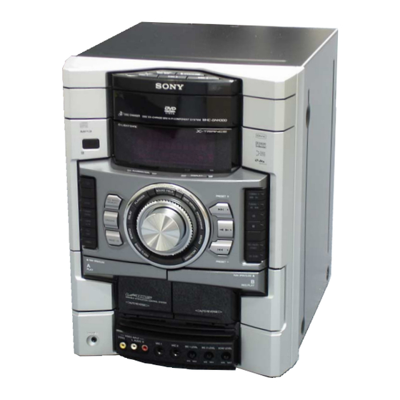
Page 5: General
HCD-GN1100D SECTION 2 GENERAL This section is extracted from instruction manual. LOCATING THE CONTROLS Q ECHO LEVEL 1 EQ BAND/MEMORY Turn to adjust the microphone echo Press to select a frequency band effect. when adjusting the graphic equalizer. R MIC 1/2 (jack) B FLANGER Connect the microphones. - Page 6 HCD-GN1100D REMOTE CONTROL Setting the clock 1 THEATRE SYNC TUNING +/– Press "/1 to turn on the system. Press to operate the THEATRE Press to tune in a radio station. SYNC function. Press TIMER MENU. SLOW /SLOW B TV "/1 (on/standby) The hour indication flashes in the Press to watch frame by frame.
-
Page 7: Disassembly
HCD-GN1100D SECTION 3 DISASSEMBLY Note: • This set can be disassembled in the order shown below. 3-1. DISASSEMBLY FLOW 3-2. CASE (Page 8) 3-3. LOADING PANEL (Page 8) 3-4. TUNER PACK (Page 9) 3-5. DVD MECHANISM DECK (Page 9) 3-10. KARAOKE BOARD,... -
Page 8: Case
HCD-GN1100D 3-2. CASE 7 three screws 9 case (+BVTP 3 × 10) 6 two screws 4 screw (+BVTP 3 × 10) (case 3 TP2) (3 × 12) 2 screw (case 3 TP2) (3 × 12) 5 two screws (+BVTP 3 × 10) -
Page 9: Tuner Pack
HCD-GN1100D 3-4. TUNER PACK 3 tuner pack 2 wire (flat type) (CN1) 1 two screws (+BVTP 3 × 8) 3-5. DVD MECHANISM DECK 6 DVD mechanism deck qd connector 9 connector (CN802) (CN505) 8 wire (flat type) 3 three screws (CN521) (+BVTP 3 ×... -
Page 10: Front Panel Assy
HCD-GN1100D 3-6. FRONT PANEL ASSY 4 connector (CN100) 6 wire (flat type) (CN509) 5 wire (flat type) (CN508) 8 connector 3 front panel assy (CN907) 7 connector (CN504) 9 connector (CN503) 1 three screws 2 three screws (+BVTP 3 × 8) (+BVTP 3 ×... -
Page 11: Cd-Sw Board
HCD-GN1100D 3-8. CD-SW BOARD 1 two screws (+BVTP2.6 (3CR)) 2 escutcheon (CD) 5 CD-SW board 3 three screws (+BTTP (M2.6)) 4 two screws (+BTTP (M2.6)) 3-9. PANEL BOARD, FUNCTION BOARD, JOG BOARD 7 two screws (+BVTP2.6 (3CR)) 6 two screws (+BVTP2.6 (3CR)) -
Page 12: Karaoke Board, Video Board, Dmb16 Board
HCD-GN1100D 3-10. KARAOKE BOARD, VIDEO BOARD, DMB16 BOARD 8 CDM cover 6 screw (+BVTP 3 × 10) 7 two screws 5 VIDEO board (+BVTP 3 × 10) qf bracket (mediatec) 4 two screws (+BVTP 3 × 10) 3 wire (flat type) -
Page 13: Primary Board, Effector Board
HCD-GN1100D 3-12. PRIMARY BOARD, EFFECTOR BOARD 1 connector (CN101) 4 PRIMARY board 5 two screws (+BVTP 3 × 10) 3 screw (+BVTP 3 × 8) 2 connector (CN201) 6 EFFECTOR board 3-13. POWER AMP PC BOARD ASSY, MAIN BOARD 8 two screws... -
Page 14: Surround Board, Pa Board
HCD-GN1100D 3-14. SURROUND BOARD, PA BOARD 3 screw (+BV3 (3-CR)) 4 SURROUND board 2 two screws (+BVTP 3 × 10) 1 four screws qs heat sink (transistor) 7 two screws (+BVTP 3 × 10) qf bracket qd screw (+BVTP 3 × 10) -
Page 15: Driver Board, Sw Board
HCD-GN1100D 3-16. DRIVER BOARD, SW BOARD 1 two screws (+BTTP (M2.6)) 3 connector (CN703) 4 DRIVER board 5 screw (+BTTP (M2.6)) 6 SW board 2 wire (flat type) (CN702) 3-17. DVD ASSY 1 floating screw (+PTPWH M2.6) 2 DVD assy... -
Page 16: Optical Pick-Up
HCD-GN1100D 3-18. OPTICAL PICK-UP 5 optical pick-up 2 insulator screw (KHM-313CAB/C2NP) 7 insulator 3 insulator screw 1 insulator screw 8 insulator 6 insulator 4 insulator screw 9 insulator 3-19. SENSOR BOARD 1 floating screw (+PTPWH M2.6) 2 t ray 8 s crew (+BTTP (M2.6)) -
Page 17: Motor (Tb) Board
HCD-GN1100D 3-20. MOTOR (TB) BOARD 2 stopper table 1 stopper 7 t able motor assy (M741) 3 wire (flat type) (CN742) 8 MOTOR (TB) board 6 Remove the two solderings of motor. 5 two screws (+BTTP (M2.6)) 3-21. MOTOR (LD) BOARD 3 two screws (+BTTP (M2.6)) -
Page 18: Test Mode
HCD-GN1100D SECTION 4 TEST MODE [PANEL TEST MODE] message “VOLUME MAX” appears on the fluorescent indicator tube. • This mode is used to check the fluorescent indicator tube, LEDs, 5. When the [MASTER VOLUME] knob is turned counter-clockwise buttons, MASTER VOLUME knob, OPERATION DIAL knob, even slightly, the sound volume decreases to its minimum and model, destination, software version. - Page 19 HCD-GN1100D Procedure: Disable” appears on the fluorescent indicator tube. This mode is essential for conducting test and repairing when no interruption 1. Press button to turn on the system. from the other remote commander is expected. This mode is 2. Select DVD function.
- Page 20 HCD-GN1100D Ver. 1.1 speed, “AP” represent APVACS (Abuse Protection VACS) and “C” represent APVACS level which is triggered. Drive Manual Operation [DVD SERVICE MODE] 1. Servo Control • This mode let you make diagnosis and adjustment easily by us- 2. Track/Layer Jump ing the remote commander and TV.
- Page 21 HCD-GN1100D Ver. 1.1 11. Press [0] button on the remote commander to return to the Top 52. Open kick spindle error Menu of Remocon Diagnosis Menu. 51: Spindle stop error 60: Focus on error 12. Press button to turn off the set.
- Page 22 HCD-GN1100D Ver. 1.1 [CLEAR THE INITIALIZE SETUP DATA] Press [DVD MENU] button and then press [CLEAR] button on the remote commander. Emg. History Check Laser Hours 999h 59min 999h 59min Initialize setup data... [Next] Next Page [Prev] Prev Page [0]Return to top Menu [VERSION INFORMATION CHECK] Information of firmware version.
-
Page 23: Mechanical Adjustments
HCD-GN1100D SECTION 5 MECHANICAL ADJUSTMENTS Precaution DECK SECTION 0 dB=0.775 V 1. Clean the following parts with a denatured alcohol-moistened swab: 1. Demagnetize the record/playback head with a head record/playback heads pinch rollers demagnetizer. erase head rubber belts 2. Do not use a magnetized screwdriver for the adjustments. - Page 24 HCD-GN1100D Ver. 1.1 3. Mode: Playback Note: When the BASE UNIT is replaced, perform the IOP measurement (Refer to page 20 of the TEST MODE). MAIN test tape board P-4-A100 CN510 oscilloscope (10 kHz, –10 dB) pin 1 L-CH [RFMON Level Check]...
-
Page 25: Diagrams
HCD-GN1100D Ver. 1.2 SECTION 7 DIAGRAMS • Circuit Boards Location For Schematic Diagrams. Note on Printed Wiring Boards. Note: Note: • All capacitors are in µF unless otherwise noted. (p: pF) • X : parts extracted from the component side. - Page 26 HCD-GN1100D – VIDEO Board – • Waveforms – PANEL Board – – DMB16 Board – IC801 2 IC801 qf IC801 wd CRIN CVBSOUT IC301 9 BICK IC102 ea IC900 is 0.8 Vp-p 3.3 Vp-p 3.1 Vp-p 0.1 Vp-p 1.0 Vp-p 2.6 Vp-p...
-
Page 27: Block Diagram - Rf Section
HCD-GN1100D 7-1. BLOCK DIAGRAM – RF SECTION – IC3771 DVDRFIP ASDATA0 SDTI1 LOUT4+ DM_L LOUT4- ASDATA1 SDTI2 ROUT4+ DM_R ASDATA2 SDTI3 DVDA ROUT4- ASDATQ3 SDTI4 DVDB DETECTOR IC3711 DVDC DVDD ACLK MCLK LOUT1+ MB_FL LOUT1- ABCK BICK ROUT1+ ALRCK LRCK... -
Page 28: Block Diagram - Video Section
HCD-GN1100D 7-2. BLOCK DIAGRAM – VIDEO SECTION – J1102(1/2) VIDEO VIDEO • Signal Path INPUT IC801 : VIDEO VIDEO AMP, 75 OHM DRIVER J801 YOUT YUV1 : CHROMA : COMPONENT VIDEO YUV2 2 CIN COUT S VIDEO IC800 Q800 : R, G, B... -
Page 29: Block Diagram - Tape/Tuner Section
HCD-GN1100D 7-3. BLOCK DIAGRAM – TAPE/TUNER SECTION – DECK-A AIN1 L – CH EQ OUT1 TC-PB-L PB OUT1 TAI1 MAIN HEAD SECTION R – CH R-CH (Page 30) CN510 BIN1 MUTE SWITCH Q106 DRIVE Q325, Q375 R-CH TEST DECK-B Q382, 383... -
Page 30: Block Diagram - Main Section
HCD-GN1100D 7-4. BLOCK DIAGRAM – MAIN SECTION – IC1101 IC2000 IC2001 DIGITAL ECHO MIC/MUSIC AMP COMPARATOR IC1100 IC1102 RV1150 MIC AMP MIC AMP MIC VOL IN MIC 2 SCORE LEVEL D2004 J1100(1/3) MIC OUT -2008 SECTION MIC 2 MIC IN... -
Page 31: Block Diagram - Amp Section
HCD-GN1100D 7-5. BLOCK DIAGRAM – AMP SECTION – MAIN DBFB F/B J1103 SECTION PHONES (Page 30) IC600 POWER AMP D624 TM600 FRONT SPEAKER RY646 OVER LOAD DETECT MUTING Q668, 618 TH629 MUTING Q604, 606, 610 THERMAL Q640, 641 DETECT RELAY DRIVE... -
Page 32: Block Diagram - Display/Power Section
HCD-GN1100D 7-6. BLOCK DIAGRAM – DISPLAY/POWER SECTION – LED+9V KEY2 83 XIN S900 – 905, 907 - 914, X900 916 - 928, 934, 937 KEY0 4MHz 82 XOUT Q903 Q902 Q900 P1 – 36 LED SELECTOR Q901 IC900 DISPLAY CONTROL,... -
Page 33: Printed Wiring Board - Dmb16 Board (Side A)
HCD-GN1100D Ver. 1.1 • See page 25 for Circuit Boards Location. 7-7. PRINTED WIRING BOARD – DMB16 BOARD (SIDE A) – :Uses unleaded solder. DMB16 BOARD (SIDE A) IC3771 R3779 C3702 R3505 FB3503 R3778 EXCEPT R3788 R3777 R3504 FB3504 R3787... -
Page 34: Printed Wiring Board - Dmb16 Board (Side B)
HCD-GN1100D Ver. 1.1 7-8. PRINTED WIRING BOARD – DMB16 BOARD (SIDE B) – • See page 25 for Circuit Boards Location. :Uses unleaded solder. MAIN VIDEO BOARD BOARD CN521 CN801 DMB16 BOARD (SIDE B) (Page 41) (Page 58) C308 R3773... -
Page 35: Schematic Diagram - Dmb16 Board (1/4)
HCD-GN1100D Ver. 1.1 • See page 26 for Waveforms. • See page 64 for IC Block Diagrams. • See page 72 for IC Pin Function Description. 7-9. SCHEMATIC DIAGRAM – DMB16 BOARD (1/4) – IC3601 AK5358AET-E2 R3602 CSK0 AINR R3603... -
Page 36: Schematic Diagram - Dmb16 Board (2/4)
HCD-GN1100D Ver. 1.1 • See page 26 for Waveforms. • See page 65 for IC Pin Function Description. 7-10. SCHEMATIC DIAGRAM – DMB16 BOARD (2/4) – DMB16 DMB16 BOARD (1/4) BOARD (Page 35) DMB16 DMB16 (1/4) BOARD DMB16 (Page 35) -
Page 37: Schematic Diagram - Dmb16 Board (3/4)
HCD-GN1100D Ver. 1.1 7-11. SCHEMATIC DIAGRAM – DMB16 BOARD (3/4) – DMB16 DMB16 BOARD BOARD (2/4) (2/4) (Page 36) (Page 36) C181 0.001 IC101 RB106 MX29LV320CBTC70-CBA3-0604CE (E3,E12,E15,EA) MX29LV320CBTC70-CBA3-0604GA (PH,MY,SP,TH) C180 C191 0.001 RB105 R104 C102 C179 R105 IC104 FL108 A2V64S40CTP-G75... -
Page 38: Schematic Diagram - Dmb16 Board (4/4)
HCD-GN1100D 7-12. SCHEMATIC DIAGRAM – DMB16 BOARD (4/4) – DMB16 BOARD (2/4) (Page 36) R232 R223 R225 100k 100k 0.5% 0.5% 0.5% R221 R231 R234 C211 0.5% 0.5% 0.033 DMB16 BOARD R230 C209 C233 (2/4) 0.033 DMB16 0.0047 R233 (Page 36) 0.5%... -
Page 39: Printed Wiring Boards - Cd Mechanism Boards
HCD-GN1100D • See page 25 for Circuit Boards Location. 7-13. PRINTED WIRING BOARDS – CD MECHANISM BOARDS – :Uses unleaded solder. SENSOR BOARD MAIN BOARD CN511 (Page 41) DRIVER BOARD BOARD 1-687-132- (12) MOTOR(TB) BOARD M741 (TABLE) (12) 1-687-669- (12) -
Page 40: Schematic Diagram - Cd Mechanism Boards
HCD-GN1100D • See page 63 for IC Block Diagrams. 7-14. SCHEMATIC DIAGRAM – CD MECHANISM BOARDS – HCD-GN1100D... -
Page 41: Printed Wiring Board - Main Board
HCD-GN1100D • See page 25 for Circuit Boards Location. 7-15. PRINTED WIRING BOARD – MAIN BOARD – :Uses unleaded solder. TUNER EFFECTOR MAIN BOARD DMB16BOARD PACK PRIMARY DMB16 VIDEO BOARD DRIVER KARAOKE SURROUND CN315(Page 34) BOARD CN1501 BOARD BOARD BOARD... -
Page 42: Schematic Diagram - Main Board (1/5)
HCD-GN1100D • See page 70 for IC Pin Function Description. • See page 26 for Waveform. 7-16. SCHEMATIC DIAGRAM – MAIN BOARD (1/5) – VREF MTK-SIO SW-ON LED MTK-SOD MTK-CLK E3, E12, 3.3VMNT E15, EA TM-F ON/OFF-KEY TM-R LM-F LM-R... -
Page 43: Schematic Diagram - Main Board (2/5)
HCD-GN1100D • See page 26 for Waveform. 7-17. SCHEMATIC DIAGRAM – MAIN BOARD (2/5) – BTRG M+ BHALF TCM MGND REC(FWD) CAPM+ AHALF ATRG M+ HCD-GN1100D... -
Page 44: Schematic Diagram - Main Board (3/5)
HCD-GN1100D 7-18. SCHEMATIC DIAGRAM – MAIN BOARD (3/5) – HCD-GN1100D... -
Page 45: Schematic Diagram - Main Board (4/5)
HCD-GN1100D 7-19. SCHEMATIC DIAGRAM – MAIN BOARD (4/5) – HCD-GN1100D... -
Page 46: Schematic Diagram - Main Board (5/5)
HCD-GN1100D 7-20. SCHEMATIC DIAGRAM – MAIN BOARD (5/5) – HCD-GN1100D... -
Page 47: Printed Wiring Board - Panel Board
HCD-GN1100D • See page 25 for Circuit Boards Location. 7-21. PRINTED WIRING BOARD – PANEL BOARD – :Uses unleaded solder. PANEL BOARD JW966 JW965 JW967 JW939 JW968 Q920 IC901 JW948 JW947 JW946 ND900 JW944 C946 JW945 JW964 C931 JW955 JW907... -
Page 48: Schematic Diagram - Panel Board
HCD-GN1100D • See page 73 for IC Pin Function Description. • See page 62 for IC Block Diagrams. • See page 26 for Waveform. 7-22. SCHEMATIC DIAGRAM – PANEL BOARD – PANEL BOARD ND900 JL1017 C924 C923 R930 R929 0.01 -36.0V... -
Page 49: Printed Wiring Boards - Cd-Sw, Jog,Function And Mic Boards
HCD-GN1100D • See page 25 for Circuit Boards Location. 7-23. PRINTED WIRING BOARDS – CD-SW, JOG,FUNCTION AND MIC BOARDS – :Uses unleaded solder. CD-SW BOARD FUNCTION BOARD S932 S933 DISC 2 DISC 3 S931 R957 S907 DISC 1 R958 S934... -
Page 50: Schematic Diagram - Cd-Sw, Jog, Function And Mic Boards
HCD-GN1100D • See page 62 for IC Block Diagrams. 7-24. SCHEMATIC DIAGRAM – CD-SW, JOG, FUNCTION AND MIC BOARDS – CD-SW BOARD FUNCTION BOARD CN905 NO955 R956 R957 R958 R959 R955 4.7k 1.5k 1.5k 2.2k 3.3k JL976 JL981 KEY2 KEY2... -
Page 51: Printed Wiring Board - Pa Board
HCD-GN1100D • See page 25 for Circuit Boards Location. 7-25. PRINTED WIRING BOARD – PA BOARD – :Uses unleaded solder. MAIN MAIN SURROUND BOARD BOARD BOARD CN907 BOARD CN501 CN502 NO800 (Page 49) (Page 41) (Page 41) (Page 53) BOARD... -
Page 52: Schematic Diagram - Pa Board
HCD-GN1100D 7-26. SCHEMATIC DIAGRAM – PA BOARD – HCD-GN1100D... -
Page 53: Printed Wiring Board - Surround Board
HCD-GN1100D • See page 25 for Circuit Boards Location. 7-27. PRINTED WIRING BOARD – SURROUND BOARD – :Uses unleaded solder. SURROUND BOARD PA BOARD CN602 (Page 51) EP700 JW800 JW801 BOARD LP701 JR700 R740 JW751 CN607 IC800 IC801 C741 R751... -
Page 54: Schematic Diagram - Surround Board (1/2)
HCD-GN1100D 7-28. SCHEMATIC DIAGRAM – SURROUND BOARD (1/2) – HCD-GN1100D... -
Page 55: Schematic Diagram - Surround Board (2/2)
HCD-GN1100D 7-29. SCHEMATIC DIAGRAM – SURROUND BOARD (2/2) – IC801 HCD-GN1100D... -
Page 56: Printed Wiring Board - Effector Board
HCD-GN1100D • See page 25 for Circuit Boards Location. 7-30. PRINTED WIRING BOARD – EFFECTOR BOARD – :Uses unleaded solder. EFFECTOR BOARD MAIN BOARD CN512 (Page 41) • Semiconductor Location Ref. No. Location D1502 IC1500 IC1501 IC1503 IC1505 IC1506 Q1500... -
Page 57: Schematic Diagram - Effector Board
HCD-GN1100D • See page 63 for IC Block Diagrams. 7-31. SCHEMATIC DIAGRAM – EFFECTOR BOARD – HCD-GN1100D... -
Page 58: Printed Wiring Board - Video Board
HCD-GN1100D • See page 25 for Circuit Boards Location. 7-32. PRINTED WIRING BOARD – VIDEO BOARD – :Uses unleaded solder. DMB16 MAIN BOARD BOARD CN302 NO503 (Page 34) (Page 41) VIDEO BOARD J800 COMPONENT VIDEO OUT PB/CB PR/CR J802 VIDEO... -
Page 59: Schematic Diagram - Video Board
HCD-GN1100D • See page 26 for Waveforms. 7-33. SCHEMATIC DIAGRAM – VIDEO BOARD – HCD-GN1100D... -
Page 60: Printed Wiring Boards - Power Section
HCD-GN1100D • See page 25 for Circuit Boards Location. 7-34. PRINTED WIRING BOARDS – POWER SECTION – :Uses unleaded solder. • Semiconductor Location Ref. No. Location D1200 PRIMARY BOARD D1264 D1292 NO1201 L1201 CL1200 Q1200 Q1264 RY1200 C1204 CN1202 AC IN... -
Page 61: Schematic Diagram - Power Section
HCD-GN1100D 7-35. SCHEMATIC DIAGRAM – POWER SECTION – HCD-GN1100D... -
Page 62: Printed Wiring Board - Karaoke Board
HCD-GN1100D • See page 25 for Circuit Boards Location. 7-36. PRINTED WIRING BOARD – KARAOKE BOARD – :Uses unleaded solder. KARAOKE BOARD • IC Block Diagrams - MIC Board - MAIN IC1100, IC1102 NJM4565M-D BOARD CN505 (Page 41) 8 V+ •... - Page 63 HCD-GN1100D - EFFECTOR Board IC1506 TC74LVX4052FT IC1503 TC74LVX4051FT 12 13 14 15 16 11 12 14 15 16 IC1501 M65850FP-E1 - DRIVER Board - IC701,712 BA6956AN OSCILLATOR LPF2 1/2 VCC CLOCK AUTO MAIN 20KBIT RESET RESET CONTROL SRAM CONTROL LOGIC...
- Page 64 HCD-GN1100D - DMB16 Board - IC301 AK4358VQ-L AVSS AVDD VREFH LOUT1– 1 LOUT1+ 2 ROUT4+ ROUT4– DZF3 3 DZF2 4 DATT DATT DATT DATT DATT DATT DATT DATT DZF1 5 Audio DIF0 CAD0 6 ACKSN 7 PDN 8 BICK 9...
-
Page 65: Ic Pin Function Description
HCD-GN1100D 7-38. IC PIN FUNCTION DESCRIPTION IC102 CXD9849R (CD/DVD RF AMP, FOCUS/TRACKING ERROR AMP, DVD SYSTEM PROCESSOR, DIGITAL SERVO PROCESSOR) (DMB16 BOARD) Pin No. Pin Name Description AGND – Ground terminal DVDA AC coupled RF signal input A DVDB AC coupled RF signal input B... - Page 66 HCD-GN1100D Pin No. Pin Name Description DSEL DSEL signal output to MM1623BFBE WIDE WIDE signal output to MM1623BFBE Optical pick-up volume control signal output to MM1623BFBE MAMUTE MAMUTE signal output (Not used) DVDD18 – Power Supply terminal (+1.8V) 53 to 58...
- Page 67 HCD-GN1100D Pin No. Pin Name Description MREQ DQM signal input Data bus 7 input/output to SDRAM DVSS – Ground terminal 117, 118 RD 6, 5 Data bus 6, 5 input/output to SDRAM DVSS – Ground terminal 120, 121 RD 4, 3...
- Page 68 HCD-GN1100D Pin No. Pin Name Description – Not used (Open) CKSW – Not used (Open) NO USE – Not used (Open) NO USE – Not used (Open) DVDD3 – Power Supply terminal (+3.3V) NO USE Not used (Open) NO USE...
- Page 69 HCD-GN1100D Pin No. Pin Name Description XTALO Oscillator output terminal XTALI Oscillator input terminal JITFO RF jitter meter output JITFN RF jigger meter input PLLVSS – Ground terminal IDAC – Not used PLLVDD3 – Power Supply terminal (+3.3V) LPFON Negative output of loop filter amplifier...
- Page 70 HCD-GN1100D IC401 M30622MEP-B30FPU0 (SYSTEM CONTROL) (MAIN BOARD) Pin No. Pin Name Desciption TUNED Tuning detection signal input from the TUNER unit ( "L": tuned) ST-DOUT PLL serial data output to the TUNER unit ST-CLK PLL serial data transfer clock signal output to the TUNER unit...
- Page 71 HCD-GN1100D Pin No. Pin Name Description A-HALF Deck A cassette detection signal input terminal ("H": cassette detected) A-TRIG Deck A side trigger plunger drive signal output ("H": plunger on) B-TRIG Deck B side trigger plunger drive signal output ("H": plunger on)
- Page 72 HCD-GN1100D Pin No. Pin Name Description B-HALF Deck B cassette detection, forward side recording tab detection and reverse side recording tab detection signal input (A/D input) NO USE Ground terminal DEST-IN Destination setting terminal (A/D input) THERMAL VACS Thermal VACS detection input from thermal sensor (A/D input)
- Page 73 HCD-GN1100D Pin No. Pin Name Desciption ROUT4+ DAC4 Rch positive analog output VREFH Positive voltage reference input AVDD Analog power supply terminal (+4.75 to +5.25V) AVSS Analog ground terminal LOUT4- DAC4 Lch negative analog output LOUT4+ DAC4 Lch positive analog output...
- Page 74 HCD-GN1100D Pin No. Pin Name Desciption NO USE Not used (open) LED-STOP, Pause Dynamic LED drive signal output of the STOP and PAUSE indicator (“H”: LED on) LED-to TAPE, REC Dynamic LED drive signal output of the TAPE and REC indicator (“H”: LED on) RESET System reset signal input from the Master Control controller (“L”: reset)
-
Page 75: Exploded Views
HCD-GN1100D Ver. 1.2 SECTION 8 EXPLODED VIEWS NOTE: • Hardware (# mark) list and accessories are • -XX, -X mean standardized parts, so they may given in the last of this parts list. The components identified by mark 0 or have some differences from the original one. -
Page 76: Front Panel Section-1
HCD-GN1100D 8-2. FRONT PANEL SECTION-1 not supplied not supplied not supplied supplied with S935 not supplied not supplied Ref. No. Part No. Description Remarks Ref. No. Part No. Description Remarks 2-897-474-01 SPRING (R) 4-224-104-11 DAMPER 2-895-503-01 HOLDER (TC-R) A-1226-299-A PANEL BOARD, COMPLETE 2-669-613-01 DETENT SPRING 3-087-053-01 +BVTP2.6 (3CR) -
Page 77: Front Panel Section-2
HCD-GN1100D 8-3. FRONT PANEL SECTION-2 not supplied Ref. No. Part No. Description Remarks Ref. No. Part No. Description Remarks 2-895-487-01 INDICATOR (PLAY) 2-895-481-01 BUTTON (DISC) 2-895-486-01 BUTTON (PLAY) 2-895-479-01 ESCUTCHEON (CD) 2-895-484-01 BUTTON (STOP) 2-895-499-01 WINDOW (REMOTE) 2-895-482-01 ESCUTCHEON (STR) -
Page 78: Chassis Section
HCD-GN1100D 8-4. CHASSIS SECTION F1281 not supplied F1271 F1291 F1261 F1251 F1241 not supplied T1200 not supplied not supplied M892 not supplied not supplied not supplied not supplied Ref. No. Part No. Description Remarks Ref. No. Part No. Description Remarks... -
Page 79: Dvd Mechanism Section-1 (Cdm74Hf-Dvbu101)
HCD-GN1100D 8-5. DVD MECHANISM SECTION-1 (CDM74HF-DVBU101) M741 DVD mechanism section-2 Ref. No. Part No. Description Remarks Ref. No. Part No. Description Remarks 4-218-253-42 SCREW (M2.6), +BTTP 4-243-820-01 GEAR (TABLE) 1-776-182-11 WIRE (FLAT TYPE) (5 CORE) 1-687-134-12 MOTOR (TB) BOARD 4-243-819-01 GEAR (GENEVA) -
Page 80: Dvd Mechanism Section-2 (Cdm74Hf-Dvbu101)
HCD-GN1100D 8-6. DVD MECHANISM SECTION-2 (CDM74HF-DVBU101) S711 M751 not supplied not supplied Ref. No. Part No. Description Remarks Ref. No. Part No. Description Remarks 4-224-611-01 GEAR (LOADING B) 4-251-923-01 YOKE (310) 4-224-606-01 GEAR (RV) 4-218-253-32 SCREW (M2.6), +BTTP 4-243-818-01 GEAR (U/D) -
Page 81: Electrical Parts List
HCD-GN1100D Ver. 1.2 SECTION 9 CD-SW DMB16 ELECTRICAL PARTS LIST NOTE: • Due to standardization, replacements in the • COILS The components identified by mark 0 uH: µH parts list may be different from the parts or dotted line with mark 0 are critical specified in the diagrams or the components •... - Page 82 HCD-GN1100D Ver. 1.1 DMB16 Ref. No. Part No. Description Remarks Ref. No. Part No. Description Remarks C175 1-162-970-11 CERAMIC CHIP 0.01uF C3707 1-107-826-11 CERAMIC CHIP 0.1uF C176 1-162-970-11 CERAMIC CHIP 0.01uF C3708 1-107-826-11 CERAMIC CHIP 0.1uF C177 1-126-947-11 ELECT 47uF...
- Page 83 HCD-GN1100D Ver. 1.2 DMB16 Ref. No. Part No. Description Remarks Ref. No. Part No. Description Remarks < FERRITE BEAD > < RESISTOR > FB111 1-414-226-21 INDUCTOR, FERRITE BEAD R101 1-216-809-11 METAL CHIP 1/10W FB112 1-414-226-21 INDUCTOR, FERRITE BEAD R104 1-216-864-11 SHORT CHIP...
- Page 84 HCD-GN1100D Ver. 1.1 DMB16 Ref. No. Part No. Description Remarks Ref. No. Ref. No. Part No. Part No. Description Description Remarks Remarks R219 1-216-838-11 METAL CHIP 1/10W R220 1-216-833-11 METAL CHIP 1/10W R1551 1-216-829-11 METAL CHIP 4.7K 1/10W R221 1-218-889-11 METAL CHIP 0.5%...
- Page 85 HCD-GN1100D Ver. 1.1 DMB16 DRIVER Ref. No. Part No. Description Remarks Ref. No. Part No. Description Remarks R3743 1-216-828-11 METAL CHIP 3.9K 1/10W < COMPOSITION CIRCUIT BLOCK > R3744 1-216-828-11 METAL CHIP 3.9K 1/10W R3745 1-216-829-11 METAL CHIP 4.7K 1/10W...
- Page 86 HCD-GN1100D DRIVER EFFECTOR Ref. No. Part No. Description Remarks Ref. No. Part No. Description Remarks R733 1-247-831-91 CARBON 1/4W < IC > R734 1-249-430-11 CARBON 1/4W R736 1-249-412-11 CARBON 1/4W IC1500 8-759-710-97 IC NJM4565M-D R751 1-247-847-91 CARBON 4.7K 1/4W IC1501...
- Page 87 HCD-GN1100D EFFECTOR FUNCTION Ref. No. Part No. Description Remarks Ref. No. Part No. Description Remarks R1549 1-216-833-11 METAL CHIP 1/10W D909 6-500-809-01 DIODE SELU5223C-STP15 (TV/SAT) R1550 1-216-833-11 METAL CHIP 1/10W R1557 1-216-845-11 METAL CHIP 100K 1/10W D910 6-500-809-01 DIODE SELU5223C-STP15 (VIDEO)
- Page 88 HCD-GN1100D FUNCTION Ref. No. Part No. Description Remarks Ref. No. Part No. Description Remarks R920 1-216-825-11 METAL CHIP 2.2K 1/10W R1049 1-216-820-11 METAL CHIP 1/10W R921 1-216-823-11 METAL CHIP 1.5K 1/10W R1052 1-216-837-11 METAL CHIP 1/10W R922 1-216-823-11 METAL CHIP 1.5K...
- Page 89 HCD-GN1100D MAIN KARAOKE Ref. No. Part No. Description Remarks Ref. No. Part No. Description Remarks R1070 1-216-821-11 METAL CHIP 1/10W R2019 1-216-829-11 METAL CHIP 4.7K 1/10W R1071 1-218-867-11 METAL CHIP 6.8K 0.5% 1/10W R2020 1-216-864-11 SHORT CHIP R2021 1-216-864-11 SHORT CHIP <...
- Page 90 HCD-GN1100D MAIN Ref. No. Part No. Description Remarks Ref. No. Part No. Description Remarks C174 1-126-964-11 ELECT 10uF C310 1-126-961-11 ELECT 2.2uF C202 1-136-497-81 FILM 0.1uF C314 1-126-964-11 ELECT 10uF C317 1-126-964-11 ELECT 10uF C203 1-136-497-81 FILM 0.1uF C318 1-126-925-91 ELECT...
- Page 91 HCD-GN1100D MAIN Ref. No. Part No. Description Remarks Ref. No. Part No. Description Remarks C506 1-126-961-11 ELECT 2.2uF * CN510 1-568-449-11 HOUSING, CONNECTOR (PC BOARD) 3P C507 1-126-961-11 ELECT 2.2uF * CN511 1-569-930-11 SOCKET, CONNECTOR 13P CN512 1-779-285-11 CONNECTOR, FFC (LIF (NON-ZIF)) 17P...
- Page 92 HCD-GN1100D MAIN Ref. No. Part No. Description Remarks Ref. No. Part No. Description Remarks < JACK > JR518 1-216-296-11 SHORT CHIP JR520 1-216-864-11 SHORT CHIP J103 1-820-048-11 CONNECTOR (LIGHTING) (D-LIGHT SYNC OUT) JR531 1-216-296-11 SHORT CHIP J201 1-770-272-11 JACK, PIN 2P (TV/SAT AUDIO IN)
- Page 93 HCD-GN1100D MAIN Ref. No. Part No. Description Remarks Ref. No. Part No. Description Remarks Q501 8-729-027-52 TRANSISTOR DTC124EKA-T146 R158 1-216-830-11 METAL CHIP 5.6K 1/10W Q503 8-729-027-43 TRANSISTOR DTC114EKA-T146 R159 1-216-829-11 METAL CHIP 4.7K 1/10W Q504 8-729-027-56 TRANSISTOR DTC143TKA-T146 (EXCEPT TH)
- Page 94 HCD-GN1100D MAIN Ref. No. Part No. Description Remarks Ref. No. Part No. Description Remarks R257 1-216-864-11 SHORT CHIP R316 1-216-841-11 METAL CHIP 1/10W R258 1-216-841-11 METAL CHIP 1/10W R317 1-216-857-11 METAL CHIP 1/10W R318 1-216-825-11 METAL CHIP 2.2K 1/10W R259...
- Page 95 HCD-GN1100D MAIN Ref. No. Part No. Description Remarks Ref. No. Part No. Description Remarks R380 1-218-867-11 METAL CHIP 6.8K 0.5% 1/10W R465 1-216-809-11 METAL CHIP 1/10W R381 1-216-829-11 METAL CHIP 4.7K 1/10W R466 1-216-809-11 METAL CHIP 1/10W R467 1-216-809-11 METAL CHIP...
- Page 96 HCD-GN1100D MAIN Ref. No. Part No. Description Remarks Ref. No. Part No. Description Remarks R532 1-216-827-11 METAL CHIP 3.3K 1/10W < TRANSFORMER > R533 1-216-833-11 METAL CHIP 1/10W R534 1-216-833-11 METAL CHIP 1/10W T301 1-433-372-11 TRANSFORMER, BIAS OSCILLATION R535 1-216-833-11 METAL CHIP...
- Page 97 HCD-GN1100D MOTOR (LD) MOTOR (TB) Ref. No. Part No. Description Remarks Ref. No. Part No. Description Remarks C1176 1-124-589-11 ELECT 47uF R1169 1-216-841-11 METAL CHIP 1/10W C1177 1-162-970-11 CERAMIC CHIP 0.01uF R1170 1-216-815-11 METAL CHIP 1/10W C1178 1-162-923-11 CERAMIC CHIP...
- Page 98 HCD-GN1100D Ref. No. Part No. Description Remarks Ref. No. Part No. Description Remarks C617 1-136-495-11 FILM 0.068uF < TRANSISTOR > C634 1-104-665-11 ELECT 100uF C635 1-104-665-11 ELECT 100uF Q604 8-729-924-99 TRANSISTOR 2SC3722K-E C636 1-107-721-11 ELECT 4.7uF 100V Q606 8-729-140-82 TRANSISTOR 2SA988-PAFAEA...
- Page 99 HCD-GN1100D PANEL Ref. No. Part No. Description Remarks Ref. No. Part No. Description Remarks R643 1-216-811-11 METAL CHIP 1/10W A-1226-299-A PANEL BOARD, COMPLETE R644 1-216-825-11 METAL CHIP 2.2K 1/10W ********************* R645 1-216-833-11 METAL CHIP 1/10W R646 1-260-087-11 CARBON 1/2W < CAPACITOR >...
- Page 100 HCD-GN1100D PANEL PRIMARY Ref. No. Part No. Description Remarks Ref. No. Part No. Description Remarks C962 1-162-962-11 CERAMIC CHIP 470PF R944 1-216-821-11 METAL CHIP 1/10W R945 1-216-821-11 METAL CHIP 1/10W C963 1-115-156-11 CERAMIC CHIP R946 1-216-813-11 METAL CHIP 1/10W C964 1-164-156-11 CERAMIC CHIP 0.1uF...
- Page 101 HCD-GN1100D SURROUND PRIMARY SENSOR Ref. No. Part No. Description Remarks Ref. No. Part No. Description Remarks < JUMPER RESISTOR > C771 1-136-495-11 FILM 0.068uF C780 1-136-495-11 FILM 0.068uF JR1202 1-216-864-11 SHORT CHIP C781 1-136-495-11 FILM 0.068uF C791 1-162-974-11 CERAMIC CHIP 0.01uF...
- Page 102 HCD-GN1100D SURROUND Ref. No. Part No. Description Remarks Ref. No. Part No. Description Remarks < COIL > R769 1-216-837-11 METAL CHIP 1/10W L730 1-420-872-52 COIL, AIR-CORE 0 R770 1-234-499-21 ENCAPSULATED COMPONENT L770 1-420-872-52 COIL, AIR-CORE R771 1-216-821-11 METAL CHIP 1/10W...
- Page 103 HCD-GN1100D SURROUND TRANS VIDEO Ref. No. Part No. Description Remarks Ref. No. Part No. Description Remarks R889 1-216-821-11 METAL CHIP 1/10W < RESISTOR > R890 1-216-837-11 METAL CHIP 1/10W R891 1-216-845-11 METAL CHIP 100K 1/10W R1262 1-216-832-11 METAL CHIP 8.2K...
- Page 104 HCD-GN1100D VIDEO Ref. No. Part No. Description Remarks Ref. No. Part No. Description Remarks < IC > 0 F1281 1-532-465-33 FUSE (T3.15AL/250V) 0 F1291 1-532-465-33 FUSE (T3.15AL/250V) IC800 8-759-295-90 IC NJM2244M-TE2 M741 A-1108-965-A MOTOR ASSY, TABLE IC801 6-710-470-01 IC MM1758AFBE...
- Page 105 HCD-GN1100D MEMO...
- Page 106 HCD-GN1100D REVISION HISTORY Clicking the version allows you to jump to the revised page. Also, clicking the version at the top of the revised page allows you to jump to the next revised page. Ver. Date Description of Revision 2007.04 2007.08...
Need help?
Do you have a question about the HCD-GN1100D and is the answer not in the manual?
Questions and answers