Table of Contents
Advertisement
Quick Links
QQ
3 7 63 1515 0
SERVICE MANUAL
Ver 1.0 2003. 07
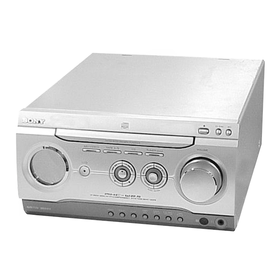
• HCD-WZ8D is the tuner, and the CD/
DVD player section in MHC-WZ8D.
TE
L 13942296513
CD/DVD player section
Laser
Frequency response
Signal-to-noise ratio
Dynamic range
Video color system format
DVD DIGITAL (OPTICAL) OUT (European, Russian
and Australian models only) (Square optical connector
jack, rear panel):
Tuner section
FM stereo, FM/AM superheterodyne tuner
FM tuner section
Tuning range
Russian model
Other models
Antenna
Antenna terminals
Intermediate frequency
www
.
Sony Corporation
9-877-415-01
2003G1678-1
Home Audio Company
© 2003.07
Published by Sony Engineering Corporation
http://www.xiaoyu163.com
AM tuner section
Semiconductor laser
Tuning range
(DVD: λ=650 nm,
Latin American model:
CD: λ=780 nm)
Emission duration:
continuous
DVD (PCM 48 kHz):
2 Hz – 22 kHz = (±1 dB)
CD: 2 Hz – 20 kHz =
European, Russian and Middle Eastern models:
(±1 dB)
More than 90 dB
More than 90 dB
Other models:
NTSC, PAL
Optical Wavelength:
660 nm
Antenna
Antenna terminals
Intermediate frequency
General
65.0 – 74.0 MHz
Power requirements
(There is no stereo effect)
Power voltage is DC 9V and fed with STEREO
87.5 – 108.0 MHz
CASSETTE DECK AMPLIFIER (DXA-WZ8D)
87.5 – 108.0 MHz
from the external SYSTEM CONTROL connectors.
FM lead antenna
75 ohms unbalanced
10.7 MHz
x
ao
u163
y
i
http://www.xiaoyu163.com
HCD-WZ8D
2 9
8
Model Name Using Similar Mechanism
DVD
DVD Mechanism Type
Section
Optical Pick-up Name
SPECIFICATIONS
Q Q
3
6 7
1 3
1 5
530 – 1,710 kHz
(with the tuning interval
set at 10 kHz)
531 – 1,710 kHz
(with the tuning interval
set at 9 kHz)
531 – 1,602 kHz
(with the tuning interval
set at 9 kHz)
531 – 1,602 kHz
(with the tuning interval
set at 9 kHz)
530 – 1,710 kHz
(with the tuning interval
set at 10 kHz)
AM loop antenna
External antenna terminal
450 kHz
co
.
9 4
2 8
AEP Model
UK Model
Australian Model
HCD-SA30
CDM77A-DVBU20
TDP022W
0 5
8
2 9
9 4
2 8
Power consumption
European and Russian models:
235 watts
0.3 watts (in Power Saving
Mode)
Other models:
260 watts
Dimensions (w/h/d)
Approx. 255 × 135 ×
CD/DVD player/Tuner:
355 mm
Mass
CD/DVD player/Tuner:
Approx. 3.0 kg
Supplied accessories:
Remote Commander (1)
Batteries (2)
AM loop antenna (1)
FM lead antenna (1)
Speaker pads (20)
Speaker cords (5)
Video cord (1)
Design and specifications are subject to change
without notice.
m
CD/DVD PLAYER TUNER
9 9
E Model
9 9
Advertisement
Table of Contents

Related Manuals for Sony HCD-WZ8D


Summary of Contents for Sony HCD-WZ8D
- Page 1 3 7 63 1515 0 SERVICE MANUAL AEP Model UK Model Ver 1.0 2003. 07 E Model Australian Model • HCD-WZ8D is the tuner, and the CD/ DVD player section in MHC-WZ8D. Model Name Using Similar Mechanism HCD-SA30 DVD Mechanism Type CDM77A-DVBU20 Section...
-
Page 2: Table Of Contents
HCD-WZ8D 3 7 63 1515 0 TABLE OF CONTENTS NOTES ON HANDLING THE OPTICAL PICK-UP BLOCK OR BASE UNIT 1. GENERAL ·········································································· 4 The laser diode in the optical pick-up block may suffer electrostatic 2. DISASSEMBLY break-down because of the potential difference generated by the 2-1. - Page 3 COMPONENTS IDENTIFIED BY MARK 0 OR DOTTED LINE WITH MARK 0 ON THE SCHEMATIC DIAGRAMS AND IN THE PARTS LIST ARE CRITICAL TO SAFE OPERATION. REPLACE THESE COMPONENTS WITH SONY PARTS WHOSE PART NUMBERS APPEAR AS SHOWN IN THIS MANUAL OR IN SUPPLEMENTS PUBLISHED BY SONY.
-
Page 4: General
HCD-WZ8D SECTION 1 GENERAL 3 7 63 1515 0 This section is extracted from instruction manual. List of button locations and reference pages Illustration number How to use this page TAPE A/B 3 (41, 42) Use this page to find the location of buttons and other parts of the system that are mentioned in the text. - Page 5 HCD-WZ8D 3 7 63 1515 0 Remote control ALPHABETICAL ORDER BUTTON DESCRIPTIONS ?/1 (power) 1 (10, 47) A – O P – Z m/M (rewind/fast forward) ALBUM – wa (14, 17, 19) PLAY MODE/DIRECTION ed qd (14, 36, 40)
-
Page 6: Hooking Up The System
HCD-WZ8D 3 7 63 1515 0 Getting Started Hooking up the system Perform the following procedures 1 to 7 to hook up your system using the supplied cords and accessories. European model is used for illustration purpose. To center... -
Page 7: Disassembly
HCD-WZ8D SECTION 2 DISASSEMBLY 3 7 63 1515 0 • The equipment can be removed using the following procedure. CASE FRONT PANEL ASSY PANEL BOARD, CD-TC SW BOARD, DVD MECHANISM 4CH-VOL BOARD, ENTER-SW BOARD, (CDM77B-DVBU20) VIDEO BOARD BACK LIGHT BOARD, LCD BOARD... -
Page 8: Front Panel Assy
HCD-WZ8D 3 7 63 1515 0 2-2. Front Panel Assy How to eject the disc tray when the main power cannot be turned on. 3 loading panel 5 wire (NO601) 4 screw q; wire (flat type) (+BVTP 3 × 8) -
Page 9: 4Ch-Vol Board, Video Board
HCD-WZ8D 3 7 63 1515 0 2-4. 4CH-VOL Board, VIDEO Board 2 wire (flat type) qd cord connector 3 seven screws (11/15 core) (CN107) (+BVTP 3 × 8) 7 two screws (+BVTP 3 × 8) 5 cord connector (CN302) -
Page 10: Dvd Mechanism (Cdm77A-Dvbu20)
HCD-WZ8D 3 7 63 1515 0 2-6. DVD Mechanism (CDM77A-DVBU20) 4 DVD mechanism (CDM77B-DVBU20) 2 three screws (+BVTP 3 × 8) 3 wire (flat type) (29 core) (RF board) 1 wire (flat type) (5 core) (CN103) L 13942296513 2-7. DMB03 Board... -
Page 11: Mic Board
HCD-WZ8D 3 7 63 1515 0 2-8. MIC Board 2 claw 1 two screws (+BVTP 3 × 8) 3 connector (CN701) 4 MIC board L 13942296513 2-9. Tray (AU) bottom side 3 two claws 4 tray (AU) u163 http://www.xiaoyu163.com... -
Page 12: Ms-128 Board
HCD-WZ8D 3 7 63 1515 0 2-10. MS-128 Board 1 belt 3 MS-128 board 2 four claws L 13942296513 2-11. Base Unit 1 belt 7 chuck cam 3 puley gear 4 driving gear 5 two claws 2 claw 6 base unit u163 http://www.xiaoyu163.com... -
Page 13: Pick-Up Unit (Tdp022W)
HCD-WZ8D 3 7 63 1515 0 2-12. Pick-up Unit (TDP022W) 6 holder (DBU1) 7 three insulators 1 claw 8 pick-up unit (TDP022W) 2 flexible board (CN003) 3 w ire (flat type) 5 three step screws (M) 24p (CN001) 4 RF board... -
Page 14: Test Mode
HCD-WZ8D SECTION 3 TEST MODE 3 7 63 1515 0 [Cold Reset] [Disc Tray Lock] • The cold reset clears all data including preset data stored in the • The disc tray lock function for the antitheft of an demonstration RAM to initial conditions. - Page 15 HCD-WZ8D 3 7 63 1515 0 • VACS Level Display Mode DVD OSD Test Mode Procedure: [GENERAL DESCRIPTION] 1. Press three buttons x , z START (REC PAUSE) and The Test Mode allows you to make diagnosis and adjustment easily TUNER/BAND simultaneously.
- Page 16 HCD-WZ8D 3 7 63 1515 0 • Example display 0-2-5. Region Model destination code is displayed. (2 digits number) ### Syscon Diagnosis ### 0-3. EEPROM Check 0-3-1. Sampling Check Diag All Check EEPROM check at every 64 words. No.2 Version It compares read data with write data of each address.
- Page 17 HCD-WZ8D 3 7 63 1515 0 1-1. DVD-SL (single layer) 24. Auto track gain adjust Press the [1] key on the remote commander and insert a DVD single Search Check layer disc following the message. Then the adjustment will be made 25.
- Page 18 HCD-WZ8D 3 7 63 1515 0 DRIVE MANUAL OPERATION 2-1. Disc Type Note: This mode is used for design, and not used in service fundamen- tally. Disc Type On the Test Mode Menu screen, press the key on the remote Disc Type Select commander, and the Operation Menu will be displayed.
- Page 19 HCD-WZ8D 3 7 63 1515 0 2-1-3. Disc Type CD 2-3. Track/Layer Jump It sets up so that it may judge as a disc type of specification of the disc with which the set was inserted. Track/Layer Jump : CD disc (normal speed, 12 cm)
- Page 20 HCD-WZ8D 3 7 63 1515 0 2-5. EEPROM Write Adjust 2-7. Disc Check Memory EEPROM Write Adjust Disc Check Memory 1. Focus Offset 1. SL Disc check 2. Focus Gain 2. CD Disc check 3. Trk. Offset Coarse 3. DL Disc check 4.
- Page 21 HCD-WZ8D 3 7 63 1515 0 MECHA AGING • Code list of Emergency History 10: Communication to RF AMP (IC001) failed. On the Test Mode Menu screen, selecting executes the aging of 11: Each servo for focus, tracking, and spindle is unlocked.
- Page 22 HCD-WZ8D 3 7 63 1515 0 aa: Initialization is completed or not. VERSION INFORMATION : Complete. On the Test Mode Menu screen, selecting displays the ROM other number : Not complete. version and region code. bb: Operating status of mechanism deck at an error occurred.
-
Page 23: Diagrams
HCD-WZ8D SECTION 4 3 7 6 3 1 5 1 5 0 THIS NOTE IS COMMON FOR PRINTED WIRING BOARDS AND SCHEMATIC DIAGRAMS. DIAGRAMS (In addition to this, the necessary note is printed in each block.) Note on Schematic Diagram:... - Page 24 HCD-WZ8D 3 7 6 3 1 5 1 5 0 • Waveforms -RF Board- IC001 1 (DVDRFP) IC001 el (TE) IC001 r; (FE) IC001 tj (RFAC) 0.3 Vp-p 0.5 Vp-p 800 mVp-p 1.3 Vp-p 200 mV/DIV, 100 ns/DIV 500 mV/DIV, 1 ms/DIV...
-
Page 25: Block Diagrams - Rf Servo Section
HCD-WZ8D 4–1. Block Diagrams – RF Servo Section – 3 7 6 3 1 5 1 5 0 AEP, UK, RU, AUS CD_DOUT VIDEO SECTION 117 RFIN SD0 – SD7 VIDEO DOUT SECTION DVDRFP ATOP RFAC 50 RFAC RFSIN... -
Page 26: Video Section
HCD-WZ8D – Video Section – 3 7 6 3 1 5 1 5 0 IC801 VIDEO AMP, 75Ω DRIVER IC256 RF SERVO J802 V OUTA D-FF SECTION VOUT V OUTB VIDEO OUT 4 V IN VDAC_0 • SIGNAL PATH... -
Page 27: Audio Section
HCD-WZ8D – Audio Section – 3 7 6 3 1 5 1 5 0 AEP, UK, RU, E2 VIDEO SECTION IC302 IC301 D/A CONVERTER SOUND PROCESSOR EXCEPT AEP, UK, RU, E2 IC601 DATA0 (DMX-B) 31 DATA4 VOUT1 41 FL-IN... -
Page 28: Main Section
HCD-WZ8D – Main Section – 3 7 6 3 1 5 1 5 0 IC101 SOUND PROCESSOR J101(2/2) J101(1/2) IND2 REC A2 MD(VIDEO) MD(VIDEO) INB2 AUDIO Q270 DOWNMIX-L R-CH R-CH INC2 MUTE SECTION R-CH HEADPHONE AMP AUDIO ANALOG-IN-L R-CH... -
Page 29: Printed Wiring Board - Rf Board
HCD-WZ8D 4–2. Printed Wiring Board – RF Board – • : Uses unleaded solder. • See page 23 for Circuit Boards Location. 3 7 6 3 1 5 1 5 0 RF BOARD RF BOARD (SIDE A) (SIDE B) •... -
Page 30: Schematic Diagram - Rf Board
HCD-WZ8D 4–3. Schematic Diagram – RF Board – • See page 24 for Waveforms. • See page 55 for IC Block Diagrams. 3 7 6 3 1 5 1 5 0 C006 C028 C027 R026 C013 C031 1000p CN002 C030 0.01... -
Page 31: Q Q 4-4. Printed Wiring Board - Dmb03 Board (Side A)
HCD-WZ8D 4–4. Printed Wiring Board – DMB03 Board (Side A) – • : Uses unleaded solder. • See page 23 for Circuit Boards Location. 3 7 6 3 1 5 1 5 0 MAIN BOARD MAIN BOARD VIDEO BOARD... -
Page 32: Printed Wiring Board - Dmb03 Board (Side B)
HCD-WZ8D 4–5. Printed Wiring Board – DMB03 Board (Side B) – • : Uses unleaded solder. • See page 23 for Circuit Boards Location. 3 7 6 3 1 5 1 5 0 IC352 (EXCEPT AEP,UK,RU,E2) C610 C609 • Semiconductor... -
Page 33: Schematic Diagram - Dmb03 Board (1/9)
HCD-WZ8D 4–6. Schematic Diagram – DMB03 Board (1/9) – • See page 56 for IC Block Diagrams. 3 7 6 3 1 5 1 5 0 (1/9) (6/9,9/9) (Page 38,41) (4 /9) CN107 25P(AEP,UK,RU,AUS) AUDIO_DGND 21P(EXCEPT AEP,UK,RU,AUS) R309 CN107 CL309 AUDIO_D2.5V... -
Page 34: Schematic Diagram - Dmb03 Board (2/9)
HCD-WZ8D 4–7. Schematic Diagram – DMB03 Board (2/9) – • See page 57 for IC Block Diagrams. 3 7 6 3 1 5 1 5 0 (2/9) R587 CL505 CL504 CL503 CL502 FL502 C567 CL501 C568 R569 R545 C522... -
Page 35: Schematic Diagram - Dmb03 Board (3/9)
HCD-WZ8D 4–8. Schematic Diagram – DMB03 Board (3/9) – • See page 58 for IC Block Diagrams. 3 7 6 3 1 5 1 5 0 (3/9) IC703(2/2) R784 C701 R786 NJM3404AV( 100k TE2) R700 TP703 R787 100k 8.2k C782 0.0015... -
Page 36: Schematic Diagram - Dmb03 Board (4/9)
HCD-WZ8D 4–9. Schematic Diagram – DMB03 Board (4/9) – 3 7 6 3 1 5 1 5 0 (2 /9) (4/9) JL521 C527 0.01 C526 R543 R547 (5 /9) R581 R580 R589 (6 /9) C519 0.01 (1 /9,7/9) 33, 39 R579 8.2k... -
Page 37: Schematic Diagram - Dmb03 Board (5/9)
HCD-WZ8D 4–10. Schematic Diagram – DMB03 Board (5/9) – • See page 24 for Waveforms. • See page 58 for IC Block Diagrams. 3 7 6 3 1 5 1 5 0 (3 /9) (5/9) CD_DOUT (7 /9) (6 /9) -
Page 38: Schematic Diagram - Dmb03 Board (6/9)
HCD-WZ8D 4–11. Schematic Diagram – DMB03 Board (6/9) – 3 7 6 3 1 5 1 5 0 (6/9) CN202 (3/9) (Page 35) (7/9) (Page 39) (5/9) CN105 (Page 37) VIDEO SW VMUTE IC255 TC7S00FU (TE85R) (1/9,9/9) (Page 33, 41) -
Page 39: Schematic Diagram - Dmb03 Board (7/9)
HCD-WZ8D 4–12. Schematic Diagram – DMB03 Board (7/9) – • See page 24 for Waveforms. 3 7 6 3 1 5 1 5 0 (6/9) (5/9) (7/9) CD_DOUT R265 R266 R267 R263 R264 IC252 SWITCHING R225 R226 R228 R251... -
Page 40: Schematic Diagram - Dmb03 Board (8/9)
HCD-WZ8D 4–13. Schematic Diagram – DMB03 Board (8/9) – • See page 57 for IC Block Diagrams. 3 7 6 3 1 5 1 5 0 (8/9) IC203 HY57V283220T-6 C218 0.01 C255 10 10V F C220 0.01 C259 FL203... -
Page 41: Schematic Diagram - Dmb03 Board (9/9)
HCD-WZ8D 4–14. Schematic Diagram – DMB03 Board (9/9) – • See page 24 for Waveforms. 3 7 6 3 1 5 1 5 0 C617 C616 C611 C610 C612 R633 C609 IC602 IS61LV6416- 10TT(ISSI) 1 3 9 4 2 2 9 6 5 1 3... -
Page 42: Printed Wiring Board - Main Section
HCD-WZ8D 4–15. Printed Wiring Board – Main Section – • : Uses unleaded solder. • See page 23 for Circuit Boards Location. 3 7 6 3 1 5 1 5 0 (EXCEPT AEP,UK,RU,E2) 4CH-VOL (FOR JIG) DMB03 BOARD DMB03... -
Page 43: Schematic Diagram - Main Section (1/2)
HCD-WZ8D 4–16. Schematic Diagram – Main Section (1/2) – • See page 59 for IC Block Diagrams. 3 7 6 3 1 5 1 5 0 CN104 CN105 R277 Q274 Q275 DTA114EKA DTC114EKA C272 C271 Q272 DTA114EKA J101 C173... -
Page 44: Schematic Diagram - Main Section (2/2)
HCD-WZ8D 4–17. Schematic Diagram – Main Section (2/2) – • See page 24 for Waveforms. • See page 59 for IC Block Diagrams. 3 7 6 3 1 5 1 5 0 Q276 DTA114EKA CN107 R279 Q277 C403 C114... -
Page 45: Printed Wiring Board - Panel Board
HCD-WZ8D 4–18. Printed Wiring Board – PANEL Board – • : Uses unleaded solder. • See page 23 for Circuit Boards Location. 3 7 6 3 1 5 1 5 0 • Semiconductor Location Ref. No. Location D606 D605... -
Page 46: Schematic Diagram - Panel Board
HCD-WZ8D 4–19. Schematic Diagram – PANEL Board – 3 7 6 3 1 5 1 5 0 D606 D605 D604 D603 D602 SEL5E23C SEL5E23C SEL5E23C SEL5E23C SEL5423E D601 SEL5223S C606 C605 C604 C603 0.001 0.001 0.001 0.001 Q608,609,611 NO805... -
Page 47: Printed Wiring Board - Lcd/Switch Section
HCD-WZ8D 4–20. Printed Wiring Board – LCD/Switch Section – • : Uses unleaded solder. • See page 23 for Circuit Boards Location. 3 7 6 3 1 5 1 5 0 D610 D609 • Semiconductor 1 3 9 4 2 2 9 6 5 1 3 Location Ref. -
Page 48: Schematic Diagram - Lcd/Switch Section
HCD-WZ8D 4–21. Schematic Diagram – LCD/Switch Section – 3 7 6 3 1 5 1 5 0 LCD201 CN601 D608-613 C623 D610 AMP-L 0.001 SELU6614C J603 C608 C611 C622 D608 D611 D612 D613 0.001 0.001 0.001 D609 SELS6E14C SELS6D14C... -
Page 49: Printed Wiring Board - Regulator Board
HCD-WZ8D 4–22. Printed Wiring Board – REGULATOR Board – • : Uses unleaded solder. • See page 23 for Circuit Boards Location. 3 7 6 3 1 5 1 5 0 • Semiconductor Location IC501 Ref. No. Location D581... -
Page 50: Schematic Diagram - Regulator Board
HCD-WZ8D 4–23. Schematic Diagram – REGULATOR Board – • See page 59 for IC Block Diagrams. 3 7 6 3 1 5 1 5 0 IC501 BA3308 C522 R509 C521 R559 R510 CN503 Q552 C523 R500 2SC3624A R563 C559... -
Page 51: Printed Wiring Board - 4Ch-Vol Board
HCD-WZ8D 4–24. Printed Wiring Board – 4CH-VOL Board – • : Uses unleaded solder. • See page 23 for Circuit Boards Location. 3 7 6 3 1 5 1 5 0 CN303 DMB03 (AEP,UK,RU,AUS) BOARD (EXCEPT AEP,UK,RU,AUS) CN107 (Page 31) -
Page 52: Schematic Diagram - 4Ch-Vol Board
HCD-WZ8D 4–25. Schematic Diagram – 4CH-VOL Board – 3 7 6 3 1 5 1 5 0 CN301 CN303 JW305 C346 R301 C347 C348 C315 C334 C331 C365 R302 R303 C302 220p IC301 M61530FP-D60G C370 1 3 9 4 2 2 9 6 5 1 3... -
Page 53: Printed Wiring Board - Video/Mic Board
HCD-WZ8D 4–26. Printed Wiring Board – VIDEO/MIC Board – • : Uses unleaded solder. • See page 23 for Circuit Boards Location. 3 7 6 3 1 5 1 5 0 DMB03 BOARD (EXCEPT AEP,UK,RU) CN105 (Page 31) (EXCEPT E2) -
Page 54: Schematic Diagram - Video/Mic Board
HCD-WZ8D 4–27. Schematic Diagram – VIDEO/MIC Board – • See page 24 for Waveforms. 3 7 6 3 1 5 1 5 0 R724 C729 0.22 J702 R742 C721 100p R718 150k IC702(1/2) R727 C732 IC702(2/2) NJM4580MD C727 R719... -
Page 55: Ic Block Diagrams
HCD-WZ8D 3 7 63 1515 0 4-28. IC Block Diagrams IC001 CXD1881AR (RF Board) 64 63 62 61 60 59 55 54 53 52 FAST ATTACK INPUT OUTPUT HOLD FULL WAVE AGC CHARGE INHIBIT RECTIFER PUMP PROGRAMMABLE FROM S-PORT... - Page 56 HCD-WZ8D 3 7 63 1515 0 IC302 PCM1609KPTR (DMB03 Board) Power Supply System Clock VCC3 SCKI Manager SCKO Output Amp and AGND3 Low-pass Filter VCC4 Output Amp and Low-pass Filter AGND4 Enhanced Output Amp and Oversampling Multi-level LRCK Low-pass Filter...
- Page 57 HCD-WZ8D 3 7 63 1515 0 IC216 SN74ALVCH16841DGGR (DMB03 BOARD) 56 1LE LATCH 1D10 1Q10 IC509 CXD3068Q (DMB03 Board) LATCH L 13942296513 2D10 2Q10 29 2LE u163 http://www.xiaoyu163.com...
- Page 58 HCD-WZ8D 3 7 63 1515 0 IC706 MSM51V18165F-60TSKR1 (DMB03 Board) 40 – 36 34 33 REFRESH INTERNAL TIMING CONTROL ADDRESS GENERATOR CLOCK COUNTER CONTROLLER OUTPUT INPUT BUFFER BUFFER COLUMN CONTROLLER ADDRESS ADDRESS BUFFERS BUFFERS SENSE COLUMN AMPLIFIER DECODERS OUTPUT...
- Page 59 HCD-WZ8D 3 7 63 1515 0 IC904 TC7W74FK-TE85L (DMB03 Board) IC202 BA6956AN (MAIN Board) CONTROL LOGIC IC903 SI-8033JF (REGULATOR Board) IC913 SI-8050JF (REGULATOR Board) OVER OVER REGULATOR CURRENT REGULATOR CURRENT PROTECTOR PROTECTOR LATCH LATCH RESET RESET L 13942296513 &...
- Page 60 HCD-WZ8D 3 7 63 1515 0 IC801 MM1568AJBE (VIDEO Board) VCC2 VCC1 BIAS 75Ω COUT DRIVER MUTE1 CLAMP GND2 75Ω VOUT DRIVER YC MIX VSAG CLAMP GND2 75Ω YOUT DRIVER BIAS BIAS YSAG GND1 GND1 10 NC 11 GND2 CYIN 12 75Ω...
-
Page 61: Ic Pin Function Description
HCD-WZ8D 3 7 63 1515 0 4-29. IC Pin Function Description • IC207 ZIVA5X-C1F (DVD SYSTEM PROCESSOR)(DMB03 BOARD) Pin No. Pin Name Description VDDP — Power supply terminal (+3.3V)(I/O signal) Address bus HAD15 Data bus (address signal multiplexed) HAD14... - Page 62 HCD-WZ8D 3 7 63 1515 0 Pin No. Pin Name Description MRAS SDRAM row address strobe signal output MCAS SDRAM column address strobe signal output SDRAM write enable signal output (“H” : read, “L” : write) GND25 — Ground terminal (SDRAM I/O signal) VDD25 —...
- Page 63 HCD-WZ8D 3 7 63 1515 0 Pin No. Pin Name Description MD30 SDRAM data MD31 SDRAM data GND25 — Ground terminal (SDRAM I/O signal) VDD25 — Power supply terminal (+3.3V)(SDRAM I/O signal) VCLK System clock (not used) XCK_I/O_SEL 5.1ch/downmix switch signal output...
- Page 64 HCD-WZ8D 3 7 63 1515 0 Pin No. Pin Name Description DATA1(FLR) Audio data(Front L/R signal) output VDDP — Power supply terminal (+3.3V)(I/O signal) GNDP — Ground terminal (I/O signal) DATA2(SLR) Audio data(Rear L/R signal) output DATA3(CSW) Audio data(Center/Subwoofer signal) output...
- Page 65 HCD-WZ8D 3 7 63 1515 0 Pin No. Pin Name Description TCK signal input RESET ZIVA reset input BUS CLK Not used — Ground terminal (inside core) — Power supply terminal (+1.8V)(inside core) Address bus 3 Address bus 2 GNDP —...
- Page 66 HCD-WZ8D 3 7 63 1515 0 • IC401 M30622MGN-B22FP (AEP, UK, RU, E2, MX) , -B12FP (EXCEPT AEP, UK, RU, E2, MX)(SYSTEM CONTROL)(MAIN BOARD) Pin No. Pin Name Description MIC-CHECK Microphone detection signal input NO USE — Not used NO USE —...
- Page 67 HCD-WZ8D 3 7 63 1515 0 Pin No. Pin Name Description VOL-CLK Clock output to the audio signal processor (IC101) VOL-DATA Data output to the audio signal processor (IC101) CN CHECK Connection check signal input (from DXA-WZ8D) AMS-IN AMS signal input (“L” : in, “H” : off)(from DXA-WZ8D) TC LINE-MUTE TC line muting signal output (“H”...
- Page 68 HCD-WZ8D 3 7 63 1515 0 • IC901 CXP973064-226R (MECHANISM CONTROLLER)(DMB03 BOARD) Pin No. Pin Name Description NO USE Not used SDEN Serial data enable signal output to DVD/CD RF amplifier DOCTRL/ Digital out on/off control signal output to the digital signal processor ISBTEST “L”: digital out off, “H”: digital out on...
- Page 69 HCD-WZ8D 3 7 63 1515 0 Pin No. Pin Name Description CONTROL 2 Disc tray out detection signal input terminal Not used GFS DVD Guard frame sync signal input from the DVD decoder MUTE CD Muting on/off control signal output to the digital signal processor “H”: muting on MUTE 2D Muting on/off control signal output to the motor/coil driver “H”: muting on...
-
Page 70: Exploded Views
HCD-WZ8D SECTION 5 EXPLODED VIEWS 3 7 63 1515 0 NOTE: • -XX, -X mean standardized parts, so they may have • Abbreviation : Russian model some differences from the original one. AUS : Australian model : Singapore model •... -
Page 71: Chassis Section
HCD-WZ8D 3 7 63 1515 0 5-2. Chassis Section (1/2) not supplied not supplied not supplied L 13942296513 not supplied Ref. No. Part No. Description Remarks Ref. No. Part No. Description Remarks 4-238-994-11 KNOB (MIC) 3-970-608-01 SUMITITE (B3), +BV... - Page 72 HCD-WZ8D 3 7 63 1515 0 Chassis Section (2/2) not supplied not supplied L 13942296513 not supplied not supplied Ref. No. Part No. Description Remarks Ref. No. Part No. Description Remarks 1-693-604-11 TUNER (FM/AM)(AEP, UK) A-4732-332-A 4CH-VOL BOARD, COMPLETE (AUS)
-
Page 73: Dvd Mechanism Deck Section
HCD-WZ8D 3 7 63 1515 0 5-3. DVD Mechanism Section M001 L 13942296513 not supplid Ref. No. Part No. Description Remarks Ref. No. Part No. Description Remarks 4-243-742-01 TRAY (AU) 3-053-847-31 INSULATOR 3-080-484-01 DRIVING GEAR 1-689-264-11 PWB, FLEXIBLE 0 412... -
Page 74: Electrical Parts List
HCD-WZ8D SECTION 6 4CH-VOL ELECTRICAL PARTS LIST 3 7 63 1515 0 NOTE: • Due to standardization, replacements in the • CAPACITORS: KR : Korean model uF: µF parts list may be different from the parts MY : Malaysia model specified in the diagrams or the components •... - Page 75 HCD-WZ8D 4CH-VOL BACK LIGHT 3 7 63 1515 0 Ref. No. Part No. Description Remarks Ref. No. Part No. Description Remarks < TRANSISTOR > R374 1-216-845-11 METAL CHIP 100K 1/10W R375 1-216-821-11 METAL CHIP 1/10W Q301 8-729-141-73 TRANSISTOR 2SC3624A-T1L15L16...
- Page 76 HCD-WZ8D BACK LIGHT CD-TC SW DMB03 3 7 63 1515 0 Ref. No. Part No. Description Remarks Ref. No. Part No. Description Remarks R694 1-216-820-11 METAL CHIP 1/10W C249 1-164-947-11 CERAMIC CHIP 0.01uF R695 1-216-820-11 METAL CHIP 1/10W C250 1-164-947-11 CERAMIC CHIP 0.01uF...
- Page 77 HCD-WZ8D DMB03 3 7 63 1515 0 Ref. No. Part No. Description Remarks Ref. No. Part No. Description Remarks C368 1-164-935-11 CERAMIC CHIP 470PF 10.00% 50V C573 1-164-874-11 CERAMIC CHIP 100PF 5.00% 50V C392 1-126-395-11 ELECT 22uF C588 1-164-939-11 CERAMIC CHIP 0.0022uF 10.00% 50V...
- Page 78 HCD-WZ8D DMB03 3 7 63 1515 0 Ref. No. Part No. Description Remarks Ref. No. Part No. Description Remarks C720 1-125-777-11 CERAMIC CHIP 0.1uF 10.00% 10V C918 1-164-947-11 CERAMIC CHIP 0.01uF C924 1-164-947-11 CERAMIC CHIP 0.01uF C721 1-107-820-11 CERAMIC CHIP 0.1uF...
- Page 79 HCD-WZ8D DMB03 3 7 63 1515 0 Ref. No. Part No. Description Remarks Ref. No. Part No. Description Remarks FL602 1-234-177-21 FERRITE JW804 1-218-990-11 SHORT CHIP (E3, E15, EA, MY, SP, TH, KR, PH, AUS) JW805 1-218-990-11 SHORT CHIP...
- Page 80 HCD-WZ8D DMB03 3 7 63 1515 0 Ref. No. Part No. Description Remarks Ref. No. Part No. Description Remarks R244 1-216-821-11 METAL CHIP 1/10W R327 1-216-864-11 METAL CHIP 1/10W R245 1-216-829-11 METAL CHIP 4.7K 1/10W R328 1-216-864-11 METAL CHIP...
- Page 81 HCD-WZ8D DMB03 3 7 63 1515 0 Ref. No. Part No. Description Remarks Ref. No. Part No. Description Remarks R561 1-216-821-11 METAL CHIP 1/10W R615 1-216-864-11 METAL CHIP 1/10W R562 1-216-821-11 METAL CHIP 1/10W R616 1-216-809-11 METAL CHIP 1/10W...
- Page 82 HCD-WZ8D DMB03 3 7 63 1515 0 Ref. No. Part No. Description Remarks Ref. No. Part No. Description Remarks R730 1-216-801-11 METAL CHIP 1/10W R913 1-216-833-11 METAL CHIP 1/10W R731 1-216-801-11 METAL CHIP 1/10W R915 1-216-809-11 METAL CHIP 1/10W...
- Page 83 HCD-WZ8D DMB03 ENTER-SW HP AMP MAIN 3 7 63 1515 0 Ref. No. Part No. Description Remarks Ref. No. Part No. Description Remarks R1803 1-164-156-11 CERAMIC CHIP 0.1uF < JACK > R9980 1-216-864-11 METAL CHIP 1/10W R9981 1-216-864-11 METAL CHIP...
- Page 84 HCD-WZ8D MAIN 3 7 63 1515 0 Ref. No. Part No. Description Remarks Ref. No. Part No. Description Remarks C108 1-126-964-11 ELECT 10uF 20.00% 50V C254 1-126-964-11 ELECT 10uF 20.00% 50V C255 1-164-156-11 CERAMIC CHIP 0.1uF C109 1-110-563-11 CERAMIC CHIP 0.068uF...
- Page 85 HCD-WZ8D MAIN 3 7 63 1515 0 Ref. No. Part No. Description Remarks Ref. No. Part No. Description Remarks < TERMINAL > R104 1-216-819-11 METAL CHIP 1/10W R105 1-216-845-11 METAL CHIP 100K 1/10W EP102 1-537-738-21 TERMINAL, GROUND R106 1-216-864-11 METAL CHIP 1/10W <...
- Page 86 HCD-WZ8D MAIN 3 7 63 1515 0 Ref. No. Part No. Description Remarks Ref. No. Part No. Description Remarks R273 1-216-813-11 METAL CHIP 1/10W R433 1-216-809-11 METAL CHIP 1/10W R274 1-216-821-11 METAL CHIP 1/10W R434 1-216-833-11 METAL CHIP 1/10W...
- Page 87 HCD-WZ8D MAIN 3 7 63 1515 0 Ref. No. Part No. Description Remarks Ref. No. Part No. Description Remarks R490 1-216-809-11 METAL CHIP 1/10W C712 1-136-167-00 FILM 0.15uF 5.00% 50V R491 1-216-809-11 METAL CHIP 1/10W (E3, E15, EA, MY, SP, KR, TH, PH, AUS)
- Page 88 HCD-WZ8D MS-128 PANEL 3 7 63 1515 0 Ref. No. Part No. Description Remarks Ref. No. Part No. Description Remarks < JACK > R742 1-216-833-11 METAL CHIP 1/10W (E3, E15, EA, MY, SP, KR, TH, PH, AUS) J701 1-770-226-11 JACK (LARGE TYPE)(MIC1) (EXCEPT AEP, UK, RU) <...
- Page 89 HCD-WZ8D PANEL REGULATOR 3 7 63 1515 0 Ref. No. Part No. Description Remarks Ref. No. Part No. Description Remarks < TRANSISTOR > R675 1-216-821-11 METAL CHIP 1/10W R676 1-216-821-11 METAL CHIP 1/10W Q601 8-729-900-53 TRANSISTOR DTC114EKA-T146 R678 1-216-864-11 METAL CHIP...
- Page 90 HCD-WZ8D REGULATOR 3 7 63 1515 0 Ref. No. Part No. Description Remarks Ref. No. Part No. Description Remarks C586 1-162-945-11 CERAMIC CHIP 22PF IC581 8-759-100-96 IC NJM4558M-TE2 IC901 8-759-701-59 IC TA7809S C587 1-130-483-00 MYLAR 0.01uF IC902 8-759-701-59 IC TA7809S...
- Page 91 HCD-WZ8D REGULATOR 3 7 63 1515 0 Ref. No. Part No. Description Remarks Ref. No. Part No. Description Remarks R509 1-216-836-11 METAL CHIP 1/10W A-4728-690-A RF BOARD, COMPLETE R510 1-216-816-11 METAL CHIP 1/10W ******************* R511 1-216-839-11 METAL CHIP 1/10W <...
- Page 92 HCD-WZ8D VIDEO 3 7 63 1515 0 Ref. No. Part No. Description Remarks Ref. No. Part No. Description Remarks < COIL > C809 1-126-960-11 ELECT 20.00% 50V C810 1-126-960-11 ELECT 20.00% 50V L001 1-412-031-11 INDUCTOR CHIP 47uH L002 1-412-031-11 INDUCTOR CHIP 47uH...
- Page 93 HCD-WZ8D VIDEO 3 7 63 1515 0 Ref. No. Part No. Description Remarks R806 1-218-284-11 METAL CHIP 1/10W R807 1-218-284-11 METAL CHIP 1/10W R808 1-218-284-11 METAL CHIP 1/10W R809 1-218-285-11 METAL CHIP 1/10W R810 1-218-285-11 METAL CHIP 1/10W ************************************************************...
- Page 94 HCD-WZ8D 3 7 63 1515 0 REVISION HISTORY Clicking the version allows you to jump to the revised page. Also, clicking the version at the upper right on the revised page allows you to jump to the next revised page.
Need help?
Do you have a question about the HCD-WZ8D and is the answer not in the manual?
Questions and answers