Table of Contents
Advertisement
SERVICE MANUAL
Ver 1.3 2003.12
HCD-S888 is the amplifier, DVD/CD player and
tuner section in DAV-S888.
This system incorporates with Dolby* Digital and Dolby Pro Loic (II)
adaptive matrix surround decoder and the DTS** Digital Surround System.
* Manufactured under license from Dolby Laboratories.
"Dolby", "Pro Logic" and the double-D symbol are trademarks of Dolby
Laboratories.
** Man ufactured under license from Digital Theater Systems, Inc.
"DTS" and "DTS Digital Surround" are trademarks of Digital Theater Systems, Inc.
Amplifier section
Stereo mode
100 W + 100 W (3 ohms at 1 kHz, THD 10 %)
Surround mode
Front: 100 W + 100 W
Center*: 100 W
Rear*: 100 W + 100 W
(3 ohms at 1 kHz, THD 10 %)
*Depending on the sound field settings and the source, there may be no
sound output.
Inputs (Analog)
VIDEO 1, 2 : Sensitivity : 150 mV
Inputs (Digital)
VIDEO 2 (optical) : Sensitivity : –
Outputs (Analog)
VIDEO 1 (AUDIO OUT) : Voltage : 2V
PHONES :
Accepts low-and high-impedance headphones
Super Audio CD/DVD system
Laser
Semiconductor laser
(Super Audio CD/DVD: λ = 650 nm)
(CD: λ = 780 nm)
Emission duration: continuous
Signal format system
NTSC or NTSC/PAL
Frequency response (at 2 CH STEREO mode)
DVD (PCM): 2 Hz to 22 kHz (±1.0 dB)
CD: 2 Hz to 20 kHz (±1.0 dB)
Signal-to-noise ratio
More than 80 dB
(VIDEO 1 (AUDIO) connectors only)
Harmonic distortion
Less than 0.03 %
Sony Corporation
9-877-205-04
2003L16-1
Home Audio Company
© 2003.12
Published by Sony Engineering Corporation
SPECIFICATIONS
Impedance : 50 kilohms
Impedance : 1 kilohms
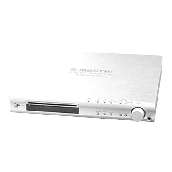
HCD-S888
Model Name Using Similar Mechanism
Mechanism Type
Base Unit Name
Optical Pick-up Name
FM tuner section
System
PLL quartz-locked digital synthesizer system
Tuning range
87.5 – 108.0 MHz (50 kHz step)
Antenna
FM wire antenna
Antenna terminals
75 ohms, unbalanced
Intermediate frequency 10.7 MHz
AM tuner section
System
PLL quartz-locked digital synthesizer system
Tuning range
European model:
531 – 1,602 kHz (with the interval set at 9 kHz)
Other models:
531 – 1,602 kHz (with the interval set at 9 kHz)
530 – 1,710 kHz (with the interval set at 10 kHz)
Antenna
Loop antenna
Intermediate frequency 450 KHz
Video section
Inputs
Video: 1 Vp-p 75 ohms
Outputs
Video: 1 Vp-p 75 ohms
S video:
Y: 1 Vp-p 75 ohms
C: 0.286 Vp-p 75 ohms
COMPONENT:
Y: 1 Vp-p 75 ohms
P
/C
B
B
COMPACT AV SYSTEM
AEP Model
UK Model
HCD-S880
CDM72B-DVBU12
DVBU12
TDP022W
, P
/C
: 0.7 Vp-p 75 ohms
R
R
– Continued on next page –
Advertisement
Table of Contents

Related Manuals for Sony HCD-S888


Summary of Contents for Sony HCD-S888
-
Page 1: Service Manual
HCD-S888 SERVICE MANUAL AEP Model UK Model Ver 1.3 2003.12 HCD-S888 is the amplifier, DVD/CD player and tuner section in DAV-S888. This system incorporates with Dolby* Digital and Dolby Pro Loic (II) Model Name Using Similar Mechanism HCD-S880 adaptive matrix surround decoder and the DTS** Digital Surround System. -
Page 2: Self Diagnosis Function
LINE WITH MARK 0 ON THE SCHEMATIC DIAGRAMS AND IN THE PARTS LIST ARE CRITICAL TO SAFE OPERATION. REPLACE THESE COMPONENTS WITH SONY PARTS WHOSE PART NUMBERS APPEAR AS SHOWN IN THIS MANUAL OR IN SUPPLEMENTS PUB- LISHED BY SONY. -
Page 3: Table Of Contents
HCD-S888 TABLE OF CONTENTS SELF DIAGNOSIS FUNCTION 6-13. Schematic Diagrams – DVD Board (5/10) – ..43 ........6-14. Schematic Diagrams – DVD Board (6/10) – ..44 6-15. Schematic Diagrams – DVD Board (7/10) – ..45 SERVICING NOTES .......... -
Page 4: Servicing Notes
HCD-S888 SECTION 1 SERVICING NOTES RELEASING THE DISC SLOT LOCK NOTES ON HANDLING THE OPTICAL PICK-UP The disc slot lock function for the antitheft of an demonstration BLOCK OR BASE UNIT disc in the store is equipped. The laser diode in the optical pick-up block may suffer electro-... -
Page 5: General
HCD-S888 SECTION 2 GENERAL This section is extracted from instruction manual. Location Of Controls Front Panel STANDBY FUNCTION BAND DISPLAY PHONES 1 POWER switch 9 PHONES jack 2 STANDBY indicator q; VOLUME control 3 Disc slot qa SOUND FIELD –/+... - Page 6 HCD-S888 Front Panel Display When playing back a DVD Lights up when you can Current chapter number Current sound Playing status TITLE CHAPTER ANGLE DIGITAL REPEAT 1 PRO LOGIC Current title Playing time Current repeat mode Current surround format number...
- Page 7 HCD-S888 1 TV [/1 (on/standby) Remote 2 Z (EJECT) 3 NAME 4 STEREO/MONO 5 MEMORY 6 CLEAR 7 PLAY MODE 8 AUDIO 9 ANGLE q; SUBTITLE qa VOL +/– qs ./> PREV/NEXT, TV CH –/+, PRESET –/+ > 10 10/0...
-
Page 8: Disassembly
HCD-S888 SECTION 3 DISASSEMBLY • This set can be disassembled in the order shown below. 3-1. Disassembly Flow FRONT PANELSECTION, SIDE PANEL (L)/(R) I/O BOARD POWER BOARD AMP BOARD SEL BOARD DVD BOARD MECHANISM DECK SECTION (CDM72B-DVBU12) POWER S/W BOARD,... -
Page 9: Front Panel Section, Side Panel (L)/(R)
HCD-S888 Note: Follow the disassembly procedure in the numerical order given. 3-2. Front Panel Section, Side Panel (L)/(R) 9 front panel section 0 two screws 4 connector (CN900) (BVTP3 × 8) qa side panel (L) 1 three screws (BVTP3 × 8) -
Page 10: Sel Board
HCD-S888 3-4. SEL Board 5 SEL board 3 screw 2 claw (DIA. 2.6 × 8) 4 retainer 1 screw (DIA. 2.6 × 8) 3-5. DVD Board 1 flexible flat cable qa two screws (BVTP3 × 8) (CN005) 5 flexible board... -
Page 11: Mechanism Deck Section (Cdm72B-Dvbu12)
HCD-S888 3-6. Mechanism Deck Section (CDM72B-DVBU12) 1 flexible flat cable (CN701) 3 mechanism deck (CDM72B-DVBU12) 2 four screws (BVTP3 × 8) 3-7. POWER S/W Board, DDCON Board 6 four screws (BTP2 × 6) 7 POWER S/W board 2 four screws 5 power button section (BVTP3 ×... -
Page 12: Power Board
HCD-S888 3-8. POWER Board 2 connector (CN903) 3 connector (CN902) 4 three screws 1 connector (BVTP3 × 8) (CN904) 6 power sheet 9 POWER board 5 screw 8 power sheet (BVTP3 × 8) 3-9. AMP Board 4 three screws 2 connector (BVTP3 ×... -
Page 13: Optical Pick-Up Block (Dvbu12)
HCD-S888 3-10. Optical Pick-up Block (DVBU12) 2 optical pick-up block (DVBU12) 1 screw (PTPWHM2.6) 3-11. RELAY Board 7 connector (CN702) 9 RELAY board 8 connecter (CN706) 4 two screws (BTP2.6 × 6) 6 two connector (CN703, 707) 3 connector (CN741) -
Page 14: Holder (At) Assy, Retainer (Chassis) Block
HCD-S888 3-12. Holder (AT) Assy, Retainer (Chassis) Block 2 three screws (BTP2.6 × 8) 3 holder (AT) assy 4 four screws (BTP2.6 × 6) 1 tension spring (S5) 5 retainer (chassis) block 3-13. Belt (L2) 1 two gears (S1) 2 belt (L2) -
Page 15: Pulley (Rtr) Assy
HCD-S888 3-14. Pulley (RTR) Assy 1 Rotate the pulley (RTR) assy in the direction of arrow A to disengage the shaft of the pulley (RTR) assy from the hole of the chassis (refer to fig. 1), and remove it. 2 gear (L4) -
Page 16: Pulley (Spt) Assy
HCD-S888 3-16. Pulley (SPT) Assy 2 pulley (SPT) assy 3 gear (S2) 4 torsion spring (72) 5 gear (SPT) 6 gear (KT) hole shaft (pulley (SPT) assy 1 Rotate the pulley (SPT) assy to fit position of the shaft to the hole of the chassis. -
Page 17: Assembly
HCD-S888 SECTION 4 ASSEMBLY • This set can be assembled in the order shown below. 4-1. How To Install Pulley (SPT) Assy 5 pulley (SPT) assy 4 gear (S2) 3 torsion spring (72) (Note) gear (S2) 2 gear (SPT) gear (SPT) -
Page 18: How To Install Rotary Encoder (Mode) (S741)
HCD-S888 4-3. How To Install Rotary Encoder (Mode) (S741) cam (CDM72) 2 s crew linearly (BTP2.6 × 6) 1 ENCDER board 3 rotary encoder (mode) rotary encoder (mode) (S741) (S741) 4 s crew (PWH,2 × 6) -bottom view-... -
Page 19: Test Mode
HCD-S888 Ver 1.1 2003.07 SECTION 5 TEST MODE [GENERAL DESCRIPTION] 0-0. Quit Quit the Syscon Diagnosis and return to the Test Mode Menu. The Test Mode allows you to make diagnosis and adjustment easily using the remote commander and monitor TV. The instructions, 0-1. - Page 20 HCD-S888 0-2. Version 1-0. ALL [10/0] 0-2-2. Revision Press the key on the remote commander, and the servo set The revision number of ROM (IC204) that the program for data in EEPROM will be initialized. Then, 1. DVD-SL disc, 2. CD the DVD system processor (IC206) is stored.
- Page 21 HCD-S888 11. Wait 500 msec 38. EQ boost adjust 12. Tracking on 39. Auto Loop Filter Offset 13. (TC display start) 40. Auto track gain adjust 14. Wait 1 sec Search Check 15. Jitter display start 41. 32 track jump forward 16.
- Page 22 HCD-S888 2-1. Disc Type 2-1-3. Disc Type CD It sets up so that it may judge as a disc type of specification of the Disc Type disc with which the set was inserted. : CD disc (normal speed, 12 cm)
- Page 23 HCD-S888 2-3. Track/Layer Jump 2-5. EEPROM Write Adjust Track/Layer Jump EEPROM Write Adjust FWD R.Lj L0>L1 REV L.Lj L1>L0 1. Focus Offset 3.500Tj Fine FWD U.Fj L0>L1 2. Focus Gain 4.500Tj Fine REV D.Fj L1>L0 3. Trk. Offset Coarse 5.10kTj Dirc 4.
- Page 24 HCD-S888 2-7. Disc Check Memory MECHA AGING On the Test Mode Menu screen, selecting executes the aging of Disc Check Memory the mechanism deck. 1. SL Disc check 2. SL Disc check ### Aging Test MENU ### 3. SL Disc check Operation Menu 1.
- Page 25 HCD-S888 • Code list of Emergency History aa: Initialization is completed or not. 10: Communication to RF AMP (IC001) failed. : Complete. 11: Each servo for focus, tracking, and spindle is unlocked. other number : Not complete. 12: Check sum error of EEPROM (IC203).
- Page 26 HCD-S888 VERSION INFORMATION On the Test Mode Menu screen, selecting displays the ROM version and region code. The parenthesized hexadecimal number in version field is checksum value of ROM. ## Version Information ## IF con. Ver.x. xx SYScon. Ver.x. xx...
-
Page 27: Diagrams
HCD-S888 SECTION 6 DIAGRAMS 6-1. Block Diagrams – RF SERVO Section – • SIGNAL PATH WARFI AUDIO (DSP) SECTION : CD PLAY : AUDIO CDDOUT AUDIO (DSP) : DVD PLAY : VIDEO SECTION : SACD PLAY 117 RFIN SD0 – SD7... -
Page 28: Audio (Dsp) Section
HCD-S888 – Audio (DSP) Section – REFERENCE VOLTAGE GENERATOR IC402 (2/2) 127 WAVRB WARFI D1 – D4, SCK, RF SERVO 126 WARFI 63 DSIFL AUDIO OUT, DSAL BCKO, LRCKO SECTION PANEL SDO4 DSAR 64 DSIFR SECTION RF SERVO 123 WCK... -
Page 29: Audio Out, Panel Section
HCD-S888 – Audio Out, Panel Section – D/A CONVERTER IC608 • SIGNAL PATH STREAM PROCESSOR : AUDIO 3 SDTI AOUTL+ IC302 J205 (2/4) AOUTL– LOW-PASS VIDEO 1 J900 1 MCLK FILTER OUTL1– AUDIO OUT BCKO IC610 PHONES 2 BICK AOUTR+ OUTL2–... -
Page 30: Video Section
HCD-S888 – Video Section – J205 (3/4) • SIGNAL PATH VIDEO 1 : VIDEO VIDEO IN VIDEO INPUT SELECTOR J206 (2/3) IC207 VIDEO SELECTOR VIDEO 2 : CHROMA IC209 VIDEO IN J205 (4/4) 1 IN1 : COMPONENT VIDEO VIDEO 1 75Ω... -
Page 31: Mechanism Deck, Power Supply Section
HCD-S888 – Mechanism Deck, Power Supply Section – MECHANISM DECK DC/DC LOADING MOTOR DRIVE CONTROLLER CONVERTER IC711 IC902 T801 OUT1 M711 (LOADING) OUT2 TO FLUORESCENT INDICATOR TUBE RECT D806 – 809 EJECT MOTOR DRIVE IC701 Q803, 804 M751 OUT1 (ELECT) OUT2 +3.3V... -
Page 32: Note For Printed Wiring Boards And Schematic Diagrams
HCD-S888 6-2. Note For Printed Wiring Boards And Schematic Diagrams • Circuit Boards Location Note on Printed Wiring Board: Note on Schematic Diagram: • All capacitors are in µF unless otherwise noted. pF: µµF • X : parts extracted from the component side. -
Page 33: Printed Wiring Boards - Rf Section
HCD-S888 6-3. Printed Wiring Boards – RF Section – • See page 32 for Circuit Boards Location. RF BOARD RF BOARD (COMPONENT SIDE) (CONDUCTOR SIDE) OPTICAL PICK-UP BLOCK (DVBU16) IC001 DVD BOARD CN401 (Page 37) (11) (11) 1-684-822- 1-684-822- • Semiconductor Location Ref. -
Page 34: Schematic Diagrams - Rf Section
HCD-S888 6-4. Schematic Diagrams – RF Section – • See page 66 for Waveforms. • See page 71 for IC Block Diagrams. RFMON C006 C028 C027 R026 C013 C031 1000p CN002 C030 0.01 C026 AGND C025 R023 C029 RFAC 0.01... -
Page 35: Printed Wiring Boards - Mechanism Deck Section
HCD-S888 6-5. Printed Wiring Boards – Mechanism Deck Section – • See page 32 for Circuit Boards Location. ENCODER BOARD S741 ROTARY ENCODER (MODE) D SENSOR BOARD 1-685-001- (11) (11) 1-685-000- (Page 37) DVD BOARD DISC INSERT CK MOTOR BOARD... -
Page 36: Schematic Diagrams - Mechanism Deck Section
HCD-S888 6-6. Schematic Diagrams – Mechanism Deck Section – • See page 71 for IC Block Diagrams. IC721 DISC CHUCKING DETECT SENSOR CN721 CN702 R713 IC721 RPR-220 C1N CK SEN LED CK SEN LED R714 R710 CK.SENSOR CK.SENSOR CN701 Q701... -
Page 37: Printed Wiring Boards
HCD-S888 6-7. Printed Wiring Boards – DVD Board (Component Side) – • See page 32 for Circuit Boards Location. RELAY BOARD CN701 DVD BOARD (COMPONENT SIDE) (Page 35) • Semiconductor Location C903 X901 R672 Ref. No. Location R931 R836 R673... -
Page 38: Dvd Board (Conductor Side)
HCD-S888 6-8. Printed Wiring Boards – DVD Board (Conductor Side) – • See page 32 for Circuit Boards Location. • Semiconductor Location DVD BOARD (CONDUCTOR SIDE) Ref. No. Location D902 C-13 R072 D903 C-10 C925 R899 D904 C-12 R992 Q909... -
Page 39: Schematic Diagrams - Dvd Board (1/10)
HCD-S888 6-9. Schematic Diagrams – DVD Board (1/10) – • See page 66 for Waveforms. • See page 71 for IC Block Diagrams. (Page 42) (1/10) A3.3V DGND D3.3V (Page 48) M12V FL401 MGND SPIN C401 C402 C526 C527 R581... -
Page 40: Schematic Diagrams - Dvd Board (2/10)
HCD-S888 6-10. Schematic Diagrams – DVD Board (2/10) – • See page 66 for Waveforms. (2/10) JITOFF RF_AC TP702 R545 R544 R540 100k 100k (1/2) TP701 R729 C703 C715 R725 R726 8.2k 1500p 1.8k 100k COMPARATOR R748 C523 (2/2) 1500p... -
Page 41: Schematic Diagrams - Dvd Board (3/10)
HCD-S888 6-11. Schematic Diagrams – DVD Board (3/10) – • See page 66 for Waveforms. • See page 71 for IC Block Diagrams. (3/10) DGND RF_AC WAVRB FL811 C870 R804 33000p R803 SL812 C871 C815 C867 C865 C866 0.01 0.01 0.01... -
Page 42: Schematic Diagrams - Dvd Board (4/10)
HCD-S888 Ver 1.2 2003.11 6-12. Schematic Diagrams – DVD Board (4/10) – • See page 66 for Waveforms. • See page 71 for IC Block Diagrams. (Page 41) (4/10) FL301 C320 R305 0.01 C301 C302 C303 XRST_DSD 0.01 0.01 ZIVA_BUS... -
Page 43: Schematic Diagrams - Dvd Board (5/10)
HCD-S888 6-13. Schematic Diagrams – DVD Board (5/10) – • See page 66 for Waveforms. • See page 71 for IC Block Diagrams. (Page 48) (5/10) TP077 CB/R CR/B TP076 R064 I/P-SW I/P SW TP023 R013 CR/B TP024 R015 CB/R... -
Page 44: Schematic Diagrams - Dvd Board (6/10)
HCD-S888 Ver 1.2 2003.11 6-14. Schematic Diagrams – DVD Board (6/10) – • See page 71 for IC Block Diagrams. (6/10) CL801 128Mbit SD-RAM C253 IC202 0.01 MT48LC4M32B2-7 C254 C257 C258 C217 0.01 0.01 MD15 C219 0.01 FL202 MD14 MD13... -
Page 45: Schematic Diagrams - Dvd Board (7/10)
HCD-S888 Ver 1.2 2003.11 6-15. Schematic Diagrams – DVD Board (7/10) – • See page 66 for Waveforms. • See page 71 for IC Block Diagrams. (7/10) R600 C608 PLOCK DOUT C603 C604 R687 X600 DOUT 12.288MHz C611 0.01 C635 0.01... -
Page 46: Schematic Diagrams - Dvd Board (8/10)
HCD-S888 Ver 1.3 2003.12 6-16. Schematic Diagram – DVD Board (8/10) – • See page 66 for Waveforms. (Page 45) (Page 48) (8/10) JW903 Q903 2SC2712-GL -TE85L R957 R955 D903 INVERTER 1SS355 R907 R918 3.3k CN900 R917 R906 3.3k R908... -
Page 47: Schematic Diagrams - Dvd Board (9/10)
HCD-S888 6-17. Schematic Diagrams – DVD Board (9/10) – • See page 66 for Waveforms. • See page 71 for IC Block Diagrams. (Page 45) (Page 48) (Page 48) CN001 DGND R026 TP030 (9/10) DGND LRCKO R028 TP031 LRCKO BCKO... -
Page 48: Hcd-S888
HCD-S888 6-18. Schematic Diagrams – DVD Board (10/10) – (10/10) 6.5V DGND (Page 46) +5V REGULATOR IC004 µPC2905T-E1 DA05V (Page 47) DA05V +3.3V REGULATOR +1.8V REGULATOR DGND (Page 43) IC005 IC006 µPC2933T-E2 µPC2918T-E1 DA03V DGND (Page 45) C020 C017 C016... -
Page 49: Printed Wiring Boards - Amp Section (1/2)
HCD-S888 6-19. Printed Wiring Boards – AMP Section (1/2) – • See page 32 for Circuit Boards Location. • Semiconductor Location IC308 Ref. No. Location D111 D112 D113 D114 D115 D141 IC304 D142 IC301 IC302 D143 IC303 D144 D145 D151... -
Page 50: Printed Wiring Boards - Amp Section (2/2)
HCD-S888 6-20. Printed Wiring Boards – AMP Section (2/2) – • See page 32 for Circuit Boards Location. • Semiconductor Location Ref. No. Location IC307 D101 D102 D103 D104 E-10 D105 E-11 D121 D122 D123 D124 D125 H-11 D131 D132... -
Page 51: Schematic Diagrams - Amp Section (1/2)
HCD-S888 6-21. Schematic Diagrams – AMP Section (1/2) – • See page 66 for Waveforms. • See page 71 for IC Block Diagrams. CN301 CN304 CNP303 CN302 R367 R368 L301 R369 J900 FL301 C300 2200 35V C303 C304 0.01 C305... -
Page 52: Schematic Diagrams - Amp Section (2/2)
HCD-S888 6-22. Schematic Diagrams – AMP Section (2/2) – • See page 66 for Waveform. • See page 71 for IC Block Diagrams. C115 C114 C113 C112 C111 100 10V 100 10V 100 10V 100 10V 100 10V IC104 IC102... -
Page 53: Printed Wiring Boards - I/O Section (1/2)
HCD-S888 6-23. Printed Wiring Boards – I/O Section (1/2) – • See page 32 for Circuit Boards Location. I/O BOARD (COMPONENT SIDE) (11) 1-685-078-... -
Page 54: Printed Wiring Boards - I/O Section (2/2)
HCD-S888 6-24. Printed Wiring Boards – I/O Section (2/2) – • See page 32 for Circuit Boards Location. I/O BOARD (CONDUCTOR SIDE) • Semiconductor J202 J205 Location MONITOR J206 VIDEO 1 Ref. No. Location VIDEO IN AUDIO IN S VIDEO... -
Page 55: Schematic Diagrams - I/O Section (1/2)
HCD-S888 6-25. Schematic Diagrams – I/O Section (1/2) – • See page 66 for Waveforms. • See page 71 for IC Block Diagrams. (1/2) CN201 C201 R201 L-CH 330p 4.7k R206 R212 Q201 470k TUNED 2SC2492K-T -146-QR R-CH J205 BUFFER... -
Page 56: Schematic Diagrams - I/O Section (2/2)
HCD-S888 6-26. Schematic Diagrams – I/O Section (2/2) – • See page 71 for IC Block Diagrams. (Page 55) (2/2) C218 IC206 MM1510 OPTICAL RECEIVER C330 100p IC204 TORX179L R301 C249 C202 R302 OPTICAL DIGITAL IN VIDEO 2 75Ω DRIVER... -
Page 57: Printed Wiring Boards - Dc-Dc Converter Section
HCD-S888 6-27. Printed Wiring Boards – DC-DC Converter Section – • See page 32 for Circuit Boards Location. DDCON BOARD (COMPONENT SIDE) (11) 1-685-076- CONTROL BOARD (Page 59) CNP808 DDCON BOARD (CONDUCTOR SIDE) DC-DC CONVERTER FL BOARD CN806 (Page 61) -
Page 58: Schematic Diagrams - Dc-Dc Converter Section
HCD-S888 6-28. Schematic Diagrams – DC-DC Converter Section – CN814 6.5V KEY1 KEY0 KEY2 FDATA SIRCS FCLK (Page 46) DGND DIMM DGND STBY-LED CN803 STBY-SW R838 FB802 CN807 R841 FB800 R842 R843 (Page 62) (Page 65) CN805 (Page 62) CN804... -
Page 59: Printed Wiring Boards - Control Section
HCD-S888 6-29. Printed Wiring Boards – Control Section – • See page 32 for Circuit Boards Location. CONTROL BOARD (COMPONENT SIDE) VOL BOARD S800 ROTARY ENCODER VOLUME (11) 1-685-074- C801 CONTROL BOARD (CONDUCTOR SIDE) C800 (11) 1-685-084- CN820 R860 R849... -
Page 60: Schematic Diagrams - Control Section
HCD-S888 6-30. Schematic Diagrams – Control Section – R873 R837 R844 R849 R860 CNP808 S821 S822 S823 S805 S803 SOUND FIELD DISPLAY PREV NEXT PRESET R809 R800 R801 R802 R803 (Page 58) S804 S802 S824 S801 S825 BAND R864 FUNCTION 4.7k... -
Page 61: Printed Wiring Boards - Fl Board
HCD-S888 6-31. Printed Wiring Board – FL Board – • See page 32 for Circuit Boards Location. FL BOARD (COMPONENT SIDE) 1-685-082- (11) FL BOARD (CONDUCTOR SIDE) (11) R815 FL801 1-685-082- FLUORESCENT INDICATOR TUBE C808 IC802 IC801 C813 R840 C818... -
Page 62: Schematic Diagrams - Fl Board
HCD-S888 6-32. Schematic Diagrams – FL Board – • See page 66 for Waveforms. • See page 71 for IC Block Diagrams. FL801 FLUORESCENT INDICATOR TUBE IC801 NJL62H400A-1 REMOTE CONTROL RECEIVER FL DRIVER IC802 MSM9202-05 GS-KDR1 CNP801 R815 C808 0.01 R840 3.3k... -
Page 63: Printed Wiring Boards
HCD-S888 6-33. Printed Wiring Boards – Power Section (1/2) – • See page 32 for Circuit Boards Location. POWER BOARD (COMPONENT SIDE) (21) 1-685-080-... -
Page 64: Printed Wiring Boards - Power Section (2/2)
HCD-S888 6-34. Printed Wiring Boards – Power Section (2/2) – • See page 32 for Circuit Boards Location. POWER BOARD (CONDUCTOR SIDE) (CHASSIS) • Semiconductor Location Q990 Ref. No. Location D902 D904 D905 DVD BOARD D906 CN008 D907 (Page 37) -
Page 65: Schematic Diagrams - Power Section
HCD-S888 6-35. Schematic Diagrams – Power Section – • See page 71 for IC Block Diagrams. (Page 58) CNP911 D911 FML-22S RECT CN904 C920 S901 L901 T901 4700p 10µH POWER C903 630V D902 D919 POWER 10E6N RBV-606 LF901 LF902 250V... - Page 66 HCD-S888 Waveforms – DVD Board – – RF Board – qa IC401 0 (WFCK) 1 IC001 1 (DVDRFP) qh IC401 yj (BCK) Approx. 5 Vp-p 3.4 Vp-p 400 mVp-p 43.4 s 154 ns 2 IC001 el (TE) qs IC401 el (FE) qj IC401 ua (XTAI) Approx.
- Page 67 HCD-S888 wa IC701 <znc (LRCK) wh IC301 ra (EXTAL) ea IC206 <zz. (VDAC 4) (NTSC Color Bars Play) 1.6 Vp-p 3.5 Vp-p 750 mVp-p 7.4 µs 50 ns ws IC701 <zm/ (XTAL1) wj IC301 yg (TE) es IC206 <zxx (VDAC 3) (NTSC Color Bars Play) 3 Vp-p Approx.
- Page 68 HCD-S888 eh IC206 <zc. (XIN) ra IC606 wa (XOUT) rh IC607 qs (MCLK2) 4.3 Vp-p 3.9 Vp-p 3.4 Vp-p 81 ns 37 ns 74.1 ns ej IC606 qd (CKOUT) rs IC612 rd (F2BCK) rj IC607 qf (SCKOUT) 5 Vp-p 4.4 Vp-p 4.6 Vp-p...
- Page 69 HCD-S888 – AMP Board – ta IC602 qd (LRCK) ih IC304 4 ia IC301, 302, 303 rf (BCK) 4.8 Vp-p 6.3 Vp-p 3.6 Vp-p 20.8 µs 20.3 ns 325 ns ts IC602 qf (BCK) is IC301, 302, 303 rg (LRCK) 5.9 Vp-p...
- Page 70 HCD-S888 – DDCON Board – – I/O Board – yg IC208 e;, ea (VOUT) ua Q803, 804 (Collector) ya IC201 qf (X0) (NTSC Color Bars Play) 18.6 Vp-p 3.4 Vp-p 2.5 Vp-p 9.1 µs 231 ns yh IC208 ed(COUT) ys IC208 qk, ql (CrOUT)
-
Page 71: Ic Block Diagrams
HCD-S888 6-36 IC Block Diagrams – RF Board – IC001 CXD1881AR 64 63 62 61 60 59 55 54 53 52 FAST ATTACK INPUT OUTPUT HOLD FULL WAVE AGC CHARGE INHIBIT RECTIFER PUMP PROGRAMMABLE FROM S-PORT EQUALIZER INPUT DVDRFP BIAS... - Page 72 HCD-S888 – RELAY Board – IC701, 711 BA6956AN CONTROL LOGIC – DVD Board – IC203 BR9040F-D-E2 IC215 SN74ALVCH16841DGGR 56 1LE COMMAND 4096bit REGISTER EEPROM ARRAY WRITE DISABLE POWER ADDRESS HIGH VOLTAGE SUPPLY DECODER GENERATOR VOLTAGE DETECTOR LATCH COMMAND DECODE DATA...
- Page 73 HCD-S888 IC302 BR24C08F-WE2 2048bit EEPROM ARRAY 8bit ADDRESS SLAVE/ WORD DATA DECODER ADDRESS REGISTER REGISTER TEST CONTROL CIRCUIT HIGH–VOLTAGE POWER SUPPLY GENERATOR VOLTAGE DETECTOR IC401 CXD3068Q 59 58 57 56 55 54 53 52 51 50 49 48 47 46 45 44 43 42 41...
- Page 74 HCD-S888 IC602 PCM1800E/2K 15 14 13 DIGITAL ∑ MODULATOR 1/64 SERIAL I/O DECIMATION INTERFACE FILTER & & MODE/FORMAT LOW-CUT CONTROL DIGITAL ∑ FILTER MODULATOR SINGLE-END SINGLE-END CLOCK/ DEFERENTIAL REFERENCE DEFERENTIAL TIMING CONTROL RESET/ CONVERTER CONVERTER POWER CONTROL IC604 IS61LV6416-10TT ROW/COLUMN...
- Page 75 HCD-S888 IC606 LC89056W-E AUDIO C BIT PA/PB DETECT DETECT EMPHA SAMPLING XSEL FREQUENCY MICROCOMPUTER MODE0 INTERFACE MODE1 XOUT LOCK X’ TAL DGND DETECT XMCK DVDD 19 DVDD 18 DGND XSTATE DATAO LRCK DOSEL0 DATA TIMING DEMODULATOR DOSEL1 CKOUT CKSEL0 CKSEL1...
- Page 76 HCD-S888 IC612 CXD9633Q 58 57 56 55 51 50 44 43 2FS I/F TEST/MONITOR CONTROL EXT. VDD6 DATA SELECT DSBCKF EXT. DSIFL CLOCK DSIFR SELECT DSICT DSISW 40 VSS4 DSISL DSISR 39 DIR2CK CLOCK GENERATOR DIRDSCK1 INTERNAL & CLOCK DIRDSCK2...
- Page 77 HCD-S888 IC706 MSM51V18165F-60TSKR1 40 – 36 34 33 REFRESH INTERNAL TIMING CONTROL ADDRESS GENERATOR CLOCK COUNTER CONTROLLER OUTPUT INPUT BUFFER BUFFER COLUMN CONTROLLER ADDRESS ADDRESS BUFFERS BUFFERS SENSE COLUMN AMPLIFIER DECODERS OUTPUT INPUT BUFFER BUFFER MEMORY WORD CELLS DECODERS DRIVERS...
- Page 78 HCD-S888 – AMP Board – IC814 TC7WH157FK (TE85R) IC101, 102, 103, 104, 105 CXD9702L VBBA VBBA VBOOTA 11 7 VDRVA VDRVA 11 6 SELECT UNDER THERMAL VDDA EN G VOLTAGE SHUT DOWN LOCK–OUT GNDA DIAGA GND 4 PROTECTOR CIRCUIT CROSS OVER...
- Page 79 HCD-S888 IC301-303 CXD9730Q XFSIIN 64 XFSIIN OUTR2+ VDDR2+ CLOCK CLOCK GENERATOR GENERATOR VDDR2– (PRIMARY) (SECONDARY) 63 CXWCK OUTR2– 62 EXBCK S g P VSSR2– 61 EXDATAR 60 EXDATAL VSSR1– 59 EXIOSEL OUTR1– 58 BFVDD VDDR1– CKCTL2 57 CKCTL2 VDDR1+ CKCTL1...
- Page 80 HCD-S888 – I/O Board – IC201 BU1924F-E2 IC202 MC14052 BDR2 12 11 10 2XCOM CLOCK TEST XCOM PLL 57kHz RDS/ARI 1187.5Hz COMPARATOR 8th SWITCHED BIPHASE CAPACITOR DECODER FILTER DEFFERENTIAL ANTI-ALIASING DECODER FILTER IC206 MM1510 IC208 MM1568 6 PS VCC1 VCC2 BIAS 75Ω...
- Page 81 HCD-S888 – FL Board – IC802 MSM9202-05GS-KDR1 PORT DRIVER ADRAM 2bit x 16 DRIVER ADDRESS SELECTOR WRITE ADDRESS 8bit COMMAND COUNTER SHIFT DECODER REGISTER READ ADDRESS CONTROL COUNTER CIRCUIT RESET OSC1 TIMING TIMING OSCILLATOR GENERATOR2 GENERATOR1 OSC0 SEG1 SEG2 SEG3...
- Page 82 HCD-S888 – POWER Board – IC901 STR-F6267D DRIVE REGULATOR OVER CURRENT PROTECTOR OVER INH1 VOLTAGE START PROTECTOR LATCH THERMAL SHUT DOWN FEED BACK INH2 OVER LOAD PROTECTOR REGULATOR DRIVE CURRENT MIRROR IC903 SI-8050S-LF1101 IC904 M51945BL OVER REGULATOR CURRENT PROTECTOR –...
-
Page 83: Ic Pin Function Description
HCD-S888 6-37. IC Pin Function Description • DVD BOARD IC301 CXP973064-224R (MACHANISM CONTROLLER) Pin No. Pin Name Description EEP SO Not used SDEN Serial data enable signal output to DVD/CD RF amplifier DOCTRL/ Digital out on/off control signal output to the digital signal processor ISBTEST “L”: digital out off, “H”: digital out on... - Page 84 HCD-S888 Pin No. Pin Name Description MUTE DSD Muting on/off control signal output to the DSD decoder “H”: muting on SQCK Subcode Q data reading clock signal output to the digital signal processor — Ground terminal (digital system) TRAY IN...
- Page 85 HCD-S888 • DVD BOARD IC401 CXD3068Q (DIGITAL SIGNAL PROCESSOR, DIGITAL SERVO PROCESSOR) Pin No. Pin Name Description DVDD0 — Power supply terminal (+3.3V) (digital system) XRST Reset signal input from the mechanism controller “L”: reset MUTE Muting on/off control signal input from the mechanism controller “H”: muting on...
- Page 86 HCD-S888 Pin No. Pin Name Description AVDD0 — Power supply terminal (+3.3V) (analog system) ASYO EFM full-swing output terminal ASYI Asymmetry comparator voltage input terminal RFAC EFM signal input from the DVD/CD RF amplifier AVSS1 — Ground terminal (analog system)
- Page 87 HCD-S888 • DVD BOARD IC607 CXD9617R (DIGITAL AUDIO SIGNAL PROCESSOR) Pin No. Pin Name Description — Ground terminal XRST Reset signal input from the system controller “L”: reset EXTIN Master clock signal input terminal Not used Sampling frequency selection signal input terminal Not used VDDI —...
- Page 88 HCD-S888 Pin No. Pin Name Description VDDE — Power supply terminal (+3.3V) WMD1 S-RAM wait mode setting terminal Fixed at “H” in this set — Ground terminal WMD0 S-RAM wait mode setting terminal Fixed at “L” in this set PAGE2 Page selection signal output terminal Not used —...
- Page 89 HCD-S888 Pin No. Pin Name Description SDI4 Audio serial data input terminal Not used Synchronous/asychronous selection signal input terminal SYNC “L”: Synchronous, “H”: asynchronous (fixed at “H” in this set) 117 to 119 — Ground terminal VDDI — Power supply terminal (+2.6V)
- Page 90 HCD-S888 • DVD BOARD IC701 CXD1882R (DVD DECODER) Pin No. Pin Name Description 1, 2 D5, D6 Two-way data bus with the mechanism controller — Ground terminal (digital system) Two-way data bus with the mechanism controller Address signal input from the mechanism controller —...
- Page 91 HCD-S888 Pin No. Pin Name Description DVD mode: Serial data request signal input from the DVD system processor XSRQ SACD mode: Serial data request signal input from the DSD decoder HINT Not used XS16 Not used Not used XPDI Not used VDDS —...
- Page 92 HCD-S888 Pin No. Pin Name Description RFDCC Input terminal for adjusting DC cut high-pass filter for RF signal Not used RFIN RF signal input from the DVD/CD RF amplifier 118, 119 VCCA5, VCCA4 — Power supply terminal (+3.3V) (analog system) VCOR1 —...
- Page 93 HCD-S888 Pin No. Pin Name Description XTAL 33.8688 MHz clock signal input terminal — Ground terminal (digital system) XTL2 System clock output terminal (33.8688 MHz) XTL1 System clock input terminal (33.8688 MHz) — Power supply terminal (+3.3V) (digital system) 172 to 176...
- Page 94 HCD-S888 • DVD BOARD IC801 CXD2752R (DSD DECODER) Pin No. Pin Name Description VSCA0 — Ground terminal (for core) XMSLAT Serial data latch pulse signal input from the mechanism controller MSCK Serial data transfer clock signal input from the mechanism controller...
- Page 95 HCD-S888 Pin No. Pin Name Description PHREFI Bit clock signal (2.8224 MHz) input terminal for DSD data output Not used PHREFO Bit clock signal (2.8224 MHz) output to the digital audio processor ZDFL Front L-ch Zero data flag detection signal output terminal Not used...
- Page 96 HCD-S888 Pin No. Pin Name Description WRFD Not used Operation clock signal input for PSP physical disc mark detection from the DVD decoder WAVDD0, 124, 125 — A/D power supply terminal (+2.5V) (for PSP physical disc mark detection) WAVDD1 WARFI...
- Page 97 HCD-S888 Ver 1.3 2003.12 • DVD BOARD IC901 µPD70F3033BYGF-M27-3BA-A (SYSTEM CONTROLLER) Pin No. Pin Name Description DAMP-DATA Serial data output to the stream processors DAMP-CLK Serial data transfer clock signal output to the stream processors I2C-DATA Communication data bus with the DVD system processor and mechanism controller CQ-RST Reset signal output to the DVD system processor “L”: reset...
- Page 98 HCD-S888 Pin No. Pin Name Description DIP-RST Reset signal output to the power amplifier “L”: reset DIP-OCP Protect signal input from the power amplifier ST-POWER System power on/off control signal output “H”: power on HP-MUTE Headphone muting on/off control signal output “L”: muting on AU-MUTE Audio line muting on/off control signal output “L”: muting on...
- Page 99 HCD-S888 Pin No. Pin Name Description SIRCS Remote control signal input System wake up signal input by pressing any key on the front panel or remote commander or disc WAKE insert detect switch RDS serial data transfer clock signal input from the RDS decoder...
- Page 100 HCD-S888 • DVD BOARD IC902 PT8300 (MECHANISM DECK CONTROLLER) Pin No. Pin Name Description — Ground terminal RESET Reset signal input from the system controller “L”: reset Serial data transfer clock signal input from the system controller Serial data latch pulse signal input from the system controller Disc in/out switch input terminal “L”: when a disc is ejected...
-
Page 101: Exploded Views
HCD-S888 SECTION 7 EXPLODED VIEWS NOTE: The components identified by mark • -XX and -X mean standardized parts, so they 0 or dotted line with mark 0 are may have some difference from the original critical for safety. Replace only with part number one. -
Page 102: Front Panel Section-1
HCD-S888 7-2. Front Panel Section-1 front panel section-2 not supplied not supplied supplied with S800 Ref. No. Part No. Description Remark Ref. No. Part No. Description Remark 4-240-404-01 CD BUTTON 1-685-083-11 HP BOARD 4-240-405-01 BAND BUTTON X-4952-564-1 KNOB (VOL) ASSY... -
Page 103: Front Panel Section-2
HCD-S888 7-3. Front Panel Section-2 supplied (POWER LED board) FL801 Ref. No. Part No. Description Remark Ref. No. Part No. Description Remark X-4955-250-1 WINDOW SUB ASSY 4-247-156-01 FRONT PANEL (AL) X-4954-741-1 CD LID SUB ASSY 4-931-757-31 SCREW (DIA.2.6X8) (IT3B), TAPPING... -
Page 104: Chassis Section-1
HCD-S888 Ver 1.2 2003.11 7-4. Chassis Section-1 not supplied mechanism deck section-1 supplied chassis section-2 Ref. No. Part No. Description Remark Ref. No. Part No. Description Remark A-4748-333-A DVD BOARD, COMPLETE 1-824-474-11 FLEXIBLE FLAT CABLE (29 CORE) 1-824-477-11 FLEXIBLE FLAT CABLE (17 CORE) -
Page 105: Chassis Section-2
HCD-S888 7-5. Chassis Section-2 not supplied not supplied (POWER S/W board) not supplied not supplied chassis section-3 not supplied Ref. No. Part No. Description Remark Ref. No. Part No. Description Remark X-4954-745-1 FOOT SUB ASSY 4-240-397-01 POWER BUTTON A-4676-937-A DDCON BOARD, COMPLETE... -
Page 106: Chassis Section-3
HCD-S888 7-6. Chassis Section-3 not supplied not supplied F901 supplied chassis section-4 Ref. No. Part No. Description Remark Ref. No. Part No. Description Remark 0 F901 A-4676-932-A POWER BOARD, COMPLETE 1-532-237-00 FUSE, GLASS TUBE (DIA. 5) (5A/125V) A-4733-471-A AMP BOARD, COMPLETE... -
Page 107: Chassis Section-4
HCD-S888 7-7. Chassis Section-4 not supplied not supplied supplied M301 not supplied not supplied Ref. No. Part No. Description Remark Ref. No. Part No. Description Remark 4-217-350-11 STOPPER, CORD 1-770-019-51 ADAPTOR, CONVERSION PLUG (UK) 0 302 1-696-169-12 CORD, POWER M301 1-763-861-11 FAN, DC 4-931-757-31 SCREW (DIA.2.6X8) (IT3B), TAPPING... -
Page 108: Mechanism Deck Section-1 (Cdm72B-Dvbu12)
HCD-S888 7-8. Mechanism Deck Section-1 (CDM72B-DVBU12) not supplied not supplied mechanism deck section-2 (CDM72A-DVBU12) Ref. No. Part No. Description Remark Ref. No. Part No. Description Remark 4-240-856-01 SCREW (+PWH.2X6), STEP TAPPING 4-992-069-01 SCREW (+PTPWH) (M2) (DIA. 7) 4-241-159-01 SPRING (SL), TENSION 4-243-128-01 SCREW (+PWH.2X3), STEP TAPPING... -
Page 109: Mechanism Deck Section-2 (Cdm72A-Dvbu12)
HCD-S888 7-9. Mechanism Deck Section-2 (CDM72A-DVBU12) not supplied not supplied not supplied mechanism deck section-3 optical pick-up section Ref. No. Part No. Description Remark Ref. No. Part No. Description Remark 4-240-212-01 COVER (AT-DV) 4-985-672-01 SCREW (+PTPWHM2.6), FLOATING 4-240-211-01 PULLEY (AT-DV) 7-685-533-19 SCREW +BTP 2.6X6 TYPE2 N-S... -
Page 110: (Cdm72A-Dvbu12)
HCD-S888 7-10. Mechanism Deck Section-3 (CDM72A-DVBU12) mechanism deck section-4 not supplied not supplied (SW board) not supplied (ENCORDER board) not supplied (D SENSOR board) not supplied M711 Ref. No. Part No. Description Remark Ref. No. Part No. Description Remark 4-239-618-01 SCREW (+PWH,2X6), STEP TAPPING 7-685-533-19 SCREW +BTP 2.6X6 TYPE2 N-S... -
Page 111: Mechanism Deck Section-4 (Cdm72A-Dvbu12)
HCD-S888 7-11. Mechanism Deck Section-4 (CDM72A-DVBU12) mechanism deck section-5 Ref. No. Part No. Description Remark Ref. No. Part No. Description Remark X-4954-711-1 PULLEY (RTR) ASSY 4-240-202-01 PULLEY (LDG) 4-240-205-01 GEAR (S1) X-4954-712-1 PULLEY (RTL) ASSY 4-241-020-01 BELT (L2) 7-623-921-01 RING, RETAINING, CAPSTAN... -
Page 112: (Cdm72A-Dvbu12)
HCD-S888 7-12. Mechanism Deck Section-5 (CDM72A-DVBU12) supplied mechanism deck section-6 Ref. No. Part No. Description Remark Ref. No. Part No. Description Remark 4-240-203-01 GEAR (L4) 4-244-528-01 SPRING (72), TORSION 4-238-552-01 REFLECTOR (CDM71) 4-240-236-01 GEAR (SPT) 4-240-206-01 GEAR (S2) 4-240-209-01 GEAR (KT) X-4954-710-1 PULLEY (SPT) ASSY 7-685-533-19 SCREW +BTP 2.6X6 TYPE2 N-S... -
Page 113: (Cdm72A-Dvbu12)
HCD-S888 7-13. Mechanism Deck Section-6 (CDM72A-DVBU12) not supplied mechanism deck section-7 not supplied (CK SENSOR board) not supplied M751 (CK MOTOR board) Ref. No. Part No. Description Remark Ref. No. Part No. Description Remark 4-240-213-01 CAM (CDM72) 4-241-021-01 BELT (CK) -
Page 114: Mechanism Deck Section-7 (Cdm72A-Dvbu12)
HCD-S888 7-14. Mechanism Deck Section-7 (CDM72A-DVBU12) not supplied not supplied not supplied Ref. No. Part No. Description Remark Ref. No. Part No. Description Remark 4-240-830-01 PULLEY (L5) 4-240-231-01 GEAR (L5) 4-240-202-01 PULLEY (LDG) 4-240-219-01 SPRING (L), TORSION 4-241-021-01 BELT (CK) -
Page 115: Optical Pick-Up Section (Dvbu12)
HCD-S888 7-15. Optical Pick-up Section (DVBU12) Ref. No. Part No. Description Remark Ref. No. Part No. Description Remark 4-981-923-01 SCREW (M), STEP 1-685-250-11 FLEXIBLE BOARD 3-053-847-31 INSULATOR X-4954-899-1 HOLDER (BU) ASSY 0 703 1-477-263-11 PICKUP UNIT (TDP022W) 7-685-533-19 SCREW +BTP 2.6X6 TYPE2 N-S... -
Page 116: Electrical Parts List
HCD-S888 SECTION 8 ELECTRICAL PARTS LIST NOTE: • Due to standardization, replacements in the • Items marked “*” are not stocked since they The components identified by parts list may be different from the parts speci- are seldom required for routine service. - Page 117 HCD-S888 Ref. No. Part No. Description Remark Ref. No. Part No. Description Remark C301 1-162-970-11 CERAMIC CHIP 0.01uF C359 1-162-927-11 CERAMIC CHIP 100PF C302 1-126-176-11 ELECT 220uF C303 1-164-156-11 CERAMIC CHIP 0.1uF C360 1-162-927-11 CERAMIC CHIP 100PF C304 1-162-970-11 CERAMIC CHIP 0.01uF...
- Page 118 HCD-S888 Ref. No. Part No. Description Remark Ref. No. Part No. Description Remark < FERRITE BEAD > Q310 8-729-120-28 TRANSISTOR 2SC1623-T1-L5L6 FB301 1-469-760-21 INDUCTOR < RESISTOR > FB302 1-469-760-21 INDUCTOR FB303 1-469-760-21 INDUCTOR R101 1-216-845-11 METAL CHIP 100K 1/16W FB304...
- Page 119 HCD-S888 DDCON D SENSOR CONTROL CK SENSOR CK MOTOR Ref. No. Part No. Description Remark Ref. No. Part No. Description Remark R349 1-216-833-11 METAL CHIP 1/16W R809 1-216-813-11 METAL CHIP 1/16W R350 1-216-833-11 METAL CHIP 1/16W R351 1-218-725-11 METAL CHIP...
- Page 120 HCD-S888 Ver 1.2 2003.11 DDCON Ref. No. Part No. Description Remark Ref. No. Part No. Description Remark < COIL > C235 1-164-947-11 CERAMIC CHIP 0.01uF C236 1-164-947-11 CERAMIC CHIP 0.01uF L801 1-412-959-11 INDUCTOR 47uH C237 1-164-947-11 CERAMIC CHIP 0.01uF < TRANSISTOR >...
- Page 121 HCD-S888 Ref. No. Part No. Description Remark Ref. No. Part No. Description Remark C401 1-125-777-11 CERAMIC CHIP 0.1uF 10.00% 6.3V C609 1-107-820-11 CERAMIC CHIP 0.1uF C402 1-117-370-11 CERAMIC CHIP 10uF C610 1-126-205-11 ELECT CHIP 47uF 6.3V C404 1-125-777-11 CERAMIC CHIP 0.1uF...
- Page 122 HCD-S888 Ref. No. Part No. Description Remark Ref. No. Part No. Description Remark C670 1-164-947-11 CERAMIC CHIP 0.01uF C777 1-107-820-11 CERAMIC CHIP 0.1uF C671 1-164-947-11 CERAMIC CHIP 0.01uF C778 1-107-820-11 CERAMIC CHIP 0.1uF C672 1-164-947-11 CERAMIC CHIP 0.01uF C673 1-164-947-11 CERAMIC CHIP 0.01uF...
- Page 123 HCD-S888 Ver 1.2 2003.11 Ref. No. Part No. Description Remark Ref. No. Part No. Description Remark C918 1-164-874-11 CERAMIC CHIP 100PF 5.00% 50V FL402 1-233-893-21 FILTER, CHIP EMI C921 1-164-874-11 CERAMIC CHIP 100PF 5.00% 50V FL603 1-234-177-21 FERRITE C922 1-107-820-11 CERAMIC CHIP 0.1uF...
- Page 124 HCD-S888 Ver 1.3 2003.12 Ref. No. Part No. Description Remark Ref. No. Part No. Description Remark IC901 6-803-132-01 IC uPD70F3033BYGF-M27-3BA-A R217 1-218-935-11 RES-CHIP 1/16W IC902 8-759-828-32 IC PT8300 R218 1-218-935-11 RES-CHIP 1/16W IC903 8-759-427-92 IC PST9126NL R219 1-218-935-11 RES-CHIP 1/16W...
- Page 125 HCD-S888 Ref. No. Part No. Description Remark Ref. No. Part No. Description Remark R324 1-218-990-11 SHORT CHIP R510 1-208-939-11 METAL CHIP 150K 0.5% 1/16W R326 1-218-941-81 RES-CHIP 1/16W R511 1-208-939-11 METAL CHIP 150K 0.5% 1/16W R512 1-218-974-11 METAL CHIP 0.5%...
- Page 126 HCD-S888 Ref. No. Part No. Description Remark Ref. No. Part No. Description Remark R630 1-218-949-11 RES-CHIP 1/16W R704 1-218-965-11 RES-CHIP 1/16W R631 1-218-941-81 RES-CHIP 1/16W R705 1-218-965-11 RES-CHIP 1/16W R706 1-218-965-11 RES-CHIP 1/16W R634 1-218-953-11 RES-CHIP 1/16W R707 1-218-941-81 RES-CHIP...
- Page 127 HCD-S888 ENCODER Ref. No. Part No. Description Remark Ref. No. Part No. Description Remark R828 1-218-961-11 RES-CHIP 4.7K 1/16W R943 1-218-959-11 RES-CHIP 3.3K 1/16W R829 1-218-941-81 RES-CHIP 1/16W R944 1-218-965-11 RES-CHIP 1/16W R945 1-218-965-11 RES-CHIP 1/16W R830 1-218-961-11 RES-CHIP 4.7K...
- Page 128 HCD-S888 HP I/O Ref. No. Part No. Description Remark Ref. No. Part No. Description Remark 1-685-082-11 FL BOARD < RESISTOR > ******** R900 1-216-829-11 METAL CHIP 4.7K 1/16W 4-240-402-02 HOLDER (FL) R901 1-216-807-11 METAL CHIP 1/16W R902 1-216-807-11 METAL CHIP 1/16W <...
- Page 129 HCD-S888 Ref. No. Part No. Description Remark Ref. No. Part No. Description Remark C265 1-126-157-11 ELECT 10uF < JACK > C267 1-124-584-00 ELECT 100uF C268 1-126-933-11 ELECT 100uF 20.00% 16V J202 1-694-920-11 TERMINAL BOARD C269 1-164-156-11 CERAMIC CHIP 0.1uF (S TERMINAL+1P)(MONITOR OUT)
- Page 130 HCD-S888 POWER Ref. No. Part No. Description Remark Ref. No. Part No. Description Remark R231 1-218-285-11 METAL CHIP 1/10W 0 C909 1-113-920-11 CERAMIC 0.0022uF 20.00% 250V 0 C910 R232 1-218-867-11 METAL CHIP 6.8K 1/10W 1-113-920-11 CERAMIC 0.0022uF 20.00% 250V R233...
- Page 131 HCD-S888 POWER Ref. No. Part No. Description Remark Ref. No. Part No. Description Remark D921 8-719-210-21 DIODE 11EQS04-TA1B < RESISTOR > 0 D931 8-719-110-53 DIODE MTZJ-T-77-20B 0 D932 8-719-924-13 DIODE MTZJ-T-77-22B 0 R901 1-216-813-11 METAL CHIP 1/16W 0 D933 0 R903...
- Page 132 HCD-S888 POWER LED POWER S/W RELAY RF Ref. No. Part No. Description Remark Ref. No. Part No. Description Remark POWER LED BOARD R714 1-216-815-11 METAL CHIP 1/16W **************** ************************************************************** < DIODE > A-4728-690-A RF BOARD, COMPLETE ******************* D812 8-719-074-42 DIODE SLR325VR-T31 (STANDBY) <...
- Page 133 HCD-S888 Ref. No. Part No. Description Remark Ref. No. Part No. Description Remark < DIODE > SW BOARD ********* D001 8-719-988-61 DIODE 1SS355TE-17 D002 8-719-988-61 DIODE 1SS355TE-17 S731 1-786-289-21 SWITCH, DETECTION (DISC IN OUT) ************************************************************** < IC > 1-685-084-11 VOL BOARD...
- Page 134 HCD-S888 REVISION HISTORY Clicking the version allows you to jump to the revised page. Also, clicking the version at the upper on the revised page allows you to jump to the next revised page. Ver. Date Description of Revision 2003.03 2003.07...
Need help?
Do you have a question about the HCD-S888 and is the answer not in the manual?
Questions and answers