Table of Contents
Advertisement
SRS technology Licensed from SRS Labs. SRS technol-
ogy holds the following patents: U.S. Patent No.
4,748,669 and U.S. Patent No. 4,841,572.
, the SRS Logo ( ) and the
are registered trademarks of SRS Labs, Inc. in the United
States.
Safety Precaution For Service Manual ................................................................................................................ 2
Voltage Selection .......................................................................................................................................................... 2
Ac Power Supply Cord And Ac Plug Adaptor ...................................................................................................... 2
Specifications ................................................................................................................................................................. 3
Names Of Parts ............................................................................................................................................................... 4
Operation Manual .......................................................................................................................................................... 6
Disassembly ...................................................................................................................................................................... 8
Removing And Reinstalling The Main Parts ....................................................................................................... 11
Adjustment ..................................................................................................................................................................... 12
Test Mode ......................................................................................................................................................................... 14
Notes On Schematic Diagram .................................................................................................................................. 16
Types Of Transistor And Led .................................................................................................................................... 16
Block Diagram ............................................................................................................................................................... 17
Schematic Diagram/Wiring Side Of P.w.board ................................................................................................... 20
Waveforms Of Cd Circuit .......................................................................................................................................... 42
TROUBLE SHOOTING ........................................................................................................................................................ 43
Function Table Of Ic .................................................................................................................................................... 46
Fl Segment ...................................................................................................................................................................... 55
Parts Guide/EXPLODED VIEW
SERVICE MANUAL
SOUND RETRIEVAL SYSTEM
CONTENTS
SHARP CORPORATION
– 1 –
CD-C1W
CP-C1W
Dolby noise reduction manufactured under license from
Dolby Laboratories Licensing Corporation.
"DOLBY" and the double-D symbol
of Dolby Laboratories Licensing Corporation.
• In the interests of user-safety the set should be restored to its original
condition and only parts identical to those specified should be used.
This document has been published to be used
for after sales service only.
The contents are subject to change without notice.
CD-C1W,CP-C1W
No. YS792CDC1W///
are trademarks
Page
Advertisement
Table of Contents

Related Manuals for Sharp CD-C1W


Summary of Contents for Sharp CD-C1W
- Page 1 CD-C1W,CP-C1W SERVICE MANUAL No. YS792CDC1W/// CD-C1W CP-C1W SRS technology Licensed from SRS Labs. SRS technol- Dolby noise reduction manufactured under license from ogy holds the following patents: U.S. Patent No. Dolby Laboratories Licensing Corporation. 4,748,669 and U.S. Patent No. 4,841,572.
-
Page 2: Safety Precaution For Service Manual
CD-C1W,CP-C1W SAFETY PRECAUTION FOR SERVICE MANUAL WARNINGS THE AEL (ACCESSIBLE EMISSION LEVEL) OF THE LASER POWER OUTPUT IS LESS THAN CLASS 1 BUT THE LASER COMPONENT IS CAPABLE OF EMITTING RADIATION EXCEEDING THE LIMIT FOR CLASS 1. THEREFORE IT IS IMPORTANT THAT THE FOLLOWING PRECAUTIONS ARE OBSERVED DURING SERVICING TO PROTECT YOUR EYES AGAINST EXPOSURE TO THE LASER BEAM. -
Page 3: Specifications
CD-C1W,CP-C1W SPECIFICATIONS CD-C1W General Tuner section Power source: AC 110/127/220/230-240 V, Frequency range: FM; 88 - 108 MHz 50/60 Hz SW2; 9.5 - 21.85 MHz Power SW1; 3.2 - 7.3 MHz consumption: 500 W MW; 531 - 1,602 kHz Dimensions: Width;... -
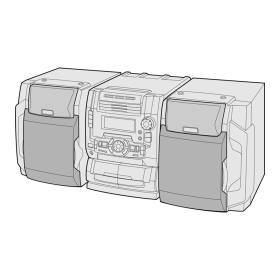
Page 4: Names Of Parts
CD-C1W,CP-C1W NAMES OF PARTS CD-C1W 1 2 3 4 5 6 Front panel Disc 1 Select/Direct Play Button Disc 1 Open/Close Button Disc 2 Select/Direct Play Button Disc 2 Open/Close Button Disc 3 Select/Direct Play Button Disc 3 Open/Close Button... -
Page 5: 12. Line Output Sockets
CD-C1W,CP-C1W Rear panel Video/Auxiliary (Audio Signal) Input Sockets Line Output Sockets Span Selector Switch AC Power Lead AC Voltage Selector FM 75 Ohms Aerial Terminal Aerial Earth Terminal SW1/SW2/MW Aerial Terminal Speaker Terminals Remote control Remote Control Transmitter LED CD control section... -
Page 6: Operation Manual
CD-C1W,CP-C1W OPERATION MANUAL SETTING THE CLOCK Press the ON/STAND-BY button to enter the stand-by mode. In this example, the clock is set for the 24-hour (0:00) system. Press the CLOCK button. Within 5 seconds, press the MEMORY/SET button. Turn the jog dial to select the time display mode. - Page 7 CD-C1W,CP-C1W – 7 –...
-
Page 8: Disassembly
CD-C1W,CP-C1W DISASSEMBLY CP-C1W Caution on Disassembly Follow the below-mentioned notes when disassembling PROCEDURE STEP REMOVAL FIGURE the unit and reassembling it, to keep it safe and ensure Front Panel 1. Net ......(A1) x1 10-2 excellent performance: 2. Net Holder ....(A2) x4 1. - Page 9 CD-C1W,CP-C1W (E5)x1 Ø3x8mm (N1)x2 (E4)x1 Ø3x10mm ø3x10mm (E3)x2 Display PWB (F1)x1 Power CD Changer Block Front Panel (E1)x1 Main PWB Pull (E1)x2 (E4)x1 (D2)x1 Ø3x10mm Ø3x10mm (E2)x1 Rear Panel (E5)x1 Ø3x8mm Tuner CD Servo PWB (F1)x1 CD Changer Holder Lug Wire...
- Page 10 CD-C1W,CP-C1W (R3) x1 Push (R1) x2 (R5) x1 ø2 x7mm ø2.6 x12mm Pawl (R6) x1 (R9) x1 Spring (R7) x2 ø2 x6mm Mechanism (R2) x1 Push the pawl of disc tray (R10) x4 with a proper screwdriver. (R8) x1 ø2.6 x10mm...
-
Page 11: Removing And Reinstalling The Main Parts
CD-C1W,CP-C1W REMOVING AND REINSTALLING THE MAIN PARTS CD MECHANISM SECTION (A1) x2 ø2.6 x5mm For the procedure to remove the CD mechanism from the Stop Washer (A3) x1 main unit, refer to Disassembling Procedure, Steps 1~10, and Pickup 19. (p.8). -
Page 12: Adjustment
CD-C1W,CP-C1W ADJUSTMENT • Bias Frequency MECHANISM SECTION • Driving Force Check Instrument Adjusting Point Specified Value Connection Torque Meter Specified Value 98 ± 10 kHz — CNP102 Play: TW-2412 Tape 1: Over 80 g Tape 2: Over 80 g • Bias Current •... -
Page 13: Test Mode
CD-C1W,CP-C1W • Setting the Test Mode TUNER SECTION Keeping the PAUSE button and TUNER button pressed, turn fL: Low-range frequency on POWER. Then, the frequency is initially set in the memory fH: High-renge frequency as shown in Table. Call it with the PRESET button to use it for •... - Page 14 CD-C1W,CP-C1W TEST MODE • Setting the test mode Any one of test mode can be set by pressing several keys as follows. Hold down the EQ and CD buttons, and press the POWER switch. TEST: CD operation test • TEST mode Function —...
- Page 15 CD-C1W,CP-C1W EXPLANATION OF AUTOMATIC SOUND VALUE CORRECTION CONTROL 1. Outline The recent trend is toward rise of CD record level in the world, for example rock, dancing music, etc. In case of continuous high level playback G-EQ (graphic equalizer) and VOL (Volume) are controlled (lowered) automatically after a lapse of specific time (10 minutes) so as to get the easy-to-listen sound level.
-
Page 16: Notes On Schematic Diagram
CD-C1W,CP-C1W NOTES ON SCHEMATIC DIAGRAM • The indicated voltage in each section is the one measured by • Resistor: Digital Multimeter between such a section and the chassis To differentiate the units of resistors, such symbol as K and with no signal given. -
Page 17: Block Diagram
CD-C1W,CP-C1W PICKUP IN SW702A M702 SLED MOTOR M701 SPINDLE MOTOR LASER DRIVER M56748FP FOCUS/TRACKING/ SPIN/SLIDE DRIVER LA9241M SL– SERVO AMP. 20 17 27 26 16.934MHz XOUT LC78622K SERVO SIGNAL CAM SWITCH VVDD SWB101 CONTROL SWB102 LVDD SWB103 RVDD SWB104 OPTICAL... - Page 18 CD-C1W,CP-C1W FM BAND PASS FILTER SO301 ANTENNA BFT01 TERMINAL ICT01 FM IF FM IF TA7358AP TT01 CF302 AM IF AM IF FM FRONT END CF352 T351 FM IF IN IC303 LT01 LT02 VR351 LA1832 FM MUTE LEVEL FM IF DET./FM MPX./AM IF...
- Page 19 CD-C1W,CP-C1W VF1 (AC) FL 701 FL DIPLAY VF2 (AC) RX701 REMOTE CONTROL SENSOR Q702~Q711 IC701 IX0206AW TUNER SD DATA1 KEY MATRIX FL DRIVER & COM1 SW701~SW713 CONTROLLER SCK1 SW717~SW727 SW732~SW734 KEY IN SW739~SW744 TUNER MUTE SW702 JOG DIAL LED701~LED706 LED707~LED709...
- Page 20 CD-C1W,CP-C1W MAIN PWB-B TAPE2 PLAY TAPE1 PLAY R-CH SENS, R-CH SENS, D101 QT03 VRD02 RT19 D102 1 2 3 4 5 6 7 8 9 10 11 SW202 SPAN CNP202 SELECTOR TAPE2 PLAY 100/10 L-CH SENS, 3 2 1 1 2 3...
- Page 21 CD-C1W,CP-C1W TAPE1 PLAY L-CH BIAS R-CH REC/PLAYSENS, L-CH BIAS R-CH SENS, CURRENT CURRENT Q148 Q114 VR152 Q154 VRD02 FW903 Q122 Q104 1 2 3 Q106 C152 1 2 3 3 2 1 R174 3 2 1 R156 CFW903 P38 6-C...
- Page 22 CD-C1W,CP-C1W GND(CD2) GND(CD1) CNP201 GND(D) RESET +7.3V(CD) GND(D) +12V(M) GND(D) +4.6V(D) +4.6V(D) +4.6V(µ-CON +12V(M) GND(µ-CON +12V(M) DATA1 C208 COM1 0.022 SCK1 R211 STB1 D206 R205 1SS133 C207 22/25 R210 100/10 SW202 SPAN SELECTOR R596 CD MUTE 50/9 2.2K RA79 0.7V R595 2.2K...
- Page 23 CD-C1W,CP-C1W CD GND(D2) CD GND(D2) CD GND(D1) CD GND(D1) GND(D) GND(D) +7.3V(CD) +7.3V(CD) +12V(M) +12V(M) +4.6V(D) +4.6V(D) +4.6V(µ-CON) GND(µ-CON) +12V(A) –B –15V D203 GND(D3) RESET 1SS133 +4.6V H/P SW Q201 KRC102 M LINE-MUTE R233 R235 RESET 4.0V POINT 4.0V R232 4.0V...
- Page 24 CD-C1W,CP-C1W MAIN PWB-B(2/4) PLAYBACK SIGNAL CD09 RECORD SIGNAL CD15 1/50 10/16 5.0V RD03 CD01 1/50 5.0V ICD01 (1/2) 4.9V HA12134A RD01 CD17 DOLBY NR 5.0V 10/16 0.2V TAPE2 PLAY 1.3V L-CH SENS. 4.8V RD10 VRD03 LD01 22K(B) 6.8mH CD03 CD05...
- Page 25 CD-C1W,CP-C1W PB.MUTE PB_MUTE H:ON L:OFF DOLBY PLAY/REC CD15 D-PB/REC 10/16 DOLBY ON/OFF D-ON/OFF RD05 4.9V PRE L-CH ICD03 P.B MUTING CD17 RD38 BA3311L QD01 10/16 3.3K REC./P.B.EQUALIZER AMP. 2SC2878 A CD31 RD43 RD21 2.2/50 330K 0.7V CD37 RD27 10/16 REC L-CH...
- Page 26 CD-C1W,CP-C1W FWM1 –COM –COM TAPE1 PLAY PLAY SW PLAY SW PHM1 SWE1 +5V SENSOR +5V SENSOR RM23 SENSOR OUT SENSOR OUT +SOL +SOL SOL1 SOLENOID 0.4V 12.2V TAPE1 RM09 SWITCHING DM01 DRIVER QM08 1SS133 12.2V SWE2 QM01 KRC104 M DRIVER 11.4V...
- Page 27 CD-C1W,CP-C1W MAIN PWB-B(3/4) GND(M) PLAY SW T1_PLAY SENSOR OUT T1_RUN T1_CROM H:CrO L:NOR QM20 KRC104 M T1_SOL +SOL 12.2V HIGH_SP H:HIGHT L:NOR HIGH_SP +12V(M) QM21 MOTOR KRC104 M +MTR H:ON L:OFF 12.2V QM22 KRC104 M +SOL T2_SOL 12.0V 0.3V T2_PLAY...
- Page 28 CD-C1W,CP-C1W Q451 KRA107 M 1.6V R462 100K -8.3V Q452 KRC107 M -8.3V R461 100K C484 2.2/50 C483 2.2/50 R467 1.6V 47/25 C485 R477 –B -8.3V C487 IC452 47/25 BU4066BC ZD452 SRS MODE MTZJ8.2C SELECTOR Q463 KRC107 M R456 100K R455...
- Page 29 CD-C1W,CP-C1W P21 129-B TO MAIN PWB RD(R) WH(W) COLOR CNP202 TABLE BROWN ORANGE YELLOW GREEN BLUE VIOLET GRAY WHITE BLACK PINK TUNER PWB-D 1 2 3 4 5 6 7 8 9 10 11 CNP303 C383 R373 R372 C380 C301...
- Page 30 CD-C1W,CP-C1W FM SIGNAL MW/SW1/SW2 SIGNAL R310 VD302-B KV1236Z23F T304 C306 Q309 SW2 ANT R311 D305 2SC2878 B 10P (UJ) C303 R312 100K 1SS135 0.022 D309 C309 1SS135 330P TC302 C304 C308 (UJ) R314 TRACKING 0.022 3.3K 8.2P D306 C312 Q365 0.022...
- Page 31 CD-C1W,CP-C1W TUNER PWB-D Q365 KRC107 M C343 15P (CH) C342 R358 0.022 8.2K R363 TP 302 VR351 2.2K 10K(B) L353 FM MUTE C371 R361 LEVEL 1/50 3.3K MUTING R350 Q353 2.7K KTC3199 GR C367 C372 R362 L356 0.65V 1/50 1/50 3.3K...
- Page 32 CD-C1W,CP-C1W CD SWITCH DISPLAY PWB-A1 PWB-A2 FW701 SW726 TUNER SW727 SW725 SW724 SW734 (BAND) TAPE 1/2 VIDEO/AUX POWER ON/ STAND-BY C709 C711 SW739 DISC 3 OPEN/CLOSE SW732 SW733 CLEAR MEMORY/SET Q719 REMOTE LED701 Q717 Q718 R723 Q721 Q720 CONTROL SENSOR...
- Page 33 CD-C1W,CP-C1W CD MOTOR PWB-E M702 FW701 SLED MOTOR CNP3A BIM3 SWB101 CAM1 SW739 DISC 3 SW702A SWB102 CAM2 OPEN/CLOSE PICKUP IN SWB103 CAM3 M701 CNS3B CNS3A SPINDLE MOTOR LED701 SWB104 CAM4 SW740 DISC3 COLOR TABLE R766 BROWN DISC 2 MOB1...
- Page 34 CD-C1W,CP-C1W 47/10 LASER DRIVER 1.5V 4.0V 3.4V 1/50 0.01 KTA1266 GR CNS2A CNS2B R2 68K 4.7K R3 82K 4.7/25 FIN2 2.0V – – 2.0V – CNP1 FIN1 2.0V 2.0V FEBAL – – 2.0V – FOSTA – 2.0V TOSTA 0.1/50 2.0V DGND –...
- Page 35 CD-C1W,CP-C1W R57 1K R58 1K R59 1K R60 1K R61 1K R62 1K R63 1K SERVO/SIGNAL 4.7/25 0.01 CONTROL CD SIGNAL TEST1 DEFI EFLG 1.8V SUB-CODE µ-COM SBSY INTERFACE 0.047 XVSS 1.8V R51 3.3M LC78622K X-TAL VVSS 1.8V GENERATOR XOUT 4.0V...
- Page 36 CD-C1W,CP-C1W DISPLAY PWB-A1 64 63 62 59 58 57 56 55 54 53 52 51 50 49 48 47 LED707 F-PLAY 333GTH2 LED725 LED708 333GTH2 STOP 333GTH2 LED709 LED726 333GTH4 333GTH4 FW853 –38(VP) 80 79 78 77 76 75 74 73 72 71 7 -32.5V...
- Page 37 CD-C1W,CP-C1W FL DISPLAY FL701 25 24 23 22 21 20 19 18 17 51 50 49 48 47 45 44 43 42 41 40 39 38 37 36 35 34 33 32 31 30 29 28 27 16 15 14...
- Page 38 CD-C1W,CP-C1W Q999 E C B R996 CNS901 CNP901 FW904 D998 D907 C997 M901 C990 R998 WT902 FAN MOTOR ZD901 E C B Q998 C995 C986 C989 B C E Q997 R967 FW903 R969 E C B C985 Q905 TO MAIN PWB...
- Page 39 CD-C1W,CP-C1W FW853 WT853 FROM DISPLAY P32 6-G D850 D870 CNS851 C866 RL851 D851 TO MAIN PWB CNP851 P21 12-H BI851 C854 C858 D858 C856 ZD853 ZD851 T851 POWER TRANSFORMER ZD852 C855 R851 (267) BLUE BROWN AC POWER SUPPLY CORD (267)
- Page 40 CD-C1W,CP-C1W POWER AMP. PWB-C1 FM SIGNAL Q903 KTC3200 GR 3.8V R919 2.2K C917 C907 R909 0.022 2.2/50 IC901 (1/2) R939 (ML) L901 1.5K STK41713 0.29µH POWER AMP. (1/2W) C911 R921 R989 10 10 11 R991 10 (1/2W) D901 R923 55.3V 1SS133 26.4V...
- Page 41 CD-C1W,CP-C1W SO901 RL901 SPEAKER TERMINALS RELAY L-CH – C921 6 OHMS – (ML) R-CH C923 D999 (ML) 1SS133 R927 (1/2W) D912 1SS133 D911 C970 R976 1SS133 CNP901 R928 CNS901 47/25 (1/2W) ZD999 MTZJ6.2B M901 9.3V R971 8.8V FAN MOTOR C924...
-
Page 42: Waveforms Of Cd Circuit
CD-C1W,CP-C1W WAVEFORMS OF CD CIRCUIT STOP PLAY FOCUS SERCH 0.5ms 0.50 V 10.0 V IC1 20 F.E 0.5ms 10.0 V 0.5ms 5.0 V 0.50 V IC1 54 DRF 0.5ms 1.00 V NORMAL DISC 0.5ms TN0=01 1.00 V 20ms PLAY 1.00 V 0.5ms... -
Page 43: Trouble Shooting
CD-C1W,CP-C1W TROUBLESHOOTING When the CD does not function When the CD section does not operate When the objective lens of the optical pickup is dirty,this section may not operate.Clean the objective lens,and check the playback operation.When this section does not operate even after the above step is taken,check the following items. - Page 44 CD-C1W,CP-C1W • The CD operation keys work. Check the FOCUS-HF system. Playback can be performed without a disc. Focus search OK Does the pickup move up and down two twice? Check the area around IC3 to CNP2. Does the output waveform of IC1 pin 16 (FD) match that...
- Page 45 CD-C1W,CP-C1W • Check the tracking system. Check the waveform of IC1 pin 7 (TE). The waveform shown in Figure 45-1 Check the periphery of IC1 pin 8 to Tracking servo is inoperative. appears, and no disc state appears pin 15, and IC5 to CNP2.
-
Page 46: Function Table Of Ic
CD-C1W,CP-C1W FUNCTION TABLE OF IC IC1 VHiLA9241M/-1:Servo Amp., (LA9241M) (1/2) Function Port Name Pin No. FIN2 Connection pin for photodiode of pickup. RF signal is generated through addition with FIN pin, and FE signal is generated through subtraction. FIN1 Connection pin for photodiode of pickup. - Page 47 CD-C1W,CP-C1W IC1 VHiLA9241M/-1:Servo Amp., (LA9241M) (2/2) Function Port Name Pin No. Micro computer command clock input pin. Micro computer command data input pin. Micro computer command chip enable input pin. (DETECT RF) RF level detection output. (Focus Serch Select) Pin to switch focus search mode. (± search/+ search for reference voltage) VCC2 VCC pin for servo system and digital system.
- Page 48 CD-C1W,CP-C1W IC2 VHiLC78623K-1:Servo/Signal Control(LC78623K) (1/2) Terminal Name Input/Output Function Pin No. DEFI Input Input terminal of defect detection signal (DEF). (Connected to OV when not used.) Input For PLL Input terminal for test. Pull-down resistor is integrated. Surely connected to 0V.
- Page 49 CD-C1W,CP-C1W IC2 VHiLC78623K-1:Servo/Signal Control(LC78623K) (2/2) Terminal Name Input/Output Pin No. Function Output Output terminal of subcodes P, A, R, S, T, U and W. SFSY Output Output terminal of synchronous signal of subcode frame. It drops when subcode stands by.
- Page 50 CD-C1W,CP-C1W IC201 RH-iX0210AWZZ: System Microcomputer (IX0210AW)(1/2) Function Pin No. Port Name Terminal Name Input/Output TRY SW3 Input TRY SW4 Input COIN Output CD command SQ_OUT Input CD Q code data SCK0 CQ CK Output CD seria clock Output DISP microcomputer control line...
- Page 51 CD-C1W,CP-C1W IC201 RH-iX0207AWZZ: System Microcomputer (IX0207AW) (2/2) Pin No. Port Name Terminal Name Input/Output Function SRS PASS Output SRS Specification SRS 3D/MONO Output SRS Specification SRS A Output SRS Specification SRS B Output SRS Specification SRS INH Output SRS Specification...
- Page 52 CD-C1W,CP-C1W IC501 VHiLC75396N-1:Audio Processor (LC75396N 201) Function Terminal Name Pin No. RF1C1-RF1C3 Terminal to connect capacitor of filter configuration for equalizer F1 band Connect the capacitor between LF1C1(RF1C1) and LF1C2(RF1C2) between LF1C2 (RF1C2) and LF1C3(RF1C3). RF2C1-RF2C3 Terminal to connect capacitor of filter configuration for equalizer F2 band Connect the capacitor between LF2C1(RF2C1) and LF2C2(RF2C2) between LF2C2 (RF2C2) and LF2C3(RF2C3).
- Page 53 CD-C1W,CP-C1W IC701 RH-iX0206AWZZ: FL Driver & Controller (IX0206AW) (1/2) Pin No. Port Name Function Terminal Name Input/Output P16/BUZZ DIP_STB Input Serial strobe input for system microcomputer P17/PWM0 Output LED17 Output LED output H: Lights R-play LED18 Output LED output H: Lights PAUSE...
- Page 54 CD-C1W,CP-C1W IC701 RH-iX0206AWZZ: FL Driver & Controller (IX0206AW) (2/2) Pin No. Port Name Function Terminal Name Input/Output S20/PC4 Output Display tube segment drive S21/PC5 Output Display tube segment drive S22/PC6 Output Display tube segment drive S23/PC7 Output Display tube segment drive...
-
Page 55: Fl Segment
CD-C1W,CP-C1W FL701 VVKCK1627M/-1 G1~G8 S6 S5 ONCE MEMORY RANDOM PLAY SLEEP X-BASS PIN ASSIGNMENT Pin No. 4 5 6 7 8 9 10 11 12 13 14 15 16 17 18 19 20 21 22 23 24 25 26 27 28 29 30 31 32... - Page 56 CD-C1W,CP-C1W –– MEMO–– – 56 –...
-
Page 57: Parts Guide
“HOW TO ORDER REPLACEMENT PARTS” To have your order filled promptly and correctly, please furnish the For U.S.A. only following information. Contact your nearest SHARP Parts Distributor to order. 1. MODEL NUMBER 2. REF. No. 3. PART NO. 4. DESCRIPTION For location of SHARP Parts Distributor, Please call Toll-Free;... - Page 58 CD-C1W, CP-C1W PRICE PRICE DESCRIPTION PART CODE PARTS CODE DESCRIPTION RANK RANK Q905,906 VSKTC3199GR-1 AB Silicon,NPN,KTC3199 GR CD-C1W Q994 VSKTA1270Y/-1 AD Silicon,PNP,KTA1270 Y Q995 VSKTC3199GR-1 AB Silicon,NPN,KTC3199 GR INTEGRATED CIRCUITS Q997~999 VSKTC3199GR-1 AB Silicon,NPN,KTC3199 GR QD01,02 VS2SC2878A/-1 AE Silicon,NPN,2SC2878 A...
- Page 59 CD-C1W, CP-C1W PRICE PRICE DESCRIPTION PARTS CODE DESCRIPTION PART CODE RANK RANK CAPACITORS ZD854 VHEMTZJ4R7B-1 AB Zener,4.7V,MTZJ4.7B ZD901 VHEMTZJ150A-1 AA Zener,15V,MTZJ15A AB 47 µF,10V,Electrolytic ZD903,904 VHEMTZJ8R2C-1 AB Zener,8.2V,MTZJ8.2C RC-GZA476AF1A AA 0.01 µF,16V ZD998 VHEMTZJ5R1B-1 AC Zener,5.1V,MTZJ5.1B VCTYMN1CY103K J AB 1 µF,50V,Electrolytic...
- Page 60 CD-C1W, CP-C1W PRICE PRICE PART CODE DESCRIPTION PARTS CODE DESCRIPTION RANK RANK AA 0.0082 µF,25V AB 2.2 µF,50V,Electrolytic C179,180 VCTYPA1EX822K C501~508 RC-GZA225AF1H AB 0.1 µF,50V,Electrolytic AB 10 µF,50V,Electrolytic C181,182 RC-GZA104AF1H C509,510 RC-GZA106AF1H AC 470 µF,10V,Electrolytic C201 RC-GZA477AF1A C511,512 VCKYMN1HB101K J AA 100 pF,50V AA 0.01 µF,16V...
- Page 61 CD-C1W, CP-C1W PRICE PRICE PART CODE DESCRIPTION PARTS CODE DESCRIPTION RANK RANK AB 1 µF,50V,Electrolytic CD9~11 RC-GZA105AF1H VRD-MN2BD223J AA 22 kohms,1/8W AA 0.22 µF,50V,Electrolytic CD12,13 RC-GZA224AF1H R35,36 VRD-MN2BD224J AA 220 kohms,1/8W AB 10 µF,16V,Electrolytic CD14~18 RC-GZA106AF1C VRD-ST2CD823J AA 82 kohms,1/6W...
- Page 62 CD-C1W, CP-C1W PRICE PRICE PART CODE DESCRIPTION PARTS CODE DESCRIPTION RANK RANK R195 VRD-MN2BD121J AA 120 ohms,1/8W R396~398 VRD-MN2BD102J AA 1 kohm,1/8W R196 VRD-ST2CD121J AA 120 ohms,1/6W R455 VRD-ST2CD104J AA 100 kohm,1/6W R197,198 VRD-MN2BD272J AA 2.7 kohms,1/8W R456 VRD-MN2BD104J AA 100 kohm,1/8W...
- Page 63 CD-C1W, CP-C1W PRICE PRICE PART CODE DESCRIPTION PARTS CODE DESCRIPTION RANK RANK R726 VRD-ST2CD102J AA 1 kohm,1/6W RA01 VRD-ST2CD102J AA 1 kohm,1/6W R727 VRD-ST2CD122J AA 1.2 kohms,1/6W RA02~05 VRD-MN2BD102J AA 1 kohm,1/8W R728 VRS-TV2AB182J AA 1.8 kohms,1/10W RA06~10 VRD-ST2CD102J AA 1 kohm,1/6W...
- Page 64 CD-C1W, CP-C1W PRICE PRICE DESCRIPTION PART CODE PARTS CODE DESCRIPTION RANK RANK RM09 VRD-MN2BD103J AA 10 kohm,1/8W F853 92LFUSE-T202E AD Fuse,T2A L 250V RM10 VRD-ST2CD103J AA 10 kohm,1/6W F854 92LFUSE-T502-E AD Fuse,T5A L 250V RM11,12 VRD-ST2CD222J AA 2.2 kohms,1/6W F855,856 92LFUSE-T252-E AD Fuse,T2.5A L 250V...
- Page 65 CD-C1W, CP-C1W PRICE PRICE PART CODE DESCRIPTION PARTS CODE DESCRIPTION RANK RANK SWB108 QSW-P0920AFZZ AC Switch,Push Type [CD Set] XEBSD20P07000 AB Screw,ø2×7mm SWE1 ———— — Switch,Leaf Type [Tape 1 Play] XEBSD20P06000 AA Screw,ø2×6mm (Supplies at REF NO. PWB-G) XEBSD26P12000 AA Screw,ø2.6×12mm SWE2 ————...
-
Page 66: Tweeter
CD-C1W, CP-C1W PRICE PRICE DESCRIPTION PART CODE PARTS CODE DESCRIPTION RANK RANK QCNWN1102AWZZ J AE Lead Wire with Lug TMAPC0093AWZZ J AC Schematic Diagram A TCAUS0014AWZZ J AC Label,Caution [Taiwan Only] [Australia/Thailand Only] TLABB0001AWZZ AB Label,Japan [Brazil Only] TMAPC0094AWZZ J... - Page 67 CD-C1W,CP-C1W CD-C1W 306-2 306-1 306-3 703x2 M701 M702 305x2 SW702A PWB-E Figure 10 CD MECHANISM EXPLODED VIEW – 10 –...
- Page 68 CD-C1W,CP-C1W CD-C1W CD Mechanism 805x4 803x2 804x3 104 105 801x2 111x2 110x2 108x3 108x3 SWB101 PWB-F ~104 MOB1 108x3 123x4 MOB2 80mm Figure 11 CHANGER MECHANISM EXPLODED VIEWCD-CIW – 11 –...
- Page 69 CD-C1W,CP-C1W CD-C1W 612x2 606x3 611x3 609x2 PWB-A2 CD Changer Block 612x2 606x12 PWB-C3 SW701 609x3 FL701 (Taiwan Only) (Brazil Only) SW702 614x2 (Taiwan Only) PWB-A1 611x12 606x2 611x2 201-3 PWB-B Q824 Silicon 609x3 Q822 Grease 603x2 Q820 201-1 PWB-A3 266x2...
- Page 70 CD-C1W,CP-C1W CP-C1W SUPER TWEETER SP5(L-CH) SP6(R-CH) TWEETER SP3(L-CH) 2.7µ,100V, SP4(R-CH) Film Capacitor SPERKER WOOFER TERMINAL SP1(L-CH) (910) SP2(R-CH) 919x2 918x2 SP3(L-CH) SP4(R-CH) 919x2 919x2 SP5(L-CH) SP6(R-CH) 916x4 TWEETER 916x2 SP3(L-CH) 906x4 SP4(R-CH) SUPER 920x4 TWEETER 917x4 SP1(L-CH) SP5(L-CH) SP2(R-CH) SP6(R-CH)
- Page 71 CD-C1W,CP-C1W –– MEMO –– – 14 –...
- Page 72 CD-C1W,CP-C1W © COPYRIGHT 1997 BY SHARP COPORATION ALL RIGHTS RESERVED. No part of this publication may be reproduced, stored in a retrieval system, or transmitted in any from or by any means, electronic, mechanical, photocopying, recording, or otherwise, without prior written permission of the publisher.
Need help?
Do you have a question about the CD-C1W and is the answer not in the manual?
Questions and answers