Table of Contents
Advertisement
16-BIT HMOS MICROPROCESSOR
Direct Addressing Capability 1 MByte
Y
of Memory
Architecture Designed for Powerful
Y
Assembly Language and Efficient High
Level Languages
14 Word by 16-Bit Register Set with
Y
Symmetrical Operations
24 Operand Addressing Modes
Y
Bit Byte Word and Block Operations
Y
8 and 16-Bit Signed and Unsigned
Y
Arithmetic in Binary or Decimal
Including Multiply and Divide
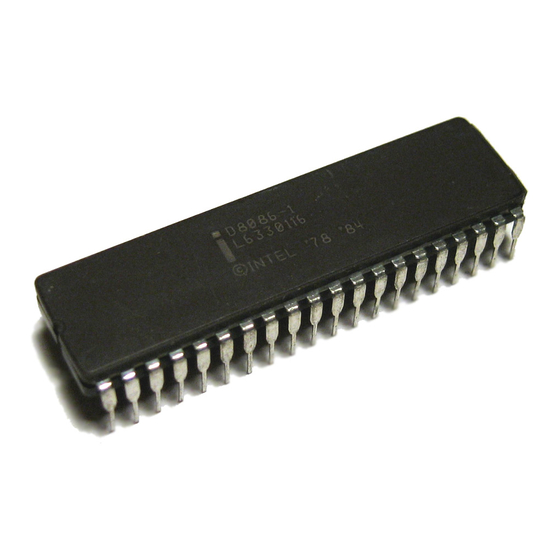
The Intel 8086 high performance 16-bit CPU is available in three clock rates 5 8 and 10 MHz The CPU is
implemented in N-Channel depletion load silicon gate technology (HMOS-III) and packaged in a 40-pin
CERDIP or plastic package The 8086 operates in both single processor and multiple processor configurations
to achieve high performance levels
Figure 1 8086 CPU Block Diagram
September 1990
8086
8086 8086-2 8086-1
Range of Clock Rates
Y
5 MHz for 8086
8 MHz for 8086-2
10 MHz for 8086-1
MULTIBUS System Compatible
Y
Interface
Available in EXPRESS
Y
Available in 40-Lead Cerdip and Plastic
Y
Package
(See Packaging Spec Order
231455 –1
Standard Temperature Range
Extended Temperature Range
231369)
40 Lead
Figure 2 8086 Pin
Configuration
Order Number 231455-005
231455 – 2
Advertisement
Table of Contents

Related Manuals for Intel 8086


Summary of Contents for Intel 8086
- Page 1 Arithmetic in Binary or Decimal Including Multiply and Divide The Intel 8086 high performance 16-bit CPU is available in three clock rates 5 8 and 10 MHz The CPU is implemented in N-Channel depletion load silicon gate technology (HMOS-III) and packaged in a 40-pin...
- Page 2 8086 The following pin function descriptions are for 8086 systems in either minimum or maximum mode The ‘‘Local Bus’’ in these descriptions is the direct multiplexed bus interface connection to the 8086 (without regard to additional bus buffers) Symbol Pin No Type –AD...
- Page 3 The two modes are discussed in the following sections The following pin function descriptions are for the 8086 8288 system in maximum mode (i e MN MX Only the pin functions which are unique to maximum mode are described all other pin functions are as described above 26–...
- Page 4 ‘‘hold acknowledge’’ 3 A pulse 1 CLK wide from the requesting master indicates to the 8086 (pulse 3) that the ‘‘hold’’ request is about to end and that the 8086 can reclaim the local bus at the next CLK...
- Page 5 8086 instruction queue 0 (LOW) 1 (HIGH) The following pin function descriptions are for the 8086 in minimum mode (i e MN MX functions which are unique to minimum mode are described all other pin functions are as described above M IO...
-
Page 6: Functional Description
8086 FUNCTIONAL DESCRIPTION General Operation The internal functions of the 8086 processor are partitioned logically into two processing units The first is the Bus Interface Unit (BIU) and the second is the Execution Unit (EU) as shown in the block dia-... -
Page 7: Bus Operation
231455–3 pins changes dependent on the condition of the strap pin When MN MX pin is strapped to GND the 8086 treats pins 24 through 31 in maximum mode An 8288 bus controller interprets status information coded into S control signals compatible with the MULTIBUS ar-... - Page 8 8086 Figure 4a Minimum Mode 8086 Typical Configuration Figure 4b Maximum Mode 8086 Typical Configuration 231455 – 5 231455 – 6...
- Page 9 8086 bus cycles These are re- ferred to as ‘‘Idle’’ states (T ) or inactive CLK cycles The processor uses these cycles for internal house- keeping During T of any bus cycle the ALE (Address Latch Enable) signal is emitted (by either the processor or...
-
Page 10: Interrupt Operations
I O ADDRESSING In the 8086 I O operations can address up to a maximum of 64K I O byte registers or 32K I O word registers The I O address appears in the same for-... - Page 11 ‘‘HALT’’ state when a local bus ‘‘hold’’ is entered while in ‘‘HALT’’ In this case the proces- sor reissues the HALT indicator An interrupt request or RESET will force the 8086 out of the ‘‘HALT’’ state READ MODIFY WRITE (SEMAPHORE)
- Page 12 This activity does not consume bus cycles The processor remains in an idle state while waiting All 8086 drivers go to 3-state OFF if bus ‘‘Hold’’ is en- tered If interrupts are enabled they may occur while the processor is waiting When this occurs the proc-...
- Page 13 8086 is capable of handling Signals ALE DEN and DT R are generated by the...
-
Page 14: Absolute Maximum Ratings
(8086-2 T Symbol Parameter Input Low Voltage Input High Voltage Output Low Voltage Output High Voltage Power Supply Current 8086 8086-1 8086-2 Input Leakage Current Output Leakage Current Clock Input Low Voltage Clock Input High Voltage Capacitance of Input Buffer (All input except –... - Page 15 8284A (See Notes 1 2) TCLR1X RDY Hold Time into 8284A (See Notes 1 2) TRYHCH READY Setup Time into 8086 TCHRYX READY Hold Time into 8086 TRYLCL READY Inactive to CLK (See Note 3) THVCH HOLD Setup Time...
- Page 16 TCLCH-10 TCLCH-10 TCHCL-10 TCHCL-10 TCLCH-25 TCLCH-30 TCLCL-35 TCLCL-40 2TCLCL-40 2TCLCL-50 2TCLCL-35 2TCLCL-40 TCLCH-35 TCLCH-40 Test Units Conditions 20–100 pF for all 8086 Outputs (In addition to 8086 selfload) From 0 8V to 2 0V From 2 0V to 0 8V...
-
Page 17: Minimum Mode
A C Testing Inputs are driven at 2 4V for a Logic ‘‘1’’ and 0 45V for a Logic ‘‘0’’ Timing measurements are made at 1 5V for both a Logic ‘‘1’’ and ‘‘0’’ WAVEFORMS MINIMUM MODE A C TESTING LOAD CIRCUIT 231455-11 Includes Jig Capacitance 8086 231455 –12 231455 –13... - Page 18 V 2 RDY is sampled near the end of T 3 Two INTA cycles run back-to-back The 8086 LOCAL ADDR DATA BUS is floating during both INTA cycles Control signals shown for second INTA cycle 4 Signals at 8284A are shown for reference only...
- Page 19 RDY Setup Time into 8284A (Notes 1 2) TCLR1X RDY Hold Time into 8284A (Notes 1 2) TRYHCH READY Setup Time into 8086 TCHRYX READY Hold Time into 8086 TRYLCL READY Inactive to CLK (Note 4) TINVCH Setup Time for...
- Page 20 Control Inactive Delay (See Note 1) TAZRL Address Float to READ Active TCLRL RD Active Delay TCLRH RD Inactive Delay 8086 8086-1 8086-2 TCLAX Test Units Conditions 20 – 100 pF for all 8086 Outputs (In addition to 8086 self-load)
- Page 21 4 Applies only to T2 state (8 ns into T3) 8086-1 8086-2 TCLCL-35 TCLCL-40 2TCLCL-40 2TCLCL-50 8086 Test Units Conditions 20 – 100 pF for all 8086 Outputs (In addition to 8086 self-load) From 0 8V to 2 0V From 2 0V to 0 8V...
-
Page 22: Maximum Mode
8086 WAVEFORMS MAXIMUM MODE 231455 –15... - Page 23 2 RDY is sampled near the end of T 3 Cascade address is valid between first and second INTA cycle 4 Two INTA cycles run back-to-back The 8086 LOCAL ADDR DATA BUS is floating during both INTA cycles Control for pointer address is shown for second INTA cycle...
-
Page 24: Reset Timing
8086 WAVEFORMS (Continued) ASYNCHRONOUS SIGNAL RECOGNITION NOTE 1 Setup requirements for asynchronous signals only to guarantee recognition at next CLK BUS LOCK SIGNAL TIMING (MAXIMUM MODE ONLY) REQUEST GRANT SEQUENCE TIMING (MAXIMUM MODE ONLY) NOTE The coprocessor may not drive the buses outside the region shown without risking contention RESET TIMING 231455–... - Page 25 8086 WAVEFORMS (Continued) HOLD HOLD ACKNOWLEDGE TIMING (MINIMUM MODE ONLY) 231455 –21...
-
Page 26: Data Transfer
8086 Table 2 Instruction Set Summary Mnemonic and Description DATA TRANSFER Move Register Memory to from Register Immediate to Register Memory Immediate to Register Memory to Accumulator Accumulator to Memory Register Memory to Segment Register Segment Register to Register Memory... - Page 27 ASCII Adjust for Divide Convert Byte to Word Convert Word to Double Word Mnemonics Intel 1978 Instruction Code 7 6 5 4 3 2 1 0 7 6 5 4 3 2 1 0 7 6 5 4 3 2 1 0...
-
Page 28: Control Transfer
8086 Table 2 Instruction Set Summary (Continued) Mnemonic and Description LOGIC Invert SHL SAL Shift Logical Arithmetic Left Shift Logical Right Shift Arithmetic Right Rotate Left Rotate Right Rotate Through Carry Flag Left Rotate Through Carry Right Reg Memory and Register to Either... - Page 29 1 1 1 0 0 0 1 1 disp 1 1 0 0 1 1 0 1 type 1 1 0 0 1 1 0 0 1 1 0 0 1 1 1 0 1 1 0 0 1 1 1 1 8086...
-
Page 30: Processor Control
The following list represents key differences between this and the -004 data sheet Please review this summa- ry carefully 1 The Intel 8086 implementation technology (HMOS) has been changed to (HMOS-III) 2 Delete all ‘‘changes from 1985 Handbook Specification’’ sentences...