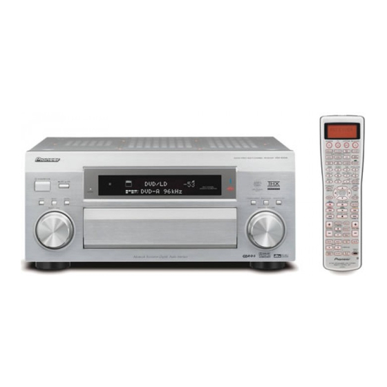
Pioneer VSX-AX5Ai-S Service Manual
Audio/video multi-channel receiver
Hide thumbs
Also See for VSX-AX5Ai-S:
- Operating instructions manual (108 pages) ,
- Operating instructions manual (30 pages)
Table of Contents
Advertisement
Quick Links
sound. vision.souI
S ervice
Manual
OR DE R N O .
RR V3 01 8
VSX -AX 5Ai - S
A U DIO /VID E O M U L T I- C H A N N E L R E C E IV E R
VSX-AX5Ai-
S
TH IS M AN UA L IS A PP LI CA BL E T O TH E FO LL OW ING MOD EL (S ) A N D TY PE (S ).
Th e voltag e ca n b e converte d b y th e
Mode l
Powe r Requiremen
t
Ty p e
fol low in g m eth od .
VS X-A X5A i-S
HY X J
AC 220 -23 0 V
AC 240 V , *
*: A lter the wir in g of the power-s uppl y bloc k at the prima r y win din g of P ower tra ns forme r referrin g to the L ine Voltag e S elec tio n
des c ribe d in S ervic e Manual.
T-ZZ V AU G . 20 0 4 pri nted i n Ja pa n
Advertisement
Table of Contents

Related Manuals for Pioneer VSX-AX5Ai-S


Summary of Contents for Pioneer VSX-AX5Ai-S
- Page 1 sound. vision.souI S ervice Manual OR DE R N O . RR V3 01 8 VSX -AX 5Ai - S A U DIO /VID E O M U L T I- C H A N N E L R E C E IV E R VSX-AX5Ai- TH IS M AN UA L IS A PP LI CA BL E T O TH E FO LL OW ING MOD EL (S ) A N D TY PE (S ).
-
Page 2: Safty Information
PIONEER Service Manual. A subscription to, or additional copies Also test with plug reversed of, PIONEER Ser vice Manual may be obtained at a (Using AC adapter Earth nominal charge from PIONEER. plug as required) - Page 3 To protect products from damages or failures during transit, the shipping mode should be set or the shipping screws should be installed before shipment. Please be sure to follow this method especially if it is specified in this manual. VSX-AX5Ai-S...
-
Page 4: Table Of Contents
4.20 SP/PS ASSY ............................112 4.21 DIODE, TRANS 2-1 and VH TR ASSYS ....................114 4.22 TRANS 2-2, TRANS 1 and PRIMARY ASSYS..................116 4.23 VIDEO CONVERT ASSY ........................118 5. PCB PARTS LIST ............................119 6. ADJUSTMENT ............................. 129 VSX-AX5Ai-S... - Page 5 7.1.2 DIAGNOSTICS OF AMPLIFIER SECTION..................132 7.1.3 TROUBLE SHOOTING........................133 7.1.4 OUTLINE OF THE 1394 UNIT ......................138 7.1.5 DISASSEMBLY ..........................140 7.2 PARTS ..............................145 7.2.1 IC..............................145 7.2.2 DISPLAY ............................171 7.3 CLEANING .............................173 7.4 REMOTE CONTROL UNIT........................174 7.4.1 EXPLODED VIEWS AND PARTS LIST....................174 8. PANEL FACILITIES ............................175 VSX-AX5Ai-S...
-
Page 6: Specifications
THX and Dolby Laboratories, and is a trademark of Dolby Laboratories. All rights reserved. Used under authorization. • Manufactured under license from Dolby Laboratories. “Dolby”, “Pro Logic”, “Surround EX” and double-D symbol are trademarks of Dolby Laboratories. • "DTS", "DTS-ES Extended Surround" and "Neo:6" are trademarks of Digital Theater Systems, Inc. VSX-AX5Ai-S... - Page 7 Accessories AM Loop Antenna FM Wire Antenna (ATB7013) (ADH7030) AC Power Cord (ADG7062) "AA" IEC LR6 batteries Microphone for Auto Microphone Stand for Auto Surround Sound Setup Surround Sound Setup Remote Control Unit (APM7004) (AEB7269) (AXD7364) VSX-AX5Ai-S...
-
Page 8: Exploded Views And Parts List
For the applying amount of lubricants or glue, follow the instructions in this manual. (In the case of no amount instructions, apply as you think it appropriate.) 2.1 PACKING 9 to 14 (Operating Instructions) VSX-AX5Ai-S... - Page 9 Operating Instructions ARC7544 (French / Spanish) Operating Instructions ARC7545 (Dutch) Caution Sheet SP, E ARM7056 NSP 16 Warranty Card ARY7065 NSP 17 Polyethylene Bag AHG7117 Packing Sheet RHC1023 Front Pad 45 AHA7374 Rear Pad 45 AHA7375 Packing Case AX5A/HY AHD8273 VSX-AX5Ai-S...
-
Page 10: Exterior Section
2.2 EXTERIOR SECTION 19 19 (×6) (×10) (×2) (×2) Refer to "2.3 CHASSIS SECTION". Refer to "2.6 FRONT PANEL SECTION". VSX-AX5Ai-S... - Page 11 Bonnet Sheet (2 x 50 x 50) AEB7329 • • • • • NSP 15 Binder ZCA-BK1 • • • • • • • • • • Label (DD/DTS/THX) ARW7281 Screw ABA7098 Screw ABA7119 Screw ABA7102 Screw ABA7118 Screw ABA7101 Screw ABA7120 Screw ABA7110 VSX-AX5Ai-S...
-
Page 12: Chassis Section
2.3 CHASSIS SECTION Refer to "2.5 HEATSINK SECTION". 37 48 Refer to "2.4 REAR PANEL SECTION". VSX-AX5Ai-S... - Page 13 • • • • • NSP 40 Tape ZTA-156A-19 Cushion 11 x 11 AED7088 > Fan Motor (Rear) AXM7031 Fan Plate ANG7153 NSP 44 Mini Clamp VEC1597 • • • • • Screw ABA7098 Screw ABA7109 Screw ABA7102 Screw ABA7101 VSX-AX5Ai-S...
-
Page 14: Rear Panel Section
2.4 REAR PANEL SECTION REGULATOR CN2403 REGULATOR CN2404 REGULATOR CN2405 CN601 POWER AMP IN CN4001 CN701 CN2415 DSP CONNECTION CN702 DISPLAY CN101 CN3006 CN2413 CN2411 CN2410 REGULATOR CN2414 CN2412 VSX-AX5Ai-S... - Page 15 • • • • • Speaker Sheet KU AAK8016 Cushion Circle 16B AED7052 Rear Panel AX5AI ANC8280 Cushion Circle 6B AED7044 NSP 25 Tape PNM1249 Terminal Screw AKE-031 Screw ABA7098 Screw ABA7102 Screw ABA1208 Screw ABA7078 Screw PCZ26P060FCC Screw PMZ30P060FCC VSX-AX5Ai-S...
-
Page 16: Heat Sink Section
2.5 HEAT SINK SECTION MAIN CONTROL CN801 VSX-AX5Ai-S... - Page 17 Fan Motor (Front) AXM7032 Mica Sheet 45 AEE7047 H.S Angle 45 ANG7404 PCB Angle 45 ANG7406 Fan Holder 80 ANG7407 NSP 12 Heatsink 45 ANH7152 NSP 13 Speed Clamp AEC7445 NSP 14 Wire Saddle DEC1450 Screw ABA7102 Screw ABA7085 Screw BBZ30P300FTC VSX-AX5Ai-S...
-
Page 18: Front Panel Section
2.6 FRONT PANEL SECTION PRIMARY CN2002 25 (2/2) MAIN CONTROL CN501 25 (1/2) No. 25 (2/2) Magnet Holder VSX-AX5Ai-S... - Page 19 AMF7007 Door Shaft 35 AMR7295 F. Panel AX5A SHY ANB7349 Earth Plate A ANG7411 Earth Plate B ANG7412 Damper Assy (200) AXA7088 Pioneer Badge VAM1124 Holder VEC1355 NSP 34 Styling Assy • • • • • NK90FUC Screw ABA7098 Screw...
-
Page 20: Block Diagram And Schematic Diagram
(7P) (7P) CN1307 (9P) CN1301 IC1301 (1/2) FRONT IN DISPLAY UPC4570G2 3 ASSY ASSY FRONT CN1204 (1/2)(17P) SURROUND IC1302 (1/2) UPC4570G2 CN1302 IC1303 (1/2) CENTER UPC4570G2 IC1303 (2/2) SUB WOOFER UPC4570G2 SURROUND BACK IC1304 (1/2) UPC4570G2 V-AUDIO IN ASSY VSX-AX5Ai-S... - Page 21 MR Volume UPC4570G2 SW Amp. MR L MULTI-ROOM & SOURCE V1/OUT V1OL V2/OUT V2OL INPUT CONNECT ASSY CN1205 (3/3) CN1408 (9P) VCR1 CN1308 (9P) CN1201 7.1 CH I/O ASSY (2/2) CN1303 SUB WOOFER VCR2 CENTER FRONT CN1304 SURROUND SURROUND BACK VSX-AX5Ai-S...
-
Page 22: Dsp Block Diagram
3.1.2 DSP BLOCK DIAGRAM DSP ASSY IC101 CN301 AK5380VT IC201 CN1802 AK4114VQ DIR & DIT CN651 CN401 IC701 TC74VHC157FT SELECTOR IC302 IS61LV6416-12T SRAM IC301 DSPC56367PV150 DECODER IC303 DSP1 IS63LV1024-12T SRAM IC705 TC7SH04FU IC706 INVERTER TC7SH04FU IC305 TC7W125FU 3 STATE BUFFER INVERTER CN402 VSX-AX5Ai-S... - Page 23 IC501 AK4383VT IC521 AK4383VT IC503 TC7SH04FU BUFFER IC541 AK4383VT IC561 AK4382AVT IC401 DSPC56367PV150 DSP2 VSX-AX5Ai-S...
-
Page 24: 1394 Block Diagram
3.1.3 1394 BLOCK DIAGRAM 1394 ASSY VSX-AX5Ai-S... -
Page 25: Power Amp Block Diagram
3.1.4 POWER AMP BLOCK DIAGRAM VSX-AX5Ai-S... -
Page 26: Video Block Diagram
CN3201 MAIN CN2405 REGULATOR ASSY DISPLAY CONTROL ASSY ASSY CN3006 CN1501 CN3005 CN501 JA1501 FRONT FRONT IN VIDEO ASSY JA602 CN3202 JA3201(1/2) COMPOSITE IC3206 SELECT VCR2 JA3202(1/2) NJM2595M IC3207 VCR1 SELECT JA3203 NJM2595M DVD/LD IC3204 C/DC SELECT TV/SAT NJM2596M VSX-AX5Ai-S... - Page 27 1H DELAY B-Y2 VIDEO CONVERT R-Y2 ASSY TC74LVX4053FT TA1270BF TA8772AN CN3502 CN3203 VIDEO ASSY SELECT IC3202 IC3201 S:through IC3209(1/2) /V.C JA3204 TK15420M MONITOR IC3209(2/2) TK15420M TC74LVX4053FT TC74LVX4053FT JA3201(2/2) VCR2 IC3203 MULTI ROOM JA3205 MULTI SELECT ROOM JA3202(2/2) NJM2279M VCR2 VSX-AX5Ai-S...
-
Page 28: Overall Wiring Diagram
CN801 CN4402 ADX7404 ADD7355 CN601 CN4454 CN4453 J1902 CN701 CN702 CN101 J1902 ADE7085 CN1802 CN401 CN402 INPUT CONNECT ASSY (AWX8546) CN1405 CN1406 CN1407 CN1408 CN1204 CN1307 CN1306 CN1308 FM/AM TUNER UNIT (AXX7170) CN3203 CN3502 VIDEO CONVERT ASSY PF10PG-B10 (AWX8451) VSX-AX5Ai-S... - Page 29 0615E (AWX8551) ADX7399 J2201 2202 CN4702 ADX7286 DIODE ASSY (AWX8555) CN4456 CN4455 ADX7285 POWER AMP-C ASSY AXM7031 (AWX8562) ADX7397 4601 ADX7284 ADX7287 ADX7288 CN2002 PRIMARY ASSY CN1902 (AWX8461) REK-106 D20PYY0830E (T4A) 2007 AC IN CN4402 POWER CABLE CN3501 ADG7062 VSX-AX5Ai-S...
-
Page 30: I/O, V-Audio In, Front In And Optical In Assys
AMUTE (2/2) Q1372 R1378 R1380 (1/2) R1372 R1374 R1376 C1394 HN1C03F(AB) HN1C03F(AB) 0.01 (SB) R1381 R1383 R1385 HN1C03F(AB) HN1C03F(AB) (SB) R1387 R1389 Q1381 (1/2) SURROUND Q1382 BACK (2/2) Q1382 R1388 R1390 (1/2) R1382 R1384 R1386 CN1304 HN1C03F(AB) HN1C03F(AB) (2/2) VSX-AX5Ai-S... - Page 31 CN1501 JA1501 DOUT2 (2/4) 52044-0745 AKX7016 JA1703 FV-R GP1FA502TZ JA1501 (3/4) OUT1 AKX7016 FV-L VIDEO R1703 R1510 C1703 FV-C R1509 FV-Y JA1704 R1508 GP1FA502TZ OUT2 S-VIDEO R1704 F1701 C1704 DTF1064 JA1501 (4/4) AKX7016 KN1501 VNF1084 B C D CHASSIS VSX-AX5Ai-S...
-
Page 32: Input Connect And 12V Trigger Assys
CN1307 GNDA GNDA GNDA (SB) (SB) CN1407 XKP3062 GNDA V-15V GNDA GNDA V-15V CN1306 V+15V CN1404 CN1408 XKP3075 XKP3064 AMUTE AMUTE (SB) (SB) CN1308 IC1541 (1/2) C1451 UPC4570G2-A 10/50 C1452 10/50 IC1541 (2/2) C1453 4700p UPC4570G2-A R1453 SW. Amp. VSX-AX5Ai-S... - Page 33 : AUDIO SIGNAL ROUTE (MULTI-ROOM Lch) (DVD) : AUDIO SIGNAL ROUTE (DVD Lch) : AUDIO SIGNAL ROUTE (FRONT Lch) : AUDIO SIGNAL ROUTE (SURROUND Lch) (SB) : AUDIO SIGNAL ROUTE (SURROUND BACK Lch) : AUDIO SIGNAL ROUTE (CENTER ch) VSX-AX5Ai-S...
-
Page 34: Coaxial In Assy
IC1881 (2/6) C1884 IC1881 (4/6) 0.01 TC74HCU04AF TC74HCU04AF JA1802 R1884 (2/2) GNDD DSP+5V R1894 STBY R1898 GDCH R1899 OPT IN1 OPT IN2 GNDD OPT OUT1 A+15V OPT OUT2 DSP+5V CN1801 DSP+5V 52045-0945 A-15V (UD) GDA2 GNDD (UD) CN2406 CN101 VSX-AX5Ai-S... - Page 35 DGNDUSB DOUT BODY R1688 HID0 STBY C1689 HID1 Vccxi HID2 AGNDX C1688 ASS7047 GDCH SEL0 C1684 SEL1 C1687 R1689 Vccci Vccp2i AGND AGNDP 2.2k VinL Vccp1i GDCH C1698 VinR VoutL C1686 VoutR Vcom C1685 C1682 GNDD STBY (UD) (UD) VSX-AX5Ai-S...
-
Page 36: Component Assy
(PB) stby Q4414 (PR) V+5V (PR) V+5V Q4405 stby (2/3) C4427 (PB) Q4407 IN2 P stby R4442 (3/3) Q4408 (PR) Q4406 IC4405 OPA2652U (2/2) V-5V V-5V TP4433 TP4434 -MARKS TP4436 TP4444 TP4438 TP4440 TP4442 2SC4081(RS) 2SA1576A(RS) CN4403 52045-1245 VSX-AX5Ai-S... - Page 37 STROBE 10/16 EXDT SERIAL IN EXCK Q4410 Q4412 TP4451 CINH TP4450 DINH V-5V TP4449 V+5V BU4094BCF V-5V TP4401 TP4402 TP4403 TP4419 TP4404 TP4418 TP4405 TP4417 TP4416 TP4406 TP4415 TP4407 TP4414 TP4408 TP4413 TP4409 TP4412 TP4410 TP4411 CN4401 XKP3080 CN2404 VSX-AX5Ai-S...
-
Page 38: Video Assy
C3270 VIDEO 100/16 C3230 C / DC C3273 Selector 100/16 S-VIDEO (4/4) JA3203 V-5V R3271 R3281 R3280 D3202 R3282 DAN202K TP3212 MUTE TP3213 TP3214 +12V TP3221 TP3215 TP3220 V+5V TP3211 TP3216 TP3219 TP3210 TP3217 TP3218 TP3209 V-5V J602 CN2405 VSX-AX5Ai-S... - Page 39 R3286 MUTE MUTE MUTE VIDEO R3283 C3241 R3284 S-VIDEO : VIDEO SIGNAL ROUTE (MR) : VIDEO SIGNAL ROUTE (MULTI-ROOM) (4/4) (SY) : VIDEO SIGNAL ROUTE (S VIDEO Y ch) JA3202 (SC) : VIDEO SIGNAL ROUTE (S VIDEO C ch) VSX-AX5Ai-S...
-
Page 40: Main Control Assy (1/3)
C174 CD-R GNDU C172 R170 IC106 JA111 10/50 C175 (2/2) R123 4.7k 0.1/25 R172 C178 DMFL PHONO R173 C173 V-15 0.01 10/50 GNDA R124 IC106 UPC4570G2-A GNDU (1/2) R176 DMFR 4.7k UPC4570G2-A (2/2) GNDA CHASSIS JA111-JA113 ; VKB1133 CN1401 VSX-AX5Ai-S... - Page 41 (DVD) GNDA 2SK208(YGR) : AUDIO SIGNAL ROUTE (DVD Lch) GNDU V-15 6.8k CN1402 : AUDIO SIGNAL ROUTE (FRONT Lch) : AUDIO SIGNAL ROUTE (SURROUND Lch) (SB) : AUDIO SIGNAL ROUTE (SURROUND BACK Lch) : AUDIO SIGNAL ROUTE (CENTER ch) VSX-AX5Ai-S...
-
Page 42: Main Control Assy (2/3)
100p (SB) C773 (SB) C781 C786 10/50 (SB) GNDU 47/25 100p C787 IC714 R773 (SB) 100p (1/2) 100k UPC4570G2-A C777 47/25 GNDA IC704 TC94A07F C778 TP22 TP23 47/25 IC714 R774 UPC4570G2-A 100k (2/2) C782 C774 47/25 10/50 V-15 C780 VSX-AX5Ai-S... - Page 43 TP25 AMUTE AMUTE IC713 R754 UPC4570G2-A 100k (2/2) C762 C754 47/25 10/50 : AUDIO SIGNAL ROUTE (FRONT Lch) C760 : AUDIO SIGNAL ROUTE (SURROUND Lch) (SB) : AUDIO SIGNAL ROUTE (SURROUND BACK Lch) : AUDIO SIGNAL ROUTE (CENTER ch) VSX-AX5Ai-S...
-
Page 44: Main Control Assy (3/3)
0.01 GNDU C534 IC502 BU4094BCF R531 EXPST R534 stby R532 EXPDT EXPOE DATA R535 R533 EXPCK 2296SW5 R540 DEMSTP 2296SW4 R536 R541 2296SW3 DEMRST R537 R542 2296SW2 R538 Q'S' R539 GNDT V+12V C535 TP33 GNDA 0.01 CN2412 CN2415 CN2414 VSX-AX5Ai-S... - Page 45 DSP MODE2 16_3 D-MUTE R515 RXD232C MUTE GNDU DSDM R518 R519 R527 R528 U+5V 100k 100k GNDU CN552 DSDM 52045-1045 232CTXD T-RXD(31) 232CCTS T-BUSY(34) Buffer (T-Vpp) U+5V T-Vdd T-SCLK(33) 232CRXD T-TXD(32) CMVSS T-PGM(9) XRESET T-RST(12) TP34 GNDU GNDU CN2413 VSX-AX5Ai-S...
-
Page 46: Mic & F.opt In, Mic Amp And Dsp Connection Assys
MICOUT S3B-PH-K-S 10/50 CN1652 MICIN GNDA XKP3079 R4754 GNDA V-15 D1RT ADRT ADRT SHLD V+15 C4754 DATA R1674 DRDO DRDO DRCS DRCS DRRT IC4751 DRRT NJM78L05A IEIT IEDO IEDO IC4752 (2/2) IEDI IERT IECK IECS UPC4570G2-A K L M VSX-AX5Ai-S... - Page 47 R1664 Level Shift 5V -> 3.3V R1665 -15V -15V R1666 OPTIN DOUT V-15V ADRT ADRT DRCS DRCS V+3R3V DATA R1675 DRRT DRDO DRDO DRRT 1394IT R1676 IEDO 1394DO 1394DI R1662 1394RT 1394CK 1394CS R1677 STBY R1659 R1660 R1661 STBY VSX-AX5Ai-S...
-
Page 48: Power Amp In, Fan Connection And Fan Drive Assys
R4003 GNDSR Q4001 GNDSL R4004 GNDC GNDFR CN4004 F.FAN+ GNDFL D4001 V-15V F.FAN- DC DET F.FANSTOP OL DET AMUTE S3B-EH V+5.6V F.FAN+ TEMP LOFAN F.FAN- FAN STOP F.FANSTOP GNDU FAN DRV FAN STOP FANDRV LOFAN (SB) 4001 51048-1000 CN4401 VSX-AX5Ai-S... - Page 49 D4051 REG B 1SR154 REG G Q4052 D4052 DTA124EK R4053 REG B 1SR154 R4054 STBY CN4054 52147-1010 C4056 C4055 330/63 330/63 Q4053 R4052 Q4056 100k 2SA1037K Q4055 LOFAN DTC114EK DTC124EK D4055 UDZS12B FANDRV FAN STOP F.FANSTOP F.FAN- F.FAN+ D4059 VSX-AX5Ai-S...
-
Page 50: Dsp Assy (1/2)
(6/6) R317 DSD3 R342 R227 DSD4 4.7k 100k DSD5 R431 V+15 V5D2 V5D1 V-15 DSD6 R343 C551 GNDD 100/16 C902 C901 CN702 R230 GNDD GNDA VKN1414 33/25 33/25 R712 100k 100k RAB4C104J GNDD GNDD GNDD CN102 GNDD AKP7176 CN1651 VSX-AX5Ai-S... - Page 51 : AUDIO SIGNAL ROUTE (FRONT Lch) : AUDIO SIGNAL ROUTE (SURROUND Lch) (SB) : AUDIO SIGNAL ROUTE (SURROUND BACK Lch) : AUDIO SIGNAL ROUTE (CENTER ch) (SD) : SURROUND DATA SIGNAL ROUTE : AUDIO SIGNAL ROUTE (DIGITAL) (UD) : AUDIO SIGNAL ROUTE (USB DIGITAL) VSX-AX5Ai-S...
-
Page 52: Dsp Assy (2/2)
41 42 43 44 45 46 47 48 49 50 51 52 53 54 55 61 62 63 64 65 71 72 R427 R424 0.1/16 (SB) C428 0.056/16 R430 XTLO C412 C423 EXTL 470p R429 0.1/16 GNDD DVD-A R401 YB CH D2RT C429 0.01 R755 MUTE DSPCPU VSX-AX5Ai-S... - Page 53 V-15 GNDA 1SS355 C668 R674 R678 Q971 Q972 UN5112 UN5112 10/16 R565 R662 R670 Q661 D971 R977 XP4506(1/2) 1.8k 2.7k DAP202K MUTE IC661 R566 R664 R672 D972 DAP202K C971 1.8k 2.7k NJM4565MD(2/2) 4700p GNDA Q973 UN5212 GNDA V-15 GNDD VSX-AX5Ai-S...
-
Page 54: 1394 Assy (1/2)
DTR2 VSS1179 RXD2 C110 2XOE 6.14MHz CTS2 R144 TXD0 R140 3XOE R145 4.7k DTR2 R104 CTS0 IC103 4.7k TXD2 CTS2 D101 R108 R146 STBY R141 IC104 4.7k VOUT TP115 PST9245 TC74VHCT125AFT C107 C112 STBY GNDD R142 V+12 XSACDDRCT GNDD VSX-AX5Ai-S... - Page 55 SEL_DTYPE1 47*4 47*4 47*4 47*4 47*4 SEL_DTYPE0 SEL_DTYPE0 R343 R339 R340 47*4 47*4 47*4 POWER POWER IE_CK L302 IE_CK ATL7002 STBY IE_RST C331 IE_RST C322 R358 IE_DI IE_DI C332 STBY STBY IE_DO IE_DO SELECT IE_INT IE_INT SACD_D4 C333 C325 VSX-AX5Ai-S...
-
Page 56: 1394 Assy (2/2)
STBY XINIT FMTPCM SYNC DIRPCK INIT SEL4FS R411 VDDL SEL_DTYPE1 SEL_DTYPE0 Q401 R412 DTA143EUA DSGAIN C410 AERRIN V+3DH R408 STBY AMCKEN Alt : UN511L XSACDDRCT SACD_MCLK SACD_DATA0 SACD_DATA1 IC406 (1/2) IC406 (2/2) TC7WH02FU TC7WH02FU SACD_DATA2 STBY SACD_DATA3 SACD_DATA4 SACD_DATA5 VSX-AX5Ai-S... - Page 57 STBY STBY R457 TP51 TP52 TP53 TP54 TP55 TP56 STBY R439 STBY R440 L403 TP57 TP59 TP60 TP61 TP62 TP63 TP64 CN402 ATL7002 VKN1414 R441 R442 DSDCLK R443 R444 DSD1 DSD2 DSD3 R445 IC407 DSD4 TC7SH00FU STBY DSD5 DSD6 VSX-AX5Ai-S...
-
Page 58: Display Assy
FMA1A(SMT5) 0.01 C3035 R3033 100/6.3 D3002 D3003 D3004 C3011 0.01 D3006 R3036 R3038 Vout C3012 100K Q3002 DTC124EK Q3003 100/6.3 D3007 R3035 2SA1037K 4.7K R3040 Remote Signal Control D3008 R3039 100K * D3002 ~ D3008:1SS355 CN3006 52045-3245 ADD7349 CN501 VSX-AX5Ai-S... - Page 59 R3054 FV_Y Q3004 10/16 10/16 JQ FV_C F_VIDEO AGND CN1501 FV_L AGND FV_R ADD7352 V+15 R3056 V+15 R3060 C3026 V-15 R3057 R3059 10/16 V-15 C3021 R3055 10/16 (HP) 3008 : AUDIO SIGNAL ROUTE (PHONES ch) 51048-0400 J3008 D20PYY0415E CN4752 VSX-AX5Ai-S...
-
Page 60: Volume, Multi Jog, Headphone And Mecha Sw Assys
S3452 : ENTER S3453 : MUSIC 3452 S3454 : MOVIE 51048-0300 S3455 : STANDBY/ON MSW1 J3452 D20PYY0310E MSW2 S3452 ASG7013 ENTER U+5V S3453 ASG7013 MUSIC INPUT/L S3454 3003 INPUT/R ASG7013 KEY5 S3451 MOVIE MSW1 S3455 ASG7013 MSW2 CN3451 POWER 52147-0710 ASX7038 VSX-AX5Ai-S... - Page 61 HEADPHONE ASSY (AWX8554) CN1951 52045-0345 R1951 HPSW (HP) 3007 JA1951 AKN7029 (HP) PHONES KN1951 (HP) VNF1084 : AUDIO SIGNAL ROUTE (PHONES ch) MECHA SW ASSY (AWX8553) S2491 ASG1035 MSW1 C2491 C2492 0.01 0.01 MSW2 CN2491 52147-0310 VSX-AX5Ai-S...
-
Page 62: Power Amp-L Assy
R4305 R4302 1.2K 2SC3326(AB) R4311 (SB) C4312 C4313 AMPG STBY R4312 RN1/10SE AMPG : AUDIO SIGNAL ROUTE (FRONT Lch) : AUDIO SIGNAL ROUTE (SURROUND Lch) (SB) : AUDIO SIGNAL ROUTE (SURROUND BACK Lch) : AUDIO SIGNAL ROUTE (CENTER ch) VSX-AX5Ai-S... - Page 63 Q4302 VNF1084 2SA1255 D4305 R4317 IC4302 (SB) PBD001A CHASSIS AMPG R4320 (SB) (2/2) (SB) (SB) ADX7399 CN4603 (SB) R4321 (SB) R4318 IC4303 PBD002A (SB) J4303 J4301 ADB7021 ADB7021 AMPG CN4456 KM250NA10L AMPG AMPG CN4455 IC4453 PBD002A J4101 R4482 ADB7022 VSX-AX5Ai-S...
-
Page 64: Power Amp-R And Power Amp-C Assys
1.2K AMPG 2SC3326(AB) R4361 C4362 C4363 CN4455 KP250NA10 R4362 AMPG AMPG AMPG RN1/10SE POWER AMP-C ASSY (AWX8562) Q4452 R4456 2SA1255 R4460 R4451 C4451 R4453 10/50 IC4451 CEHAT Q4451 PA9009A R4455 R4452 1.2K 2SC3326(AB) R4461 C4462 C4463 R4462 AMPG RN1/10SE VSX-AX5Ai-S... - Page 65 D4355 R4367 IC4352 PBD001A GND_C AMPG R4370 (2/2) ADX7400 CN4604 R4371 R4368 IC4353 PBD002A J4353 ADB7022 AMPG J4251 ADB7022 CN4453 KP250NA10 IC4452 PBD001A R4467 AMUTE R4470 AMUTE GND_C KN4404 R4471 VNF1084 R4468 CHASSIS CN4454 KM250NA10L AMPG (2/2) ADX7397 CN4602 VSX-AX5Ai-S...
-
Page 66: Regulator Assy
C2445 C2424 R2410 KM200TA4 W2433 W2459 W2520 12VTRG 2SA1803(RO) 100k 12V TRG Q2402 STBY 0.047 W2521 12VDET W2487 12V DET V+5I stby W2522 IC2410 REG G NJM78L05A KN2401 W2529 R2402 W2460 VNF1084 V-15A V-5.0V V+15A V+5.0V CN1803 CN4401 CN3201 VSX-AX5Ai-S... - Page 67 DSPCLK VNF1084 DSPDI DMD1 DSPMODE1 D1CS DSP1CS DHRQ1 DSP1HREQ D1RT DSP1RST DACRT DACRST DIRERR DIRERR DIRDI DIRDTI DIRCK DIRCLK DIRDO DIRDTO DIRCS DIRCS DIRRT DIRRST V-15A V+15A V+5AD V+5I V+5D CN2407 CN2408 CN2409 CN1652 CN1653 CN1654 XKP3068 XKP3068 XKP3068 VSX-AX5Ai-S...
-
Page 68: Sp/Ps, Diode, Trans 2-1 And Vh Tr Assys
VH TR ASSY (AWX8557) : AUDIO SIGNAL ROUTE (FRONT Lch) : AUDIO SIGNAL ROUTE (SURROUND Lch) (SB) : AUDIO SIGNAL ROUTE (SURROUND BACK Lch) : AUDIO SIGNAL ROUTE (CENTER ch) (HP) : AUDIO SIGNAL ROUTE (PHONES ch) AA AB AC AD VSX-AX5Ai-S... - Page 69 KM200TA5 (HP) HP L HP R Q4601 Q4602 Q4603 RN4903 RN1903 RN1903 ST+5.6V CN2004 NECK W UP RY SB CN4610 RY C/S KM200TA5 RY HP NECK RY A RY A RY HP CN2003 RY C/S (HP) (HP) RY SB VSX-AX5Ai-S...
-
Page 70: Trans 2-2, Trans 1 And Primary Assys
LITTELFUSE INK. FOR IC2253. TRANS 2-2 ASSY (AWX8542) POWER TRANSFORMER 2251 IC2251 51048-0700 R2251 C2251 AEK7016 VREG (3.15A/4913.15) 0.1/50 IC2252 VREG CN2402 AEK7016 DREG (3.15A/4913.15) IC2253 DREG C2252 R2252 AEK7019 D20PYY0750E (5A/491005) 0.1/50 C2253 0.1/50 ADN7007 TRANS 1 ASSY (AWX8464) AE AF VSX-AX5Ai-S... - Page 71 0.01/250 ADX7418 H2002 H2001 AKR7001 AKR7001 REK-106 ADX7419 L2001 ACE7013 J2004 XTF3004-A 0.01/250 STBY 2007 ADX7464-A AC IN • NOTE FOR FUSE REPLACEMENT FOR CONTINUED PROTECTION AGAINST RISK OF FIRE. CAUTION - REPLACE WITH SAME TYPE AND RATINGS ONLY. VSX-AX5Ai-S...
-
Page 72: Video Convert Assy
TA1270BF TP3554 Chroma Decoder TP3555 C3573 0.01 C3575 0.01 R3572 +5VG (PR) (SC) R3574 (SC) SELC IC3512 TK15420M V-5Z (2/2) R3582 V+5Z 3.6k 2SC4081 2SC4081 Q3508 Q3509 Q3510 Q3511 DTC124EUA TA8772AN Chroma 1H Delay +9VG V+5Z C3603 R3593 C3608 VSX-AX5Ai-S... - Page 73 : VIDEO SIGNAL ROUTE (SY) : VIDEO SIGNAL ROUTE (S VIDEO Y ch) (SC) : VIDEO SIGNAL ROUTE (S VIDEO C ch) : VIDEO SIGNAL ROUTE (Y) (PB) : VIDEO SIGNAL ROUTE (P (PR) : VIDEO SIGNAL ROUTE (P VSX-AX5Ai-S...
-
Page 74: Pcb Connection Diagram
Symbol In PCB Symbol In Schematic Part Name Diagrams Diagrams C E B Capacitor Connector Transistor B C E SIDE A Transistor with resistor B C E Field effect SIDE B P.C.Board Chip Part transistor Resistor array 3-terminal regulator VSX-AX5Ai-S... -
Page 75: I/O Assy
C1346 C1344 C1342 C1341 R1390 R1388 R1385 C1334 C1323 C1324 C1314 C1303 C1304 C1313 R1384 R1371 R1332 R1322 R1311 R1312 R1301 R1302 C1392 C1394 C1312 C1332 (ANP7516-B) Q1372 Q1362 Q1352 IC1304 IC1303 IC1302 IC1301 Q1371 Q1361 Q1351 Q1381 Q1382 VSX-AX5Ai-S... -
Page 76: V-Audio In Assy
4.2 V-AUDIO IN ASSY SIDE A SIDE A V-AUDIO IN ASSY Q1201 Q1202 (ANP7517-A) CN1204 CN1405 SIDE B SIDE B V-AUDIO IN ASSY CN1204 R1221 R1222 C1213 C1214 C1215 (ANP7517-A) VSX-AX5Ai-S... -
Page 77: Front In And Optical In Assys
4.D-IN1 5.GNDD(SEP) 6.D-OUT2 OPTICAL-IN 7.GNDD(SEP) 8.D-OUT1 ASS'Y 9.GNDD (ANP7517-A) CN1701 CN1801 SIDE B SIDE B OPTICAL IN ASSY CN1701 OPTICAL-IN 9.GNDD 8.D-OUT1 ASS'Y 7.GNDD(SEP) FRONT IN ASSY 6.D-OUT2 5.GNDD 4.D-IN1 3.GNDD(SEP) 2.D-IN2 1.+5V R1501 C1705 C1701 (ANP7517-A) (ANP7517-A) CN1501 VSX-AX5Ai-S... -
Page 78: Coaxial In Assy
IC1681 R1855 C1836 R1860 C1823 C1850 R1686 CN1803 R1687 C1690 CN1803 (ANP7504-A) CN2406 IC1804 IC1802 IC1881 Q1807 Q1805 Q1804 Q1803 Q1801 IC1803 IC1681 SIDE B SIDE B COAXIAL IN ASSY CN1803 IC1682 (ANP7504-A) CN1801 Q1808 Q1806 Q1802 IC1682 Q1809 VSX-AX5Ai-S... -
Page 79: Input Connect And 12V Trigger Assys
L CH R CH C1404 R1405 C1402 CMK-P3X C1401 W1413 W1416 W1412 W1411 W1415 W1405 W1406 W1403 W1402 W1407 W1404 CN1408 CN1406 CN1407 (ANP7517-A) CN1406 CN1407 CN1408 CN1308 CN1307 CN1306 12V TRIGGER ASSY IC1932 Q1931 Q1901 IC1931 CN2403 CN551 (ANP7517-A) VSX-AX5Ai-S... - Page 80 INPUT CONNECT ASSY CN1404 CN1403 CN1401 CN1402 CN1405 R1404 C1406 C1407 R CH L CH L CH R CH IC1401 IC1401 R1452 C1454 IC1451 C1455 C1453 R1453 R1454 R1451 (ANP7517-A) CN1407 CN1406 CN1408 12V TRIGGER ASSY Q1932 IC1901 (ANP7517-A) VSX-AX5Ai-S...
-
Page 81: Component Assy
FUNC MUTE THSW OSDCK OSDDT OSDCS OSDRT AWX8454 0 1 2 3 4 5 6 7 8 9 0 1 2 3 I2CCK I2CDT AWX8456 EXPOE EXPST EXPDT EXPCK COMPONENT ASSY Q4414 Q4413 KNIFE LINE C4404 (ANP7505-A) Q4414 Q4413 VSX-AX5Ai-S... -
Page 82: Video Assy
IC3204 IC3202 IC3201 R3305 C3286 C3206 R3268 CN3202 C3236 R3269 (ANP7505-A) CN3202 J602 Q3205 IC3209 IC3208 IC3202 Q3202 IC3201 IC3205 Q3207 Q3206 IC3207 IC3206 SIDE B SIDE B VIDEO ASSY CN3202 +12V VOUT OSDON V-5V V+5V 2279-2 2279-1 (ANP7505-A) VSX-AX5Ai-S... - Page 83 VSX-AX5Ai-S...
-
Page 84: Main Control Assy
C135 R135 2.V1/OUT C139 1.V2/OUT R531 IC201 C203 C202 R532 R533 R534 C201 R201 C212 CN201 (FOR MR) 7.MR CK 6.MR DT 5.MR MUTE CN502 4.GNDU IC202 3.RCH C211 IC511 2.GNDA 1.LCH CN201 CN101 CN502 CN2415 CN1402 CN1401 CN2413 VSX-AX5Ai-S... - Page 85 21.DISP DO 22.DISP CLK 23.DISP RDY IC501 24.DISP RST C502 25.1W WUP 26.AC RY 27.MR IN 28.GNDU C501 29.GNDU C504 30.VF R501 31. FL AC1 32.FL AC2 CN302 CN351 IC511 (ANP7504-A) CN351 CN302 CN501 CN2411 CN2410 CN2414 CN2412 CN3006 VSX-AX5Ai-S...
- Page 86 MAIN CONTROL ASSY CN301 C719 C723 IC711 C720 C739 C743 IC712 C740 C759 R821 D511 C763 D821 R786 IC713 D822 C786 R575 Q502 D831 C760 R785 R831 C779 C787 R504 C783 D501 Q501 IC714 C780 C510 R322 CN351 CN551 CN552 CN302 VSX-AX5Ai-S...
- Page 87 L900 L901 C652 C651 C102 C101 C104 C103 R821 D511 C106 R116 C105 R115 D821 D822 D831 R831 C108 C107 D501 R120 C110 C109 R119 C510 R108 R107 R121 R110 Q251 R251 R216 R215 R123 R109 (ANP7504-A) N351 CN502 VSX-AX5Ai-S...
-
Page 88: Mic & F. Opt In, Mic Amp And Dsp Connection Assys
DSP CONNECTION ASSY CN1651 DSP CONNECTION ASS'Y IC1651 R1666 CMKM-G3X IC1651 R1678 R1664 IC1653 IC1653 R1661 R1665 R1663 R1662 R1670 R1660 R1659 R1669 R1667 CN1653 CN1654 CN1652 (ANP7504-A) CN1652 CN1653 CN1654 CN2407 CN2408 CN2409 K L M K L M VSX-AX5Ai-S... - Page 89 MIC & F.OPT ASS'Y C1613 (ANP7516-B) CN1601 CN1602 MIC AMP ASSY CN4751 R4754 C4754 CMKM-G3X C4762 R4752 D4751 R4757 D4752 AWX8447 (ANP7504-A) CN4752 IC4752 DSP CONNECTION ASSY R1668 L1651 CMKM-G3X AWX8441 AWX8442 (ANP7504-A) CN1654 CN1653 CN1652 K L M K L M VSX-AX5Ai-S...
-
Page 90: Power Amp In Assy
16.SR 14.FR 17.GNDSBR 15.GNDC 16.C 18.SBR 17.GNDSL 19.NC(GND) 18.SL 19.GNDSR 20.SR 21.GNDSBL 22.SBL (ANP7516-B) 23.GNDSBR CMK-P3X 24.SBR CN4001 CN4002 CN4003 CN801 CN4402 CN4401 SIDE B SIDE B POWER AMP IN ASSY CN4001 CN4002 CN4003 R4003 (ANP7516-B) CN4004 4001 Q4001 VSX-AX5Ai-S... -
Page 91: Fan Connection Assy
IC4702 8.FAN- CN4702 5.REG G 4.REG B 9.FAN+ 1.FAN+ N'UTILISER QUE LA REFERENCE 6.REG B 5.REG G 2.FAN- 491.200,DE CHEZ LITTELFUSE INC. 7.FANSTOP 6.REG B 3.FANSTOP (ANP7504-A) IC4701 IC4702 SIDE B SIDE B FAN CONNECTION ASSY (ANP7504-A) CN4701 J4701 VSX-AX5Ai-S... -
Page 92: Fan Drive Assy
Q4052 6.REGB R4061 5.REGG Q4052 4.REGB W4051 R4057 3.VH+ W4054 D4058 Q4053 R4062 Q4053 2.VHG W4053 R4058 1.VH- D4057 D4054 Q4056 Q4054 C4053 C4054 Q4054 W4056 W4055 Q4055 Q4055 R4054 DRIVE ASSY CN4054 CMK-P3X (ANP7516-B) (ANP7516-B) CN4054 CN4054 4001 VSX-AX5Ai-S... -
Page 93: Dsp Assy
IC304 IC306 IC306 IC701 C340 R718 IC701 L203 X301 IC201 R717 IC201 C337 R317 R715 R716 C338 R241 R244 R302 C921 R725 R726 R242 R707 R243 R706 C715 C716 CN702 CN101 CN701 (ANP7466-B) CN101 CN702 CN701 CN1802 CN402 CN401 VSX-AX5Ai-S... - Page 94 C428 IC303 IC101 C411 R422 C403 R423 R405 R429 C107 R401 R410 L403 R444 R732 L705 R443 R442 R441 IC706 IC705 R304 R722 C706 C705 C703 R721 R772 C903 R723 C922 Q702 Q701 Q701 R701 Q702 R712 R204 (ANP7466-A) VSX-AX5Ai-S...
-
Page 95: 1394 Assy
R315 R347 R301 R346 R339 R345 R340 R349 C320 C333 CN401 C240 R348 C239 (ANP7489-A) CN401 CN705 SIDE B SIDE B IC205 IC301 IC403 IC402 IC305 IC404 IC406 IC407 IC409 Q301 IC103 IC302 IC104 IC102 IC203 IC405 IC205 (ANP7489-A) VSX-AX5Ai-S... -
Page 96: Display Assy
W3531 C3012 W3520 W3526 W3525 CN3451 U5.6V W3528 J3003 UGND UGND W3512 S3014 S3011 S3008 S3004 UGND C3008 S3005 S3002 S3017 S3016 S3013 S3010 S3007 IC3002 SIDE B Q3001 IC3001 Q3002 Q3000 Q3003 IC3000 DISPLAY ASSY C3037 R3099 CN3007 VSX-AX5Ai-S... - Page 97 23.DISP_RDY W3513 24.DISP_RST UGND W3519 25.1W W.UP 26.AC RY 27.MR IN W3512 28.UGND S3004 S3001 S3000 S3003 S3006 S3009 S3012 S3015 29.UGND 30.VF 31.FL AC1 32.FL AC2 (ANP7518-A) S3007 SIDE B Q3004 L3000 R3099 C3034 Q3004 (ANP7518-A) CN3004 CN3005 VSX-AX5Ai-S...
-
Page 98: Volume, Multi Jog, Headphone And Mecha Sw Assys
4.16 VOLUME, MULTI JOG, HEADPHONE and MECHA SW ASSYS SIDE A SIDE A VOLUME ASSY VOLUME ASS'Y 3002 (ANP7517-A) MULTI JOG ASSY MECHA SW ASSY (ANP7517-A) CN3451 (ANP7517-A) 3003 HEADPHONE ASSY CONTACT SIDE CMK-P3X CN3007 H.P ASS'Y (ANP7517-A) T U V T U V VSX-AX5Ai-S... - Page 99 SIDE B SIDE B VOLUME ASSY VOLUME ASS'Y R3406 IC3401 R3405 IC3401 C3403 R3401 R3402 R3407 CMK-P3X (ANP7517-A) MULTI JOG ASSY MECHA SW ASSY (ANP7517-A) (ANP7517-A) CN3451 HEADPHONE ASSY 1.HPR 2.HPL 3.HPSW (ANP7517-A) T U V T U V VSX-AX5Ai-S...
-
Page 100: Power Amp L And Power Amp C Assys
15.SL C4203 C4204 16.AGSBL C4305 C4303 17.SBL C4304 IC4201 IC4301 C4314 KN4402 C4210 C4211 C4309 C4310 C4311 C4214 C4406 W3038 R4219 W3033 W3036 R4319 W3040 W3041 J4301 W3042 J4201 J4303 J4302 IC4303 IC4303 IC4301 IC4302 IC4203 IC4201 IC4202 CN4603 VSX-AX5Ai-S... - Page 101 W3028 W3029 C4114 C4401 W3031 W3033 W3039 R4119 W3040 J4301 J4201 J4101 J4102 (ANP7518-A) IC4202 IC4103 IC4101 IC4102 IC4453 CN4605 CN4601 POWER AMP-C ASSY CN4455 R4469 W3146 W3145 C4459 W3144 IC4451 W3150 W3148 CN4602 W3147 W3149 (ANP7518-A) CN4453 CN4454 VSX-AX5Ai-S...
- Page 102 R4114 R4116 D4103 D4101 D4203 D4107 D4201 D4104 D4106 D4102 R4115 R4120 R4121 R4118 Q4102 Q4101 POWER AMP-C ASSY CN4455 R4457 R4456 R4459 C4452 R4458 R4455 C4456 R4466 Q4451 R4472 D4455 R4451 C4466 R4454 Q4452 R4452 R4467 (ANP7518-A) CN4453 VSX-AX5Ai-S...
- Page 103 Q4402 C4307 R4307 R4305 R4314 C4306 R4211 R4311 R4316 R4308 R4210 D4203 D4201 R4315 R4310 R4214 D4207 R4216 D4306 D4301 R4312 D4302 R4215 C4313 D4206 R4221 R4320 R4220 R4317 R4217 R4321 R4318 (ANP7518-A) Q4201 Q4402 Q4302 Q4301 Q4401 Q4202 VSX-AX5Ai-S...
-
Page 104: Power Amp R Assy
POWER AMP-R AWX8561 W3128 CN4454 C4153 CN4453 10.C 9.AGC 8.AMUTE 7.CG1 6.OL DET IC4151 IC4251 5.DC DET C4164 W3099 4.CS 3.CS 2.CS W3103 1.CG2 W3101 W3102 R4169 W3181 J4351 J4251 J4352 J4151 CN4602 CN4606 IC4452 IC4153 IC4151 IC4152 IC4253 IC4251 VSX-AX5Ai-S... - Page 105 7.AGFR 6.FR CN4002 5.AGSR C4254 4.SR C4253 3.AGSBR 2.SBR 1.NC C4354 C4355 IC4351 C4353 IC4251 W3121 C4260 C4258 C4261 C4251 C4360 W3103 W3104 R4269 W3106 R4369 W3181 J4351 J4451 J4352 J4353 (ANP7518-A) CN4604 IC4253 IC4251 IC4252 IC4353 IC4351 IC4352 VSX-AX5Ai-S...
- Page 106 4.SR C4265 3.AGSBR 2.SBR 1.NC R4255 R4256 C4365 R4355 R4253 R4259 Q4351 Q4404 R4260 R4363 R4402 R4261 D4253 Q4251 R4366 R4365 D4254 D4356 D4357 R4271 R4368 R4371 D4352 R4270 D4351 R4370 R4267 R4367 Q4351 Q4403 Q4252 Q4352 Q4404 Q4251 VSX-AX5Ai-S...
- Page 107 R4476 10.C 9.AGC C4166 8.AMUTE D4255 7.CG1 C4156 6.OL DET 5.DC DET R4266 4.CS R4475 3.CS R4265 R4163 2.CS R4153 1.CG2 R4160 R4164 R4165 R4166 R4161 D4154 D4153 D4157 D4151 R4168 D4152 R4171 R4170 R4167 (ANP7518-A) Q4252 Q4151 Q4152 VSX-AX5Ai-S...
-
Page 108: Regulator Assy
MFD. B Y LITTELFUSE INC. W2418 W2421 W2417 W2419 W2517 IC2406 IC2405 AD+5V W2420 IC2404 W2414 W2413 CN2413 CN2411 W2415 CN502 CN35 IC2404 IC2411 IC2406 IC2405 CN3201 CN2405 CN2405 CN4401 CN2404 CN2404 W2402 CN1903 CN2403 CN2416 CN2403 W2401 CN2401 4602 CN2401 VSX-AX5Ai-S... - Page 109 W2456 W2482 CN2414 CN2410 D2416 W2449 W2455 L2401 2402 L2402 Y2401 W2448 C2435 C2438 W2446 CMK-P3X 2402 C2408 2251 Q2401 Q2402 IC2405 IC2402 IC2401 IC2403 (ANP7516-B) CN2411 CN2410 CN2414 CN351 CN302 C2405 IC2402 IC2401 IC2403 Q2401 IC2409 Q2402 IC2410 VSX-AX5Ai-S...
- Page 110 SIDE B REGULATOR ASSY CN2409 CN2408 CN2407 C2447 D2423 C2434 2402 (ANP7516-B) C2413 C2404 C2407 D2405 CN2414 CN2410 CN2411 CN2412 VSX-AX5Ai-S...
- Page 111 SIDE B CN2406 CN2415 HCMK-P3X C2447 D2404 C2428 D2403 C2413 D2401 D2402 CN2411 CN2413 CN2405 CN2404 CN2403 CN2401 VSX-AX5Ai-S...
-
Page 112: Sp/Ps Assy
8.W UP -15V 7.ST+5.6V 6.STG W4617 5.-15V W4605 4.+15V W4607 CN2401 L4605 3.REG B 2.REG G 1.REG B W4604 R4625 CN4610 C4629 CN4613 CN4612 CMK-P3X OPEN SIDE OPEN SIDE SP/PS ASS'Y C4612 C4605 (ANP7517-A) CN4613 CN4603 CN4610 CN2004 CN2003 VSX-AX5Ai-S... - Page 113 Q4602 D4605 3.REG B R4639 2.REG G D4606 8.W UP 1.REG B 7.ST+5.6V 0 0 0 6.STG 5.-15V 4.+15V 3.REG B Q4601 2.REG G 4 4 4 1.REG B SP/PS ASS'Y (ANP7517-A) CN4610 CN4603 CN4613 CN4604 Q4603 Q4602 Q4601 VSX-AX5Ai-S...
-
Page 114: Diode, Trans 2-1 And Vh Tr Assys
2.+B W2248 W2249 ASS'Y 3.+VH W2242 4.-VH Q2231 5.-B W2251 W2252 6.-C W2253 CN2231 Q2232 W2244 W2254 CMK-P3X W2246 W2255 D2242 D2241 VH TR ASS'Y Q2232 (ANP7517-A) DIODE ASSY (ANP7517-A) VH TR ASSY AB AC AD AB AC AD VSX-AX5Ai-S... - Page 115 REG G REG B 1.+C REGb 2.+B 3.+VH 4.-VH 5.-B REGG 6.-C REGa RISK OF FIRE REPLACE FUSE AS MARKED (ANP7517-A) VH TR ASSY C2231 D2231 R2232 D2232 (ANP7517-A) AWX8557 DIODE ASSY (ANP7517-A) AB AC AD AB AC AD VSX-AX5Ai-S...
-
Page 116: Trans 2-2, Trans 1 And Primary Assys
W2003 W2002 W2006 W2010 RY2001 W2005 W2009 R2002 L2002 W2008 W2007 W2004 T2001 W2011 W2012 W2014 IC2001 W2013 W2022 L2003 PRIMARY ASSY C2004 W2026 W2023 CN2004 W2020 CN2003 (ANP7516-B) CN4610 CN4613 CN2003 CN2004 AE AF AG AE AF AG VSX-AX5Ai-S... - Page 117 2251 4. Stick a line voltage label on the rear panel. Description Part No. 220V label AAX-193 240V label AAX-192 PRIMARY ASSY CN2002 SECONDARY PRIMARY C2012 C2005 C2007 C2006 (ANP7516-B) HCMK-P3X CN2004 CN2003 AE AF AG AE AF AG VSX-AX5Ai-S...
-
Page 118: Video Convert Assy
CN3501 CN4402 Q3507 IC3503 IC3510 IC3504 IC3513 IC3514 IC3508 Q3506 IC3502 IC3505 IC3512 IC3511 SIDE B SIDE B VIDEO CONVERT ASSY +12V VOUT OSDON V-5V V+5V 2279-2 2279-1 (ANP7505-A) CN3501 IC933 Q3502 Q3501 Q3504 Q3510 Q3508 Q3505 Q3511 Q3509 VSX-AX5Ai-S... -
Page 119: Pcb Parts List
2..POWER AMP-L ASSY AWX8560 2..POWER AMP-R ASSY AWX8561 RESISTORS 2..POWER AMP-C ASSY AWX8562 Other Resistors RS1/16S###J 2..DISPLAY ASSY AWX8559 OTHERS 1..DSP ASSY AWX8489 1301-1304 4P PIN JACK AKB7075 CN1306 5P SOCKET XKP3073 1..1394 ASSY AWK7834 CN1307, CN1308 9P SOCKET XKP3075 VSX-AX5Ai-S... - Page 120 COILS AND FILTERS IC1401 M62429FP F1881 DTF1064 IC1451 UPC4570G2-A D1401 UDZS5R1(B) CAPACITORS C1688 CCSRCH180J50 CAPACITORS C1687 CCSRCH220J50 C1406, C1407 CCSQCH101J50 C1885, C1886 CCSRCH470J50 C1401-C1405, C1451, C1452 CEAT100M50 C1887, C1896 CCSRCH471J50 C1454, C1455 CKSRYB103K50 C1681 CEAT470M16 C1453 CKSRYB472K50 C1890 CEAT470M25 VSX-AX5Ai-S...
- Page 121 VKB1151 IC104 TC9215AF CN4402 13P SOCKET XKP3077 IC101 TC9274F-019 CN4401 19P SOCKET XKP3080 IC701-IC704 TC94A07F IC102, IC105, IC106, IC711-IC714 UPC4570G2-A Q651 2SA1036K Q101, Q102 2SC3326 VIDEO ASSY Q653 2SC4081 SEMICONDUCTORS IC3205 LA7213 Q601 2SD1858X IC3203 NJM2279M Q104, Q105 2SK208 VSX-AX5Ai-S...
- Page 122 NJM78L05A IC4752 UPC4570G2-A C908 CKSRYB103K50 D4751, D4752 UDZS5R1(B) C896, C900, C902 CKSRYB104K16 CAPACITORS C512, C656 CKSRYB472K50 C154, C599, C821, C831 CKSRYB473K50 C4753 CCSRCH101J50 C658 CKSRYB561K50 C4754 CCSRCH330J50 C4751, C4752, C4755-C4757 CEAT100M50 C161, C164, C174, C175 CKSRYF104Z25 C4758, C4762-C4765 CKSRYB473K50 VSX-AX5Ai-S...
- Page 123 CN4701 6P JUMPER CONNECTOR 52147-0610 L471, L904, L906, L907 ATL7002 CN4702 3P TOP POST B3B-EH L101-L104, L201-L203 QTL1013 J4701 JUMPER WIRE 9P D20PYY0915E L305, L306, L501, L503, L511 QTL1013 L521, L531, L541, L551, L561 QTL1013 L571, L701, L705, L706 QTL1013 VSX-AX5Ai-S...
- Page 124 R221 RS1/16S1802F R230-R233, R245, R246, R445 RAB4C101J Other Resistors RS1/16S###J R122 RAB4C103J R407 RAB4C221J OTHERS R308, R339, R340, R343-R347 RAB4C470J CN102 B TO B CONNECTOR 50P AKP7176 X201 (24MHz) ASS7025 R350 RAB4C470J X301 (33MHz) ASS7040 R135-R138, R206, R216 RAB4C472J VSX-AX5Ai-S...
- Page 125 > 3008 4P CABLE HOLDER 51048-0400 IC4102, IC4202, IC4302 PBD001A > 3002 5P CABLE HOLDER 51048-0500 IC4103, IC4203, IC4303, IC4453 PBD002A 3003 7P CABLE HOLDER 51048-0700 Q4102, Q4202, Q4302 2SA1255 CN3007 3P FFC CONNECTOR 52045-0345 Q4101, Q4201, Q4301 2SC3326 VSX-AX5Ai-S...
- Page 126 NJM78M05FA C4362, C4363 CCSRCH6R0D50 > IC2403 NJM78M12FA C4164, C4264, C4364 CEANP1R0M50 > IC2401 NJM78M15FA C4405 CEAT331M10 > IC2407 NJM78M56FA C4403, C4404 CEAT331M63 > IC2406 NJM79M05FA C4160, C4161, C4260, C4261 CEHAT100M2A > IC2402 NJM79M15FA C4360, C4361 CEHAT100M2A > Q2401 2SA1803 VSX-AX5Ai-S...
- Page 127 H2201-H2204 FUSE CLIP AKR1004 Q4602, Q4603 RN1903 J2201 JUMPER WIRE 6P D20PYY0615E Q4601 RN4903 J10 JUMPER WIRE D25PYY0607E D4601-D4610 1SS355 COILS AND FILTERS VH TR ASSY L4601-L4607 AF CHOKE COIL ATH1053 SEMICONDUCTORS L4608, L4609 NOISE FILTER RTF1167 > Q2232 2SA1837D1 VSX-AX5Ai-S...
- Page 128 CN2002 11P FFC CONNECTOR 52045-1145 > 2007 AC INLET ASSY ADX7464 C3576 CKSRYB222K50 > CN2005 1P AC OUTLET AKP1034 C3587 CKSRYB223K50 H2001, H2002 FUSE CLIP AKR7001 C3577 CKSRYB224K10 CN2003, CN2004 5P SOCKET KP200TA5L C3540, C3601, C3602 CKSRYB474K10 C3512 CKSRYB561K50 VSX-AX5Ai-S...
-
Page 129: Adjustment
X3501, X3502 (4.433619MHz) ASS1092 X3504 (503kHz) ASS7036 3501, 3502 SCREW PLATE VNE1948 MECHA SW ASSY SWITCHES AND RELAYS S2491 ASG1035 CAPACITORS C2491, C2492 CKSRYB103K50 OTHERS CN2491 3P JUMPER CONNECTOR 52147-0310 FM/AM TUNER UNIT FM/AM TUNER UNIT has no service parts. VSX-AX5Ai-S... -
Page 130: General Information
3) Thermistor open detection If a total (total of 50 times) of A/D value (TEMPIN) for one second is less than 250, the indication "THDCT NG" flashes. If this status continues for 3 seconds, the power becomes the standby mode. VSX-AX5Ai-S... - Page 131 Detects when the 12V_DET port Turns 12V_TRG port to Flashing "12V TRI ERR" To detect the shortcircuit of assigned 12V TRIG is becomes "H". "L", then turns off the 12V trigger 12V trigger circuit valid.Release the FL output. indication with the power on/off. VSX-AX5Ai-S...
-
Page 132: Diagnostics Of Amplifier Section
R4106, 4107 (RS1/16S101J:100 Ω chip IC4101 power filter resistor) 3. IC4101 (PA9009A: Power amplifier with output current bias Voltage step HIC) IC4701, 4702 (AEK7023: 200mA IC protector /FAN CONNECTION Assy) 4. Q2231, 2232 (2SC4793,2SA1837 TO-220 Tr. /VH TR Assy) VSX-AX5Ai-S... -
Page 133: Trouble Shooting
IC902 CN101-pin 8. Is 1.8V Replace IC902 USB (pin 5) outputting it ? Confirm Check the COXIAL IN Assy the poor contact or OPTICAL IN Assy and of lead wire of so on. CN101-pin 6. VSX-AX5Ai-S... - Page 134 Is outputting it ? pins 2-4 Same signal Replace IC701 waveform BCK (pin 26) Replace IC201 Is outputting it ? pins 5-7 Same signal Replace IC701 waveform pins 11-9 Same signal Replace IC701 waveform pins 14-12 Same signal Replace IC701 waveform VSX-AX5Ai-S...
- Page 135 5 there poor contact Replace IC401 or IC451 Is outputtingit ? of lead wire of IC401 or IC451 Is not pin 6 there poor contact Replace IC401 or IC451 Is outputtingit ? of lead wire of IC401 or IC451 VSX-AX5Ai-S...
- Page 136 IC541 pin 14 Is a signal Replace IC541 outputting it pin 14 Is a signal Replace IC561 pin 16 outputting it Is a signal Replace IC541 outputting it pin 16 Is a signal IC561 Replace IC561 outputting it VSX-AX5Ai-S...
- Page 137 Is a signal Replace IC641 Replace IC641 outputting it outputting it IC661 pin 7 Is a signal Replace IC641 outputting it pin 1 Is a signal Replace IC661 outputting it pin 7 Is a signal Replace IC661 outputting it VSX-AX5Ai-S...
-
Page 138: Outline Of The 1394 Unit
As the unit does not support the MPEG2-TS protocol (for BS digital tuners and D-VHS) or the DV protocol (for digital video cameras and Pioneer's DVR) among IEEE 1394 audio and video protocols, it does not support video data transmission. - Page 139 IEEE 1394 Error Indications VSX-AX5Ai-S...
-
Page 140: Disassembly
Remove the eight screws. Disconnect the six connectors. Disconnect the one flexible cable and the one connector. Remove the heatsink section. ×6 ×2 ×2 Front side ×2 ×2 POWER AMP-C Assy POWER AMP-L Assy POWER AMP-R Assy POWER AMP IN Assy VSX-AX5Ai-S... - Page 141 Remove the front panel section. Disconnect the one flexible cable. MAIN CONTROL Assy MIC AMP Assy DISPLAY Assy Top view HEADPHONE MIC & F. OPT IN FRONT IN Assy Assy Assy MULTI JOG VOLUME Assy Assy MECHA SW Assy DISPLAY Assy VSX-AX5Ai-S...
- Page 142 Assy Disconnect the one connector. Front side Remove the one nyron rivet. Remove the one screw. Disconnect the four flexible cables. Disconnect the one connector. Remove the DSP Assy. ×8 Locking card spacer Cutting pliers DSP Assy Front side VSX-AX5Ai-S...
- Page 143 12V TRIGGER Assy SP/PS FAN CONNECTION REGULATOR Assy Top view Assy Assy FAN DRIVE Assy TRANS 2-1 Assy Remove the rear panel section with the main section. TRANS 2-2 Assy VH TR DIODE Assy Assy PRIMARY TRANS 1 Assy Assy VSX-AX5Ai-S...
- Page 144 If you do not, the resistors may be damaged by a surge of current. CN4003 Electrolytic capacitors to be discharged: TRANS 2-1 Assy: C2207, C2208, C2211 FAN DRIVE Assy: C4055, C4056 Return the Heatsink Section to its original position. Diagnosis VSX-AX5Ai-S...
-
Page 145: Parts
Master clock input of fs44.1kHz (33.8688MHz or 22.5792MHz) CLK44KI Crystal resonator input of fs44.1kHz (22.5792MHz) CLK44KO Crystal resonator output of fs44.1kHz (22.5792MHz) L: CLK4XK input selection, H: crystal resonator I/O selection As for the crystal resonator, less than SELOSC 30MHz are insured. VSX-AX5Ai-S... - Page 146 − VSSCORE Digital GND (for inside) − VDDCORE Digital VDD (3.3V, for inside) − VSSOUT Connect to analog GND − VSSPASS Analog GND − VDDPASS Analog VDD (3.3V) LPOUT Phase comparator output (analog) LPIN VCO control voltage input (analog) VSX-AX5Ai-S...
- Page 147 139 SDCLK Data input/output for external SDRAM 140 SDDQMU Data input/output for external SDRAM 141 SDXRAS XRAS output for external SDRAM 142 SDXCAS XCAS output for external SDRAM 143 SDXWE XWE output for external SDRAM − 144 VSSOUT Digital GND VSX-AX5Ai-S...
- Page 148 DOWNMIX SDET furniture DISP EN DSP HREQ2 OSD RST DSP HREQ1 OSD CS EVR DT OSD CONT EVR CLK DISP RST EVR CS DISP RDY M62429 CLK OSD/DISP CLK M62429 DT DISP DO DSP MUTE OSD/DISP DI DAC RST VSX-AX5Ai-S...
- Page 149 Communication data in signal with the DIR/DAC DIR CS Communication chip select signal with the DIR/DAC DIR CK Communication clock signal with the DIR/DAC DIR ERR Lock/Unlock signal DIR RST DIR reset signal DECO MUTE Boot success detecting port of 1st DSP VSX-AX5Ai-S...
- Page 150 Level detection with A/D TEMP-IN Temperature detection Level detection with A/D FAN STOP Fan forced stop detection − AVSS Connect to VSS TEST1 Test terminal − VREF Connect to VCC − AVCC Connect to VCC 100 TEST2 Test terminal VSX-AX5Ai-S...
- Page 151 VOL_– P02/FLD10 P91/XCOUT P90/XCIN P03/FLD11 P04/FLD12 INPUT_L P05/FLD13 INPUT_R XOUT XOUT P06/FLD14 P07/FLD15 CHECKER P46/T2OUT P10/FLD16 P45/T1OUT P11/FLD17 P44/PWM1 P12/FLD18 P43/BUZO1 P13/FLD19 MIC SW P42/INT3 P14/FLD20 232C DET P15/FLD21 P41/INT1 1394 MR IN P16/FLD22 P40/INT0 MCACC P17/FLD23 P87/PWMO/FLD39 STBY VSX-AX5Ai-S...
- Page 152 No. Pin Name I/O Pin Function No. Pin Name I/O Pin Function KEY5 KEY AD input 41 STANDBY Standby LED MR SW Multi room input Pioneer/others L: Pioneer 42 MCACC MCACC LED KEY1 43 1394 1394 LED KEY2 44 NC KEY AD input...
- Page 153 "H" at PHONO equalizer ON DSDM DSD DIRECT control "H" at Power ON processing and muting MUTE FUNC COMPONENT D4 Input selection (2 Input to 1 Output) FAN DRIVE ON when rotates the FAN LOFAN Not used, "H" fixed VSX-AX5Ai-S...
- Page 154 DAC or ADC directly. See the volume control and mute control section. (4) Connect a decouple capacitor to GND (5) 3.3-V CMOS level input with internal pulldown, 5 V tolerant (6) TTL Schmitt trigger, 5 V tolerant VSX-AX5Ai-S...
- Page 155 Supply a power supply (+5V: pin 3, GND: pin 4) of IC1681 (PCM2902EG), and connect D+ (pin1) to GND. Confirm that X1681 (ASS7047) starts oscillating. Support OS Windows 98 / 98SE / ME Windows 2000 Professional Windows XP Home / Professional VSX-AX5Ai-S...
- Page 156 AGND MCIF_DATA8 TPB0_N MCIF_DATA7 TPB0_P MCIF_DATA6 AGND MCIF_DATA5 AVd d MCIF_DATA4 TPA0_N MCIF_DATA3 TPA0_P MCIF_DATA2 TPBIAS0 AVd d TPB1_N MCIF_DATA1 TPB1_P MCIF_DATA0 AGND MCIF_BUSCLKz TPA1_N MCIF_WEz TPA1_P MCIF_OE z TPBIAS1 MCIF_ACKz MCIF_WAITz MCIF_STRBz AVd d MCIF_R_nWz MCIF_CS_MEMz MCIF_CS_IOz MCIF_INTz VSX-AX5Ai-S...
- Page 157 SYT PLL 512 B PCM-AUDIO CONFIGURATION REGISTERS (CFRs) 256KB RAM UART MONITOR PROGRAM DATA MEMORY TIMER 0 EXT. ADDRESS COMM MEMORY TIMER 1 CONTROL WDOG / SHARED RAM TIMER 2 ARM7TDMI GP I/O CFRs RISC JTAG CORE PORT DEBUGGER VSX-AX5Ai-S...
- Page 158 MCIF address 1 pin. This data pin is the least significant bit of the MCIF address bus. 120 MCIF_ADDR1 MCIF_ADDR0 is internally grounded. Only 16-bit addressing is allowed. MCIF_ADDR1 must be connected to the Address1 signal of the system CPU. VSX-AX5Ai-S...
- Page 159 MCIF Write Enable. Default active low. This input pin indicates if the system CPU wants to perform a MCIF write access. This signal is used for the following modes: MCIF_WEz • SH-3 I/O access • M16C/62 I/O access • Memory access This signal must be pulled high if not used. VSX-AX5Ai-S...
- Page 160 Power-up default is input. Physical Layer Pins Pin Name Pin Function TPA0_N TPA1_N TPA2_N Twisted pair A differential signal terminals. For an unused port, TPAN and TPAP signals are left open (i.e., TPA0_P TSB43CA42 for Port 2). TPA1_P TPA2_P VSX-AX5Ai-S...
- Page 161 HSDI port 0 data 6 pin This signal is output to HSDI1_D6 in pass-through mode HSDI port 0 data 7 pin Data 0 is the most significant bit on the HSDI data bus. 152 HSDI0_D7 This signal is output to HSDI1_D7 in pass-through mode VSX-AX5Ai-S...
- Page 162 This signal is used as HSDI1_SACD_D0 for SACD transmit and receive. 159 HSDI1_D1 HSDI port 1 data 1 pin. This signal is used as HSDI1_SACD_D1 for SACD transmit and receive. 163 HSDI1_D2 HSDI port 1 data 2 pin. This signal is used as HSDI1_SACD_D2 for SACD transmit and receive. VSX-AX5Ai-S...
- Page 163 Audio MLPCM interface D2. Contains channel 5 and channel 6 information. MLPCM_LRCLK determines MLPCM_D2 which channel is present. This signal also functions as FLWCTL_D0 in flow control mode Audio MLPCM interface left-right clock. Multiple functions: • DVD audio LRCLK (I) MLPCM_LRCLK • DVD audio LRCLK (O) • Flow control LRCLK (I/O) VSX-AX5Ai-S...
- Page 164 TEST_MODE0 TEST_MODE1 Test mode. TEST_MODE2 Used for internal TI testing. Must be pulled low for normal operation. TEST_MODE3 TEST4 Factory test pin. Must tie to low for normal operation. Recommend connection to ground through a 1 kΩ resistor. TEST5 VSX-AX5Ai-S...
- Page 165 (4fs 240w) INT/EXT. POSLR DATA SELECT XMTPCM POCSW EXIFLR EXISLR SELEXT EXICSW EXILRCK PLRCK EXIBCK EXIMCK INT/EXT. PBCK CLOCK SELECT SYNC MCKOUT INIT CLOCK GENERATOR DIRDSCK TIMING DSBCK CONTROL DIRPCK (Internal Clocks) TEST1 TOUT1 TEST TEST2 CONTROL TOUT2 TEST3 VSX-AX5Ai-S...
- Page 166 DSISL DSD data input: surround left-channel DSISR DSD data input: surround right-channel DIRDSCK DSBCK I/O select L: input (slave), H: output (master) SYNC Forced synchronization input (active-HIGH edge) INIT Initialization input: Active-LOW, Resync on L -> H − Ground VSX-AX5Ai-S...
- Page 167 1H DL SYNC Vcc 1HDL CONT CONTROL (9V) P/N ID SECAM LPF/fsc CHROMA NOSE CP/HP SECAM CONT CP/HP IN CONTROL TRAP B-Y/Cb OUT Dig GND H. AFC H C/D V C/D Cb/Cr/UV R-Y/Cr OUT SCP OUT SYNC 32fH VCXO COLOR VSX-AX5Ai-S...
- Page 168 Outputs B-Y (U) signal or Cb signal. Incorporates LPF to reject carrier. Outputs R-Y (V) signal or Cr signal. Incorporates LPF to reject carrier. Pulling up the pin with 10 kΩ monitors R-Y / Cr output CHROMA signal after ACC and TOF circuits (before demo input). VSX-AX5Ai-S...
- Page 169 THROUGH MODE VERTICAL EDGE COLOR ENHANCEMENT CIRCUIT 24 Y LINE LINE Y-LPF Y DAC MEMORY MEMORY C-BPF C-BPF C-BPF CLAMP KILLER 4fsc Trap C-LPF C DAC DYNAMIC COMB FILTER C-BPF 8fsc 1 / 2 C BUS CKIN TEST KILLER VSX-AX5Ai-S...
- Page 170 DAC output range D lower limit voltage. − DAVRB Stabilize by attaching a 0.01µF capacitor. DAC output range D upper limit voltage. − DAVRT Stabilize by attaching a 0.01µF capacitor. Outputs luminance signal. External simple LPF for clock elimination recommended. VSX-AX5Ai-S...
-
Page 171: Display
1-5B 2-5B 3-5B 4-5B 5-5B 1-5A 2-5A 3-5A 4-5A 5-5A 1-6B 2-6B 3-6B 4-6B 5-6B 1-6A 2-6A 3-6A 4-6A 5-6A 1-7B 2-7B 3-7B 4-7B 5-7B 1-7A 2-7A 3-7A 4-7A 5-7A (Lower stage) (Upper stage) (14G to 1G) (14G to 6G, 2G, 1G) VSX-AX5Ai-S... - Page 172 3-7B 3-7B 3-7B 3-7B 3-7B 3-7B 3-7B 3-7B 3-7B 4-7B 4-7B 4-7B – 4-7B 4-7B 4-7B 4-7B 4-7B 4-7B 4-7B 4-7B 4-7B 4-7B 4-7B – 5-7B 5-7B 5-7B 5-7B 5-7B 5-7B 5-7B 5-7B 5-7B 5-7B 5-7B 5-7B 5-7B 5-7B VSX-AX5Ai-S...
-
Page 173: Cleaning
– – – – – – – – 7.3 CLEANING Before shipping out the product, be sure to clean the following positions by using the prescribed cleaning tools: Position to be cleaned Cleaning tools Fans Cleaning paper : GED-008 VSX-AX5Ai-S... -
Page 174: Remote Control Unit
801RRC-020-01L Case A AZN7938 Case B AZN7939 Filter A 811RRC-109-01G Frame AZN7941 Filter B 811RRC-110-01G Screw A-BA2008-225002 Battery Cover AZN7940 Screw A-BJ2006 MIC Cap AZN7942 Name Plate 201RRC-314-01L Terminal A 411RRC-212-01G Terminal B 411RRC-213-01G Battery Terminal 413RRC-143-01R Spring 413RRC-171-01G VSX-AX5Ai-S... -
Page 175: Panel Facilities
Switch the receiver on or into standby when this button selected. is in the ON position. When in the OFF position, the power to the receiver is switched off. ENTER Use to confirm your selection (with the MULTI JOG dial). VSX-AX5Ai-S... - Page 176 Switches between the station memory and frequency select mode when using the – /+ buttons. – /+ Selects station memories or frequencies when using the tuner. TUNER EDIT Press to memorize and name a station for recall with the MULTI JOG dial. VSX-AX5Ai-S...
- Page 177 Lights when tuned to a broadcast. Lights when an RDS broadcast is received. EON lights when the EON mode is set, and flashes during reception of an EON broadcast. The indicator lights when the current station carries the EON service. VSX-AX5Ai-S...
- Page 178 Control input/output 12 Monitor video outputs Mini-plug terminals for connection to other Pioneer Two video outputs consisting of a standard composite components to enable you to control all your equipment video output and an S-video output, for connection to from a single remote sensor.
- Page 179 (up to 100 W). Power to this for graphical output when using Advanced MCACC. outlet is switched off when the receiver is in standby. 18 Speaker terminals These are the main speaker terminals for front, center, surround and surround back speakers. VSX-AX5Ai-S...
- Page 180 Press repeatedly to select one of the following: AUTO – If there are analog and digital signals input, the receiver automatically selects the dig- ital signal. DIGITAL – To select an optical or coaxial digital signal. ANALOG – To select an analog signal. VSX-AX5Ai-S...
- Page 181 12 SYSTEM OFF button This button turns off components in two ways. HI-BIT button First, when pressed it will turn off all PIONEER Use this button to switch the AUDIO SCALER on components. Secondly, any component that has or off.