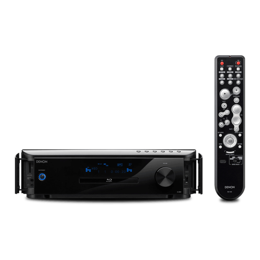
Denon S-5BD Service Manual
Blu-ray disc/dvd surround receiver
Hide thumbs
Also See for S-5BD:
- Product sheet (2 pages) ,
- Code list (2 pages) ,
- Owner's manual (95 pages)
Table of Contents
Advertisement
Quick Links
e
S-5BD
• For purposes of improvement, specifi cations and design are subject to change without notice.
• Please use this service manual with referring to the operating instructions without fail.
• Some illustrations using in this service manual are slightly different from the actual set.
S0151V03DM/DG1009
SERVICE MANUAL
MODEL
BLU-RAY DISC/DVD SURROUND RECEIVER
Copyright 2010 D&M Holdings Inc. All rights reserved.
WARNING: Violators will be prosecuted to the maximum extent possible.
JP
E3
E2
e
D&M Holdings Inc.
Ver. 3
Please refer to the
MODIFICATION NOTICE.
EK
K2A
E1
E1K EUT
Advertisement
Table of Contents

Related Manuals for Denon S-5BD


Summary of Contents for Denon S-5BD
- Page 1 MODIFICATION NOTICE. SERVICE MANUAL MODEL E1K EUT S-5BD BLU-RAY DISC/DVD SURROUND RECEIVER • For purposes of improvement, specifi cations and design are subject to change without notice. • Please use this service manual with referring to the operating instructions without fail.
-
Page 2: Safety Precautions
SAFETY PRECAUTIONS The following check should be performed for the continued protection of the customer and service technician. LEAKAGE CURRENT CHECK Before returning the unit to the customer, make sure you make either (1) a leakage current check or (2) a line to chassis resistance check. - Page 3 NOTE FOR SCHEMATIC DIAGRAM WARNING: Parts marked with this symbol z have critical characteristics. Use ONLY replacement parts recommended by the manufacture CAUTION: Before returning the unit to the customer, make sure you make either (1) a leakage current check or (2) a line to chassis resistance check. If the leakage current exceeds 0.5 milliamps, or if the resistance from chassis to either side of the power cord is less than 460 kohms, the unit is defective.
- Page 4 WARNING AND LASER SAFETY INSTRUCTIONS WARNING WAARSCHUWING All ICs and many other semi-conductors are Alle IC’s en vele andere halfgeleiders zijn susceptible to electrostatic discharges (ESD). gevoelig voor elektrostatische ontladingen Careless handling during repair can reduce (ESD). life drastically. Onzorgvuldig behandelen tijdens reparatie When repairing, make sure that you are kan de levensduur drastisch doen connected with the same potential as the...
-
Page 5: Technical Specifications
TECHNICAL SPECIFICATIONS n Audio Section n Applicable Discs/Memory Cards • Power amplifier BD-Video discs : 12 cm 1 side 1 layer, 12 cm 1 side 2 layers Rated output : DVD-Video discs : 12 cm 1 side 1 layer, 12 cm 1 side 2 layers/ Front : 75 W + 75 W (1 kHz, 4 Ω, T.H.D. 0.7 %) 12 cm 2 sides 2 layers (1 side 1 layer) Center : 75 W (1 kHz, 4 Ω, T.H.D. 0.7 %) 8 cm 1 side 1 layer, 8 cm 1 side 2 layers/ Surround : 75 W + 75 W (1 kHz, 4 Ω, T.H.D. 0.7 %) 8 cm 2 sides 2 layers (1 side 1 layer) Output connectors : Front, Center, Surround : 4 – 16 Ω Compact Discs (CD-DA) : 12 cm / 8 cm discs • Analog Memory cards : Input sensitivity/Input impedance : 160 mV/47 kΩ... - Page 6 BD/ABD-520 or BLX-108 z Refer to "MEASURING METHOD AND WAVEFORMS". Service Jigs When you repair the printing board, you can use the following JIG (Extension cable kit). Please order to Denon Official Service Distributor in your region if necessary. Extention cable kit 00D SPK- 562 TUCP CONN.
- Page 7 DISASSEMBLY • Disassemble in order of the arrow of the figure of following flow. • In the case of the re-assembling, assemble it in order of the reverse of the following flow. • In the case of the re-assembling, observe "attention of assembling" it. • I f wire bundles are untied or moved to perform adjustment or parts replacement etc., be sure to rearrange them neatly as they were originally bundled or placed afterward. Otherwise, incorrect arrangement can be a cause of noise generation. COVER SIDE-L/R CABINET TOP ASSY Refer to "DISASSEMBLY 1.CABINET TOP ASSY" and "EXPLODED VIEW" FRONT PANEL ASSY BE UNIT ASSY DIGITAL AMP UNIT ASSY Refer to "DISASSEMBLY Refer to "DISASSEMBLY Refer to "DISASSEMBLY 2.PANEL FRONT SUB ASSY"...
- Page 8 About the photos used for descriptions in the DISASSEMBLY" section. • T he direction from which the photographs used herein were photographed is indicated at "Direction of photograph: ***" at the left of the respective photographs. • Refer to the table below for a description of the direction in which the photos were taken. • Photographs for which no direction is indicated were taken from above the product. The viewpoint of each photograph Direction of photograph: B (Photografy direction) Front side [View from above] Direction of photograph: C Direction of photograph: D Direction of photograph: A 1.
- Page 9 (2) Remove the screws and the Cover Side. Direction of photograph: A (3) Remove the screws. Direction of photograph: A (4) Remove the screws. Direction of photograph: C Direction of photograph: D Please refer to "EXPLODED VIEW" for the disassembly method of each P.W.B included in CABINET TOP ASSY.
-
Page 10: Front Panel Assy
2. FRONT PANEL ASSY Proceeding : COVER SIDE-L/R CABINET TOP ASSY FRONT PANEL ASSY → → (1) Remove the Cover Tray. Direction of photograph: B (2) Remove the screws. View from bottom (3) Remove the screws. Direction of photograph: D (4) Disconnect the connector wire and FFC Cable. CY054 FFC Cable CX104 FRONT PANEL ASSY FFC Cable CY111 CHASSIS MAIN... - Page 11 3. DIGITAL AMP UNIT ASSY Proceeding : COVER SIDE-L/R CABINET TOP ASSY DIGITAL AMP UNIT ASSY → → (1) Remove the screws. Disconnect the connector wires and FFC Cable. DIGITAL AMP UNIT ASSY CX104 CY044 CY047 FFC Cable CY046 CY035 (2) Remove the screws. Direction of photograph: A 4. BE UNIT ASSY Proceeding : COVER SIDE-L/R CABINET TOP ASSY...
- Page 12 5. CHASSIS MIDDLE Proceeding : COVER SIDE-L/R CABINET TOP ASSY BE UNIT ASSY → → → CHASSIS MIDDLE (1) Remove the screws. CHASSIS MIDDLE Direction of photograph: D zIn the case of the re-assembling, assemble it in order from 1 to 6. 6.
- Page 13 7. CHASSIS BACK ASSY Proceeding : COVER SIDE-L/R CABINET TOP ASSY BE UNIT ASSY → → → CHASSIS MIDDLE → CHASSIS BACK ASSY (1) Remove the screws. Disconnect the connector wire. CHASSIS BACK ASSY CX191 CX234 CX032 (2) Remove the screws. Direction of photograph: A (3) Remove the screws. Direction of photograph: C Please refer to "EXPLODED VIEW" for the disassembly method of each P.W.B included in CHASSIS BACK ASSY.
- Page 14 8. SMPS UNIT ASSY Proceeding : COVER SIDE-L/R CABINET TOP ASSY BE UNIT ASSY → → → CHASSIS MIDDLE → CHASSIS BACK ASSY → SMPS UNIT ASSY (1) Remove the screws. Removing discs (1) Remove the screws. View from bottom (2) Slide the SLIDE CAM in the direction of the arrow. Direction of photograph: A (3) Draw out the LOADER TRAY, then remove the disc.
- Page 15 DIAGNOSTICS OF OPTICAL PICKUP AND REPLACING FE MAIN P.W.B AND BD MECHANISM UNIT ASSY Make failure diagnostics of the Optical Pickup as follows. If the laser drive current (Iop) becomes more than ±12[mA] of the initial value, the Optical Pickup should be replaced. The laser drive current initial value is checked by "Iop checked Method"...
- Page 16 1. Iop checked Method Select the laser ON/OFF(CD/DVD/BD)mode of the test mode, and check the IOP value of CD laser, DVD laser or BD laser. (Refer to "6. Test mode") FL Display (The display part of 16 digits) L a s e r O n O f f DVD laser current check Press the 8 or 9 button to display the laser current value, and then select [X].
- Page 17 SERVICE MODE s Special mode setting button Button Button Mode contents Entering the mode Backup data initialization is carried out. 1 Initialization mode SOURCE ON/STANDBY button (Remove settings for Network Setup.) Opration Heat run mode 2 Heatrun & Version display mode SOURCE AC cord Serial No.
- Page 18 2. Heat run & Version display mode 2.1. preparation (1) Equipment used : Heat run disc (This operation may not work with any discs other than the heat run discs listed below.) : CD TEST DISC (TCD-HR01) DVD : DVD TEST DISC (TDV-HR01) : BD TEST DISC (TBD-HR01) (2) Unit setting : No spec other than the following procedure.
- Page 19 Display item Display Main 1st Boot Loder M a i n F B L : X X . X X S u b : X X . X X Sub-μcom D S P : X X . X X A u d i o P L D : X X X X Audio PLD...
- Page 20 2.6. Error display See the following table for each "Error information" display and its contents (status). Display order is q , w , e , r , t . Condition State Display q Sub-μcom NG No response from Sub-μcom S U B E R R O R w DIR NG No response from DIR...
- Page 21 3. Displaying the protection history mode 3.1. preparation (1) Equipment used: None (2) Unit setting: No spec other than the following procedure. 3.2. procedure (1) Plug the AC cord into a power outlet. (2) While pressing 5 and 8 buttons simultaneously, press the ON/STANDBY button to turn the power on. The error (protection history display) mode is set.
- Page 22 3.4. Clearing the protection history There are two ways to clear the protection history, as described below. (1) Start up the error (protection history display) mode, display the error, then press and hold in the 2 button for 3 seconds. P R O T E C T H I S T O R Y : S P O U T _ D C...
- Page 23 4. KEY LOCK mode 4.1. preparation (1) Equipment used: None (2) Unit setting: No spec other than the following procedure. 4.2. procedure (1) While pressing 2 and 1 / 3 buttons simultaneously, plug the AC cord into a power outlet. (2) "KEY_LOCK_MODE"...
-
Page 24: Test Mode
5. Test mode 5.1. Entering the test mode The test mode is entered by pressing the 2 and 9 buttons simultaneously, plug the AC cord into a power outlet. FL tube display when test mode entered FL Display (The display part of 16 digits) T E S T M O D E When the test mode is set, a color bar appears on the monitor. - Page 25 5.3. About each mode ・ With the mode selected, press the 1 button to set that mode. (1) Laser on/off (CD/DVD/BD) mode Press the 8 or 9 button to select [X] and press the 1 button to set it. Laser on/off control is executed and the laser current is displayed. FL Display (The display part of 16 digits) T 2 X m m m m...
- Page 26 (3) Error rate measurement mode Press the 8 or 9 button to select [YY] . Refer to [Table 2 - Error rate details]. FL Display (The display part of 16 digits) T Y Y F F F F F F F F F F (X : measurement mode, F : Address and error rate (When not set, "F"...
- Page 27 (5) Track buffer output mode Press the 8 or 9 button to select "Y" and switch the track buffer output. FL Display (The display part of 16 digits) T E Y T r a c k B u f f (Y=1 : Track buffer being output, 0 : Track buffer output off ) When the 2 button is pressed, the layer above the current layer is displayed.
- Page 28 5.4. Stopping the mode When the 2 button is pressed, the layer above the current layer is displayed. The relationship between the different modes and the display of the different layers is shown on the table below. Mode 1 layer 2 layer 3 layer Laser on/off (CD/DVD/BD) mode...
- Page 29 Name Address range Meaning BUF_ID_SVO_SVRAM 0x000000 ~ 0x0005FF SVRAM T57A BUF_ID_SVO_CRAM0 0x000000 ~ 0x0001FF CRAM0 T57B BUF_ID_SVO_CRAM1 0x000000 ~ 0x0001FF CRAM1 T57C BUF_ID_SVO_CRAM2 0x000000 ~ 0x0001FF CRAM2 T57D BUF_ID_SVO_CRAM3 0x000000 ~ 0x0001FF CRAM3 T58A BUF_ID_SVO_ZRAM0 0x000000 ~ 0x0001FF ZRAM0 T58B BUF_ID_SVO_ZRAM1 0x000000 ~...
- Page 30 Error rate display details for each media type Measurement Remarks position When this is selected for 2-layer DVD, The inner it shifts to YY=85. BIS error detection circumference of It is invalid. It is invalid. signed number When this is selected for 1-layer DVD 2-layer or CD, it shifts to YY=73.
- Page 31 Table 3: Error log details Contents Error log No. Remarks (Error log overall layout) LD On Time (4Byte) Error type (2Byte) See "Table 3-1: Error type details" 3 (31 to 34 displayed in 4-byte units) Reserve (16Byte) Media type (2Byte) See "Table 3-2: Media type details"...
- Page 32 ABOUT REPLACE THE MICROPROCESSOR WITH A NEW ONE When replaced of the U-PRO (Microprocessor) or the Flash ROM, confirm contents of the following. After PWB Name Ref. No. Description Remark replaced MAIN IC401 R5F64169DFD SOFTWARE: Main MAIN IC302 EN29LV160BB-70TIP SOFTWARE: MainROM MAIN IC702 MX29LV160DTTI...
- Page 33 Make a note of the settings before updating, and set them again after updating. 1.3. About the error code See the chart below for error codes, details of faults, and coping strategies when firmware updates are performed through DPMS (Denon Product Management Server). Error Details of Error code...
- Page 34 Error Details of Error code Display Coping strategies Code Error codes when rewriting B/E * * * The rewriting of block data failed Turn the power off then back on. when rewriting B/E. Updating starts automatically. U p d a t i n g f a i l Error codes when rewriting F/E The rewriting of block data failed...
- Page 35 Error Details of Error code Display Coping strategies Code General error codes when rewriting ROM other than MAIN. Failed to receive the rewrite starting M a i n R O M * * * command sent from BD SYSTEM Turn the power off then back on. CPU to MAIN CPU (when timed Updating starts automatically.
- Page 36 Error Details of Error code Display Coping strategies Code SUB CPU, DSP, FPGA, PLD failed S u b * * * to receive firmware for rewriting Turn the power off then back on. sent from BD SYSTEM CPU (when Updating starts automatically. U p d a t i n g f a i l a Check Sum error)
- Page 37 Error Details of Error code Display Coping strategies Code Error codes when rewriting SYSTEM CPU BE failed to receive firmware for S y s * * * Turn the power off then back on. rewriting sent from BD SYSTEM Updating starts automatically. U p d a t i n g f a i l CPU (when timed out).
-
Page 38: Trouble Shooting
TROUBLE SHOOTING 1. POWER 1.1. Power not turn on Power not turn on Are there any incomplete Is the ON/STANDBY connections in the Is there a short circuit Correct the short circuit indicator on the front panel connectors connecting between the speaker between the speaker and flashing red? between the various circuit... - Page 39 2. HDMI/DVI 2.1. No picture or sound is output (BD Drive) Check Supply Voltages from Power Supply Unit Check Soldering and Wires from Power Supply Unit N.G. • +5V_D4, +3.3V_D1 • [CX088] 3,4,1Pin Check Supply Control signal to Power Supply unit Check Soldering •...
- Page 40 Is the BD/DVD player's HDMI referring to the BD/DVD output setting correct? player's operating instructions. When using a DENON BD/DVD player's, is the fluorescent display tube's "HDMI" indicator lit? If using a non-DENON BD/DVD player's, proceed to "YES". Are the picture and sound...
- Page 41 The BD/DVD player does not recognize the connection with the set. When using a DENON BD/ Is the HDMI connector The pattern and circuit from DVD player, is the fluorescent (JK502/JK503/JK451) pin the HDMI connector (JK502/ display tube's "HDMI"...
-
Page 42: Analog Video
Check Output of AMP N.G. Input : IC701-6pin Check soldering of IC701 Output : IC701-29,30pin O.K. Check cable between S-5BD and monitor or Check monitor 3.2. HDMI OUT,Output NG Input N.G. Check +5V_V1 To troubleshooting 1.1.Power not turn on. +5V_V1 : CY191-5,6pin O.K. - Page 43 4. DIGITAL AMP UNIT 4.1. 8U-210080-1 No sound from the speakers. Protector operates. After the power is turned on, is the power supply to each AMP IC normally supplied? Check the source of the power supply. CY044(1),(2)pin : +47V (8U-210078 SMPS UNIT) CX211(13),(14)pin : +12V After the power is turned on, is the RESET signal to each AMP IC released?
-
Page 44: Analog Audio
5. Analog audio 5.1. 8U-210078-2 No sound is output Is the voltage of ±7V supplied to The power supply of ±7V is repaired. 8U-210078-2 CX194? Is the audio signal transmitted to The power amplifier is repaired. 8U-210080-1 CY193? Connect the connectors properly. Is the connector correctly connected Is the audio signal transmitted to with ucom board (8U-210079-1 &... - Page 45 6. FE/SACD UNIT (8U-310037) 6.1. BD or DVD or CD check Check HF signal N.G. Defect of primary circuit component. 8U-310037 (FE/SACD UNIT) 8U-310037 (FE/SACD UNIT) "MEASURING METHOD AND WAVEFORMS" • [IC100] [CX0451] and Other Circuits • Check q HF Waveform O.K.
- Page 46 CHECK LIST FOR AFTER-REPAIR-CHECK n n AdjustingnthenMasternVolume 1-1 BD and DVD VOL df Press Prepare for playback. n n StopnPlaybackn(ResumenFunction) Turn on the TV and subwoofer power. Press Change the TV input to the input of this unit. n n PausenPlayback Press Press to turn on power to Front n n Step-by-StepnPlayback the unit. During pause, press Insert a disc.
- Page 47 1-2 CD 2. USB Prepare for playback. Connect the iPod to the USB Front port . Turn on the subwoofer power. Playback starts automatically. Press to turn on power to Front the unit. iPod Insert a disc. Now Playing • Press 5 on the main unit to open/ Song close the disc tray.
- Page 48 Track Track Track 3. SD CARD 4. ANALOG AUDIO/VIDEO Input BD/SD Press to select “Disc DENON Control dock for iPod usable on this unit Front • ASD-11R/ASD-3N/ASD-3W/ASD-51N/ASD-51W Mode” or “SD Mode”. ListeningntonMusicnonnanniPod ® When playing back files Disc Mode stored on a DVD or CD. Prepare for playback. SD Mode When playing back files...
- Page 49 5. TUNER 6. HDMI1/HDMI2/F.HDMI Input Press the input source select button TUNER Press to select “FM” or Front Front HDMI ) to be played back. “AM”. The desired input source can be selected directly. When listening to an FM broadcast. When listening to an AM broadcast. Tune in the desired broadcast Youncannalsonusenthenfollowingnoperationntonselectnanninputn station.
- Page 50 MEASURING METHOD AND WAVEFORMS Measuring Disc: CD/TCD-784 DVD/VT502 or TDV-520A BD/ABD-520 or BLX-108 To check the waveforms on the FE/SACD UNIT, the GND (-) probe to " Q7 V C" point. q ~ Q6 points have the certain test points shown below. •...
- Page 51 BD PLAY Disc : ABD-520 HF wave form BD PLAY (INNER) Q1 SPD q ATEST Q2 FG BD LOADING → PLAY BD SEARCH (INNER → OUTER) Q3 SLED+ w FODP Q4 SLED- e FCS1+ Q5 SL1+ r FCS1- Q6 SL2- BD LOADING →...
- Page 52 DVD PLAY Disc : TDV-520A HF wave form DVD PLAY (INNER) Q1 SPD q ATEST Q2 FG DVD LOADING → PLAY DVD SEARCH (INNER → OUTER) Q3 SLED+ w FODP Q4 SLED- e FCS1+ Q5 SL1+ r FCS1- Q6 SL2- DVD LOADING →...
- Page 53 CD PLAY Disc: TCD-784 HF wave form CD PLAY (INNER) Q1 SPD q ATEST Q2 FG CD LOADING → PLAY CD SEARCH (INNER → OUTER) Q3 SLED+ w FODP Q4 SLED- e FCS1+ Q5 SL1+ r FCS1- Q6 SL2- CD LOADING →...
- Page 54 ANALOG VIDEO OUTPUT SIGNAL Signal: Color Bar 100% S5BD Oscilloscope 75ohm Loard Composite...
- Page 55 BLOCK DIAGRAM BD_B/E Unit BD_F/E Unit Digital Unit(1/2) AUDIO HDMI HDMI Transmitter Transmitter SiI9134 VIDEO ADV7510 HDMI ×2 VIDEO HDMI 1 HDMI Reciever Driver w/SW ADV7840 BH7868(NJM2556) AUDIO CVBS HDMI 2 Hospitality HDMI Front In Buffer HDMI 3 ADV8195 With Driver FUTABA F.HDMI Unit Display Unit...
- Page 56 POWER SUPPLY BLOCK DIAGRAM...
- Page 57 LEVEL DIAGRAMS (1/5) FRONT LEVEL DIAGRAM S-5BD LEVEL DIAGRAM FRONT ch R2A15218FP +29dB SPEAKER + LINE IN + GAIN ADAU132 ADJ. + - - + 102ohm D/A OUT - - VOLUME Display"63" + MUTE MUTE (-18dB from Max) -12.2dB -...
- Page 58 LEVEL DIAGRAMS (2/5) CENTER LEVEL DIAGRAM S-5BD LEVEL DIAGRAM CENTER ch R2A15218FP SPEAKER + GAIN ADAU132 ADJ. + D/A OUT + - VOLUME Display"63" MUTE (-18dB from Max) - +30dB NON CLIP MAX SIGNAL LEVEL 4.0Vrms SP OUT 2.52Vrms/4Ω Config1 DOLBY LIMIT LEVEL (ALLch-3dBFS)
- Page 59 LEVEL DIAGRAMS (3/5) SURROUND LEVEL DIAGRAM S-5BD LEVEL DIAGRAM SURROUND ch R2A15218FP SPEAKER + GAIN ADAU132 ADJ. + D/A OUT + - VOLUME Display"63" MUTE (-18dB from Max) - +30dB NON CLIP MAX SIGNAL LEVEL 4.0Vrms Config1 DOLBY LIMIT LEVEL 1.41Vrms(ALLch-3dBFS) SP OUT 2.52Vrms/4Ω...
- Page 60 LEVEL DIAGRAMS (4/5) SURROUND BACK LEVEL DIAGRAM S-5BD LEVEL DIAGRAM SURR.BACK ch R2A15215FP PRE OUT MUTE GAIN ADAU132 ADJ. + D/A OUT + - VOLUME Display"63" MUTE (-18dB from Max) - +30dB NON CLIP MAX SIGNAL LEVEL 4.0Vrms Config1 DOLBY LIMIT LEVEL 1.41Vrms(ALLch-3dBFS) 0dBFS 0.88Vrms...
- Page 61 LEVEL DIAGRAMS (5/5) SUB WOOFER LEVEL DIAGRAM S-5BD LEVEL DIAGRAM SUBWOOFER ch R2A15218FP - MUTE PREOUT GAIN ADJ. + D/A OUT ADAU1328 + - - - - MUTE VOLUME Display"63" ADAU1328 - (-18dB from Max) +30dB Config2 DOLBY LIMIT LEVEL (ALLch-3dBFS) SUM to FRONTch 3.876V...
- Page 62 PRINTED WIRING BOARDS 8U-210078-1 (COMPONENT SIDE) C231 C227 C244 C225 C258 C223 CX191 CX234 D140 T103 D141 ZD119 C278 D143 D142 TR121 C273 TR120 L110 L103 R206 IC105 R195 TR134 C174 R193 R194 R182 D133 IC107 ST101 D132 ZD118 R196 R186 C177 TR113...
- Page 63 8U-210078-1 (FOIL SIDE) C253 C238 C248 C247 C239 C252 C230 C232 C234 C235 C262 C245 C240 C243 C242 C259 C255 C249 C257 C261 C254 C241 C181 C233 C180 C179 C272 R919 TR128 R200 C271 R207 C189 C175 TR132 C182 R205 R173 R204 R162...
- Page 64 8U-210078-2 (COMPONENT SIDE) 8U-210078-3 (COMPONENT SIDE) 8U-210078-3 (FOIL SIDE) S701 C703 CY281 C429 C390 C389 C431 C430 C399 TR314 C398 ST402 C388 C704 ST401 C437 C434 C479 TR601 R703 TR309 R382 TR311 TR334 TR313 R485 C395 C377 C396 R620 TR332 C412 C406 C404...
- Page 65 8U-210079-1 (COMPONENT SIDE) CX034 CY191 CY234 ST101 TR101 D101 C231 C251 TR102 C233 C229 D112 C245 C267 C247 C243 C261 C237 C263 C259 C232 C230 C246 D111 TR103 C244 C262 C260 C236 C235 C234 C108 C107 C249 C248 C250 R164 R153 R130 C266...
- Page 66 8U-210079-1 (FOIL SIDE) CC106 C103 CC105 CC107 C102 IC104 R190 CC104 C101 R129 R185 R166 R151 R204 R184 R186 D113 IC105 R202 C192 C197 C128 C223 C222 C198 C127 C220 C199 C126 C427 C425 C428 C424 C422 C429 C765 R413 IC706 R412 R757...
- Page 67 8U-210079-3 (COMPONENT SIDE) 8U-210079-4 (COMPONENT SIDE) 8U-210079-3 S851 R886 S852 JOINT(B) UNIT ST902 R880 OP/CL S856 PLAY R881 R885 R878 S854 R877 STOP CX185 CX092 CX183 CX081 R874 R873 R872 S855 R871 8U-210079-4 W853 C894 C893 S853 CX045 SOURCE KEY UNIT CY107 CY101 CY194...
- Page 68 8U-210080-1 (COMPONENT SIDE) CY193 C144 C132 C401 TR301 TR305 TR302 C355 C354 C351 C350 W604 DIGITAL AMP UNIT C452 632010080103D C451 CX104 C450 8U-210080-1 C116 C106 C250 C218 IC101 C283 C172 C219 C169 C220 CX046 RL401 C221 R180 R179 R174 R149 R165 R121...
- Page 69 8U-210080-1 (FOIL SIDE) C123 C125 C140 C120 C129 C143 C138 C141 R160 R336 R334 R335 C347 C348 C352 R348 R337 R338 R347 R339 R349 D301 D304 R342 R352 C349 C353 TR110 C136 C133 C104 C109 C113 C101 C102 C112 C103 C110 TR102 TR104...
- Page 70 8U-210080-2 (COMPONENT SIDE) 8U-210080-3 (COMPONENT SIDE) 8U-210080-4 (COMPONENT SIDE) 8U-210080-5 (COMPONENT SIDE) SD/MIC/HP UNIT C525 JK502 8U-210080-3 C515 FB501 ZD502 C511 C516 CY152 C510 D512 CC513 FB503 CC516 CX084 CC514 C512 CC509 D509 ST602 CC515 D510 C502 CC522 CC508 D507 CC521 D508 CX105...
- Page 71 8U-310036 (FOIL SIDE) 8U-210080-6 (COMPONENT SIDE) 8U-210080-7 (COMPONENT SIDE) Bside R361 C361 C384 CY192 C901 C902 C926 C927 C997 C996 C928 C951 C929 C952 C954 C930 RA301 RA303 C955 C931 C932 RA211 RA300 RA302 C953 C223 RA210 C806 C224 RA209 R494 R492 TR304...
- Page 72 8U-310035 (COMPONENT SIDE) 8U-310035 (FOIL SIDE) ST102 R718 CX094 R755 R756 R722 RR161 RR133 RR132 RR131 RR130 C182 C726 CC563 C162 C161 C160 C159 R731 D706 CC433 RR160 C732 R711 C814 C184 RR184 RR448 RR677 CC696 CC695 RR692 RR449 C181 C771 RR810 RR611...
- Page 73 5A 250V 215 F101 2061099058 E1,E2 4A 250V 215 T4AH250V C132 0.01/630V FH101 FF101 T102 +47V_D L108 L107 R170 0.22 FUSE_CLIP FUSE_CLIP CX032 CY031 CX031 HR28R-E123 SW-TRANS(ST-4154A) L102 HR28R-E123 R171 2P-VHw 3P-SDN R918 R172 OPEN CX044 INDUCTOR-7G14D-100M 4P-VH D120 FML-4202S MTZJ33B MTZJ24B +42V_D...
- Page 74 KSE TUNER bd210079.cir/007.sht +7V_A1 -7V_A1 8U-210079-3 +9V_TU JOINT(B) UNIT TUNER CX112 R320 C387 10/50 C464 1000P C476 1000P 11P-FFCs R321 R335 100 +3.3V R364 C385 10/50 CX101 C465 0.01Z C477 0.01Z PORT_SEL CX107 10P-SOCKET 10P-SOCKET TR304 C466 0.1Z C478 0.1Z TR301 0.1Z OPEN...
- Page 75 MICSIG MICSIG +7V_A1 IC601 C608 C601 R620 NJM4556AD TR605 H/PR HP_R (1/2) GND_A R611 R613 HP_L R607 R617 R601 C603 100P TR603 R602 C604 100P R614 R618 R608 C609 GND_A1. TR604 KTC2875B (2/2) C602 TR606 R612 R619 H/PL C607 KTC2875B IC601 0.1Z NJM4556AD...
- Page 76 210078-3 ON/ST UNIT CY048 4P-PHs bd310036.cir/005.sht 8U-310036 BE UNIT 8U-210078-4 CVBS OUT UNIT ON/STB C711 10/50 IC701 CY094 C706 BH7868FS 9P-PHs 0.01 C705 +5V_V1 C707 1000P 1 VCC1 JK701 C716 R713 C709 0.1Z C715 RCA-117-02(1P-YEL) 2 S1 Y_BD 0.1 1000/6.3 CVBS OUT 3 S2 GND_V1...
- Page 77 bd210080.cir/001.sht bd210079.cir/007.sht bd210080.cir/005.sht bd210080.cir/004.sht 8U-210080-1 8U-210079-3 8U-210080-5 8U-210080-2 D.AMP UNIT JOINT (B) UNIT JOINT (C) UNIT F.HDMI UNIT +9V_A1 CY155 CX085 CX184 8P-HEADER 15P-HEADER R106 18P-HEADER OPEN CX091 CY108 9P-HEADER CY102 R107 10P-HEADER CY211 OPEN 10P-HEADER CX188 FCZ100E-21SS-K 18P-HEADER TR105 RTF010P02 +9V_TU C209...
- Page 78 TO_CPU_CONNECT BLOCK bd210079.cir/001.sht A.AUDIO UNIT iPOD 232C/REMOTE/TRIG POWER ON/OFF D_AMP To FRONT UNIT DIGITAL SP_RL PREMUTE E.VOL TUNER PACK LIMIT C315 1000P C318 1000P C316 0.01Z C319 0.01Z C317 0.1Z C320 0.1Z GND_A1 GND_D1 GND_A1 GND_D1 ON/OFF3.3V/A0 R322 OPEN Q_STBY_POWER R323 OPEN ON/OFF5V/RD...
- Page 79 bd210079.cir/002.sht TO_LEVEL_CHG BLOCK iPOD Extended ROM FRONT UNIT 232C DIGITAL REMOTE TUNER D_AMP E.VOL EXPOUT R456 10K R545 10K R546 R457 10K R547 R458 10KR548 R459 R549 R544 R540 R541 R437 R542 GND_D1 GND_D1 BD_RST ROMPOWER R498 R526 4.7K 4.7K P11/D9 P43/A19 MODE2/D8...
- Page 80 bd210079.cir/003.sht bd210079.cir/003.sht IC609 8U-210079-1 8U-210079-1 PQ050DNA1ZPH JTAG MAIN CPU BLOCK MAIN CPU BLOCK VOUT ON/OFF IC605 C680 C676 C679 AK4424ET 1u/10 1u/10 C714 0.1Z C715 0.01 RR604 VSS2 C716 1000P RR606 C686 10/16 CVDD USB_L MCLK MCLK BCKo RR608 BICK VSS1 Aout RR609...
- Page 81 +5.0V_V1 C833 47/10 C834 RR801 C827 MUTEA 1/50 CX302 R814 bd210079.cir/001.sht DIN-409A(1P-S-TERM) MIXO1 CC803 8U-210079-1 V_AUX MIXO2 CPU CONNECT BLOCK MUTEB RR802 C826 RR805 R815 IC802 OPEN_R BA7664AFV CC804 RR806 R801 R802 R804 RR803 RR804 ETHERNET 75(1%) 75(1%) OPEN OPEN OPEN OPEN CX121...
- Page 82 210079-4 bd210079.cir/001.sht CX045 OPEN/CLOSE SOURCE STOP 8U-210079-1 4P-PH KEY UNIT R871 R873 R877 R880 R885 MAIN UNIT 1.3K 1.3K CPU CONNECT BLOCK KEY1 bd210079.cir/001.sht GND_D1 8U-210079-1 KEY2 MAIN UNIT GND_D1 CPU CONNECT BLOCK R872 R874 R878 R881 R886 1.3K 1.3K C876 0.1Z C877 0.01Z...
- Page 83 JOINT(B) UNIT 8U-210079-3 USB_L USB_L GND_A1 GND_A1 USB_R USB_R GND_D1 GND_D1 BDMIXL BDMIXL GND_A1 GND_A1 BDMIXR BDMIXR VOLMUTE VOLMUTE VOLCLK VOLCLK VOLDATA VOLDATA +9V_TU +9V_TU +9V_TU +9V_TU T.MUTE T.MUTE TUNED TUNED bd210078.cir/002.sht STEREO STEREO 8U-210078-2 TU_SDA TU_SDA TU_SCL TU_SCL AUDIO UNIT RDS_CLK RDS_CLK RDS_DATA...
- Page 84 +12V_D1SW +42V_D1 +4V_A1 +7V_A1 +42V_D1 IC101 CY044 4P-VH IL1117H-3.3ET L101 R184 C227 C204 10/50 INDUCTOR-7G14J-100M-R AS101 ASS4000000 +42V_D AMP-RADIATOR 1200/63 bd210099.cir/001.sht +42V_D 8U-210099 R183 C203 0.01 GND_A C231 SMPS UNIT GND_D1 GND_D1 GND_D RESET GND_D1 TR106 47/16 C232 KRA102S C195 330P +7V_A1 TR101...
- Page 85 +42V_D1 +12V_D1SW L301 R326 C331 INDUCTOR-7G14J-100M-R C318 10/50 1200/63 bd210080.cir/003.sht C317 0.01 C332 8U-210080-1 R325 GND_A DIGITAL AMP UNIT(3/3) GND_D C313 330P C333 47/16 C340 1200/63 +4V_A1 C CH R309 C339 R312 R303 5.6K OC_ADJ R305 R307 5.6K C314 100P C305 100P C302...
- Page 86 CX046 CY046 4P-SDN 4P-VH RL401 (From the front) bd210080.cir/001.sht 8U-210080-1 DIGITAL AMP UNIT(1/3) CX047 CY047 4P-SDN 4P-VH RL402 RL403 bd210080.cir/002.sht 8U-210080-1 DIGITAL AMP UNIT(2/3) (From the front) +12V_D1SW 3P-SDN 3P-VH CX035 CY035 TR401 TR402 TR403 TR404 TR405 KRC102S KRC102S KRC102S KRC102S KRC102S GND_D1...
- Page 87 ZD502 OPEN GND_D1 11A121 FB501 FB502 HP_L 11A121 H/P OUT HP_R 11A121 FB503 H/PDET R539 GND_HP H/P-JACK(D3.5-SW) 0.1Z C510 R540 JK502 0.1Z C511 47/6.3 C512 D513 D514 0.1Z C513 OPEN C514 RR501 RR502 RR505 RR506 JK451 OPEN_R HDMI-SOCKET(YKF45-7041V) SHELL2 TR502 HPDET HPDF KRC102S...
- Page 88 JOINT(C) UNIT MAIN 8U-210080-5 W601 BRACKET-SCREW VOLUME C610 S601 0.01Z ROTARY-ENC. W602 R603 OPEN. VOL_A. CY041 4P-JB R604 VOL_B. SWM3.3V VOL_A. CX084 bd210079.cir/006.sht FG11 VOL_A 8P-HEADER 8U-210079-2 VOL_B. VOL_B FLD UNIT DGND DGND GND_D1 8U-210080-4 DGND DGND bd210079.cir/001.sht DDC_SCK DDC_SCK bd310036.cir/009.sht 8U-210079-1 8U-310036...
- Page 89 TO GUI TO SUBCPU TO HDMI RX SUBCPU (sht6) (sht4) (sht6) (sht3) (for Writing) IC104 PQ033DNA1ZPH VOUT ON/OFF RR136 OPEN RE105 RR137 OPEN SWSUM R183 RR140 RR166 RR124 5.6K 5.6K CX872 C143 SBCK R159 0 7P-FFC C171 RR114 C153 RR141 1000P +3.3V_D1SW OPEN...
- Page 90 TO SUB CPU (sht6) TO DIR/CODEC sht1 RR255 RR256 TR201 OPEN +3.3V_D1SW R204 OPEN C207 OPEN R208 OPEN DSPPWR D3.3V TR202 D1.2V R206 OPEN OPEN D201 RR209 33 OPEN RR210 33 CLKO R202 RR211 33 SDA10 R214 RR212 33 1.2V RR213 33 SDWE RR258...
- Page 91 TXEN TXEN TXEN HPDF HPD6 HPD6 RS553 CEC_COM DDCA_SDA 498mA D536 OPEN. DDCA_SDA FB501 DDCA_SCL TK73318WTL-G DDCA_SCL 260mA BLM21PG221 RXD5V RS546 IC501 IC501 IC501 IC501 IC501 IC501 IC501 IC501 IC501 IC501 IC501 IC501 IC501 IC501 IC501 IC501 IC501 IC501 IC501 RXD5V RXA_5V CEC3.3V...
- Page 92 NEW!! IC956 PQ12GN01ZPH +3.3V_IO +1.2V_INT DGND FB614 FB612 BIAS 11A121 18PG121 DGND +1.2V_DPLL3 +1.2V_APLL1 +1.2V_APLL3 +1.2V_DPLL1 FB606 FB604 FB608 FB610 11A121 11A121 11A121 11A121 IPOPCK1 IPOPCK2 IC605 EP2C35F484 VIEW +1.2V_APLL2 +1.2V_APLL4 +1.2V_DPLL2 +1.2V_DPLL4 RR504 HRPCK1 RR553 OPEN RR505 FB611 HRPCK2 FB605 FB607 FB609...
- Page 93 R717 OPEN R718 OPEN R755 R756 C777 10/6.3 C779 1000P R725 C780 1000P OPEN R711 D706 OPEN_R R722 OPEN CEC_CLK DVDD C782 DVDD DVDD R731 HTG5 CEC_IN HTPCK DVDD_3V HTG4 R726 HTG3 1TXINT JK701 HTG2 19P-HDMI-CON(2LINE) HTG1 TX2+ TX2+ HTG0 R743 CC703 TX2-...
- Page 94 TO HDMI RX (sht3) TO GUI (sht4) TO HDMI RX (sht3) TO HDMI Tx (sht5) TO HDMI Tx (sht5) FB901 BLM21PG221 R987 R988 CEC_POWER C922 CK4.7 C923 CK4.7 R991 C924 CK0.1 100K R954 CY185 R955 18P-SOCKET TXEN TXEN HPD6 1 NC(SW) AVIN HPDF CEC_COM...
- Page 95 SERIAL/GPIO C142 1000P IDE -> sht005 ETHER -> sht005 JTAG/TESTMODE -> sht005 SERIAL I/F(SCIF) -> sht005 C143 0.01Z B_OK B_OK G_OK A_OK F_OK(SET2) D_OK(SET1) H_OK(SET1) AL33 RESET_N AT1DATA0 SH_GPIO7[0] RESET_N JTAG_SH4 AT1DATA0 SH_GPIO7[0] ECOL SCIFSCK MPMD AT1DATA1 SH_GPIO7[1] MPMD AJ32 C144 0.1Z SCIFSCK...
- Page 96 DA0A13 DA0A11 +1.8V_D4 DA0A13 DA0A11 +1.8V_D4 +1.8V_D4 +1.8V_D4 DA0A13 DA0A11 RA150 22x4 DA0A13 DA0A11 SDA0A13 DA0A13 DA0A11 SDA0A11 SDA0A6 SDA0BA0 DA0BA0 DA0A6 DA0BA0 DA0A6 DA0BA0 DA0A6 DA0BA0 DA0A6 DA0BA0 DA0A6 GND_D4 GND_D4 GND_D4 DA0A0 DA0A10 GND_D4 DA0A0 DA0A10 DA0A0 DA0A10 RA151 22x4 DA0A0...
- Page 97 DA1A11 DA1A13 RA200 DA1A11 DA1A13 22x4 DA1A11 DA1A13 SDA1A11 +1.8V_D4 SDA1A13 +1.8V_D4 SDA1A4 SDA1BA2 DA1BA2 DA1A4 DA1BA2 DA1A4 DA1A4 DA1BA2 DA1WE_N DA1BA1 RA201 22x4 DA1WE_N DA1BA1 GND_D4 GND_D4 SDA1WE_N DA1WE_N DA1BA1 SDA1BA1 SDA1BA0 SDA1A6 DA1A6 DA1BA0 DA1A6 DA1BA0 DA1A6 DA1BA0 +1.8V_D4 +1.8V_D4 +1.8V_D4...
- Page 98 sht.005 RESETb HADRS0 +3.3V_D4 HADRS1 HADRS1 HADRS2 HADRS2 1Gbits HADRS3 HADRS3 Flash HADRS17 HADRS4 HADRS26 HADRS4 HADRS25 HADRS5 HADRS5 IC110 HADRS6 HADRS6 S29GL01GP11TFCR20# R270 R271 HADRS7 HADRS7 HADRS24 HADRS23 R272 HADRS8 HADRS8 HADRS16 HADRS9 R273 HADRS9 HADRS15 BYTE# HADRS14 HADRS10 HADRS10 HADRS13 HDATA15...
- Page 99 +3.3V_D4 ST903 STYLE-PIN CX048 +5.0V_V1 4P-ZH +3.3V_D4 RA302 RA300 RA301 RA303 bd210078.cir/004.sht 22Kx4 22Kx4 22Kx4 22Kx4 8U-210078-4 CVBS OUT UNIT R497 R495 CY452 C368 TPX301 R484 45P-FFC R485 R489 R491 R303 TPX302 OPEN OPEN TR303 PD0. R434 HDREXT AT1DATA0 2SA1022 R305 PD1.
- Page 100 +3.3V_NSW +5V_D4 POWER CX088 20022WS-8C W653 OPEN +3.3V_D1 +3.3V_D4 GND_D1 FB901 FBMJ1608HS280NT +5.0V_BD W201 +5.0V_BD OPEN R920 OPEN R969 FB910 GND_D1 FBMJ1608HS280NT GND_D1 DAC_AVDD33 R921 OPEN R970 BD_P_DOWN BD_POWER W209 sheet.001 R923 FB911 C974 1000P OPEN FBMJ1608HS280NT GND_D4 C975 0.01 PLL_AVDD33 C976 R924...
- Page 101 +3.3V_NSW6 +3.3V_D6 +3.3V_NSW6 +3.3V_NSW +5V_D4 C810 0.1Z HARD_REV IC852 S-24CS08AFJ GND_D4 R812 R822 R828 R834 R841 R847 R855 OPEN_R OPEN_R OPEN_R OPEN_R OPEN_R OPEN_R OPEN_R R803 OPEN_R FE_RX FE_TX sht.005 TEMPDET GND_D4 LD_OPEN_N REGIONN_BD R813 R823 R829 R835 R842 R848 R856 OPEN_R OPEN_R...
- Page 102 ucom sheet7 +3.3V_D4 to B/E sht.001 R716 OPEN +3.3V_D4 FB700 IC718 C717 OPEN R701 OPEN OPEN R712 OPEN CLK54M R719 VDD54M R713 OPEN VMCLK R702 VSS54M C704 R720 FSEL 768FS R709 OPEN IC715 R707 OPEN OPEN TEST SM8707HV-G AMCLK1 R700 R721 AVDD VDD1...
- Page 103 +1.8V_D4 +3.3V_D4 +5V_D4 FB512 FBMJ1608HS280NT FB513 FBMJ1608HS280NT FB510 FBMJ1608HS280NT R549 1HTINT SH_GPIO5[5] FB511 R552 1HT_RST M32_GPIO[4] FBMJ1608HS280NT R550 RLT_SCL SH_GPIO4[1] RLT_SDA R551 FB514 SH_GPIO4[0] R521 R523 R520 FBMJ1608HS280NT C505 CK1000P C522 CK1000P CK1000P C523 C506 CK0.1 C507 CK0.1 R512 4.7K ST901 CVCC18 CI2CA...
- Page 104 TO sheet 002 (A4) TO sheet 02(A6) +3.3V_A1 +8V_P1 +3.3V_D1 +1.5V_A1 +1.5V_D1 +5V_P1 +3.3V_A1 CX451 +5V_A1 45P-FFCs (5F2.2535C) FCS1+ FCS1+ FCS1- FCS1- TRK+ TRK+ C162 TRK- TRK- 0.01Z FCS2- FCS2- C186 FCS2+ C119 0.022 FB106 0.01Z FCS2+ EXPA- C118 1u/10 EXP_A- R155 EXPB-...
- Page 105 TO sheet001(A7) TO sheet 001(A11) +3.3V_D1 +1.8V_D1 CX403 X301 OPEN 25.0MHz CX052 RESTn OPEN DD7. DD8. C320 DD6. 0.01Z R301 OPEN DD9. GND_D C324 FB301 R302 OPEN (GND_A1) 0.1Z DD5. DD10. R325 DD10 R348 DD4. RESET_n C325 C301 0.1Z DD11. 100/6.3 DD11 R349...
- Page 106 +2.5V_A3 IC504 IC504 IC504 IC504 OPEN OPEN OPEN R438 R440 OPEN R454 R456 OPEN OPEN OPEN OPEN TO FE (SHEET1) R458 OPEN PLCK R457 R439 R441 R455 +2.5V_D3 +3.3V_D3 OPEN OPEN OPEN OPEN GND_A3 +3.3V_D3 C418 C426 OPEN OPEN IC504 OPEN R452 RA401...
- Page 107 +3.3V_D3 +3.3V_D3 VCCO_3 (BANK2) (BANK0) F_A21 P11 R697 OPEN F_CEN D14 F_A22 R11 R654 R698 OPEN OPEN R565 OPEN F_BYTEN C15 F_OEN C16 RSV0_15 R579 OPEN RSV2_07 R566 OPEN F_A23 R10 RSV0_16 R580 OPEN RSV2_08 P13 R567 OPEN RSV0_17 R581 OPEN RSV2_09 +3.3V_D3...
- Page 108 +3.3V_D4 FB932 BLM18PG330SN1 R812 IDE_DD_0 R813 IDE_DD_1 R814 IDE_DD_2 R815 IDE_DD_3 ATAPI R816 IDE_DD_4 R817 IDE_DD_5 R818 IDE_DD_6 RESET_n RESET_n R819 IDE_DD_7 CX452 R820 IDE_DD_8 45P-FFCs (5F2.2535C) R821 IDE_DD_9 IC904 DD10 R822 IDE_DD_10 OPEN IDE_DD_0 R968 DD00 DD11 R823 IDE_DD_11 IDE_DD_1 R969 DD01...
- Page 109 R998 MVPOWER (SHEET5) FB910 BLM18PG330SN1 40mA +5V_P1 D906 1SS355 FB914 FB919 BLM18PG330SN1 424mA +8V_P1 VOUT VIN 8 NC 7 (SHEET1) NC 6 CONT 5 IC304 MM1825YHBE FB917 BLM18PG330SN1 GND_D (GND_P1) FB918 BLM18PG330SN1 MOTOR +12V_M1 R927 FB937 IC907 OPEN BLM18PG330SN1 +5V_M1 VCC 2 (SHEET1) FB922...
- Page 110 WIRING DIAGRAM CX185 CX092 210079 CX091 GND_V1 JOINT(B) UNIT 2/3 Sheild Cable Y_BD CY091 GND_V1 CY184 C_BD GND_V1 V_AUX GND_V1 CX184 CX131 CX173 CX106 CX054 CX085 CX111 GND_V1 +5.0V_V1 CX183 GUI/OSD_RST CX188 GUI/OSD_CLK GUI/OSD_TX CY188 Cable GUI/OSD_RX GUI/OSD_REQ GUI/OSD_ACK BDOWNSUB B/P Panel Side→...
- Page 111 EXPLODED VIEW 45 *2 66 *4 38 *3 21-3 21-4 23-2 23-1 21-1 21-2 7 *4 20-5 20-2 21-2 20-1 20-6 21-3 20-3 21-4 20-4 21-1 24-2 24-1 WARNING: Parts marked with this symbol have critical characteristics. Use ONLY replacement parts recommended by the manufacturer.
- Page 112 PARTS LIST OF EXPLODED VIEW Ref. No. Part No. Part Name Remarks Q'ty 21-1 ARM DOOR 2547210071000S zParts for which "nsp" is indicated on this table cannot be supplied. 21-2 CUSHION ARM DOOR-A 4050212795000S zP.W.B. ASS'Y for which "nsp" is indicated on this table cannot be supplied. When repairing the P.W.B. ASS'Y, check the board parts table and order replacement parts. zThe parts listed below are for maintenance only, might differ from the parts used in the unit in appearances or dimensions.
- Page 113 Ref. No. Part No. Part Name Remarks Q'ty LABEL MANUFAC. DATE 5507000006090S SUPPORT FLT 4070211965000S SPACER D14 T02 4300210262000S SCREWS 3X6 S-TYTE SILVER/BH B020930061B10S 3X6 S-TYTE BLACK/BH NOTCH B020930063B10S 3X6 B-TYTE WHITE/BH B020030061B10S 3X8 S-TYTE BLACK/BH B020930083B10S SCREW MACHINE 3*8 BK/FH B000030083F10S 3X8 B-TYTE SILVER/BH B020030081B10S...
- Page 114 PACKING VIEW PARTS LIST OF PACKING & ACCESSORIES zParts for which "nsp" is indicated on this table cannot be supplied. zThe parts listed below are for maintenance only, might differ from the parts used in the unit in appearances or dimensions. Note: The symbols in the column "Remarks"...
- Page 115 SEMICONDUCTORS Only major semiconductors are shown, general semiconductors etc. are omitted to list. The semiconductor which described a detailed drawing in a schematic diagram are omitted to list. 1. IC's R2A15218FP (8U-210078 : IC304) R2A15218FP Block Diagram 50 49 48 47 46 45 44 43 42 41 40 39 38 37 36 35 34 33 32 31 MUTE AVCC AVCC...
- Page 116 R2A15218FP Terminl Function PIN No. Function Name 23,21, FROUT,FLO UT, 17,15, COUT,SWOUT, Output pin of FL/ FR/C/SW/SL/ SR/SBL/ SBR channel 11,9, SROUT, SLO UT, SBROUT,S BL OUT 24,20, FRC,FLC, 18,14, CC,SWC, Connects capacitor fo r reducing click no ise of 12,8, SRC,SLC, L/R /C/SW/SL/SR/SBL/ SBR channel vol ume...
- Page 117 ILX3232D (8U-210079 : IC101) С1+ TXOUT1 RXIN1 ILX3232 RXOUT1 TXIN1 TXIN2 TXOUT2 Functional diagram TXIN1 TXOUT1 TTL/CMOS RS-232 inputs outputs TXIN2 TXOUT2 RXIN1 RXOUT1 RS-232 TTL/CMOS inputs outputs RXOUT2 RXIN2 C1 – capacitor 0.1 µF ± 10 % for U = 3.3 V ± 10% (0.047 µF ± 10 % for U = 5.0 V ±...
- Page 118 1. IC’s Note : Abbreviation ahead of IC No. indicates the name of P.W.B., etc. DI : DIGITAL P.W.B. MA : MAIN CPU P.W.B. AV : A.AUDIO/ VIDEO P.W.B. R5F64169DFD (8U-210079 : IC401) R5F64169DFD (MA: IC701) (Note 1) IIO0_0 / IIO1_0 / D8 / P1_0 P4_4 / CS3 / A20 / CTS6 / RTS6 / SS6 AN0_7 / D7 / P0_7 P4_5 / CS2 / A21 / CLK6...
- Page 119 R5F64169DFD Terminal Functions Pin Name Synbol I/O Type Pullup LvCnv STBY stop P96/TXD4 (P95)/CLK4 BD_FL_CLK Terminal for BD pin(BD side FL tube information) P94/(CTS4) BD_KEY0 (DA1) Terminal for BD pin(BEKEY output) P93/(CTS3) BD_KEY1 (DA0) Terminal for BD pin(BEKEY output) P92/TXD3 BD_UART_SIMO BD pin serial interface output terminal P91/RXD3 BD_UART_SOMI BD pin serial interface input terminal...
- Page 120 Pin Name Synbol I/O Type Pullup LvCnv STBY stop 50 P135/ISRXD2 SOMI MAIN-SUB μcom communication control output pin 51 P134/ISTXD2 MOSI MAIN-SUB μcom communication control output pin 52 P57/RDY M3VPu External memory access pin(NC,Pup) 53 P56/ALE External memory access pin(NC) External memory access pin(NC,Pup) 54 P55/HOLD/EPM HOLD/FRASH EPM M3VPu...
- Page 121 Pin Name Synbol I/O Type Pullup LvCnv STBY stop 98 P23/A3 External memory access pin(connection:A2) 99 P22/A2 External memory access pin(connection:A1) 100 P21/A1 External memory access pin(connection:A0) 101 P20/A0 (A0) External memory access pin(NC) 102 P17/D15 External memory access pin(connection:D15) 103 P16/D14 External memory access pin(connection:D14) 104 P15/D13 External memory access pin(connection:D13)
- Page 122 AK4424ET (8U-210079 : IC605, 8U-310036 : IC750) AK4424ET (DI : IC351, IC352) Functional Block Diagram AVR-4310CI/AVR-4310/AVC-4310...
-
Page 123: Block Diagram
TCC8600 Package TCC8600 (8U-210079 : IC701) READY / MODE0 UART1RTSn / GPIO_D20 GPIO_B9 / UART0RXD GPIO_D21 GPIO_B8 / UART0TXD TDI / GPIO_J1 ND_nWE / GPIO_B7 TMS / GPIO_J2 GPIO_B6 / IDE_nCS1 TCK / GPIO_J3 TDO / GPIO_J0 VDDI nTRST / GPIO_J4 XTIN SPDIFTX / GPIO_A0 XTOUT CBCLK / GPIO_A1 CLRCK / GPIO_A2... - Page 124 TCC8600 Pin Description TCC8600 Pin Description Table 2.1 TCC8600 Pin Description Signal Name Pin# Type Description – TCC8600 SD_CLK SDRAM Clock SD_CKE / GPIO_B[0] SDRAM Clock Enable signal. Active high. / GPIO_B[0] SD_nCS / GPIO_B[1] Chip select signal for SDRAM, Active low / GPIO_B[1] XA[21] / DQM[0] External Bus Address Bit [21] / Data I/O Mask 0 XA[20] / DQM[1]...
- Page 125 Doc. No AS-C-8600X-EA TCC8600-00X-EAR Rev. No 32-bit RISC Microprocessor for Host Player Page 9 of 30 Signal Name Pin# Type Description – TCC8600 GPIO_A[15] / EXINT[3] GPIO_A[15] / External Interrupt Request [3] GPIO_A[14] / EXINT[2] GPIO_A[14] / External Interrupt Request [2] GPIO_A[13] / EXINT[1] GPIO_A[13] / External Interrupt Request [1] GPIO_A[12] / EXINT[0]...
- Page 126 Doc. No AS-C-8600X-EA TCC8600-00X-EAR Doc. No AS-C-8600X-EA TCC8600-00X-EAR Rev. No Rev. No 32-bit RISC Microprocessor for Host Player Page 10 of 30 32-bit RISC Microprocessor for Host Player Page 10 of 30 Signal Name Pin# Type Description – TCC8600 Signal Name Pin# Type Description –...
- Page 127 Doc. No AS-C-8600X-EA TCC8600-00X-EAR Rev. No 32-bit RISC Microprocessor for Host Player Page 11 of 30 Pin# Signal Name Type Description – TCC8600 XA[16] / SD_nRAS / ND_ALE External Bus Address Bit [16] / SDRAM RAS signal / ALE for NAND Flash XA[17] / ND_CLE External Bus Address Bit [17] / CLE for NAND Flash XA[18] / DQM[0]...
- Page 128 Doc. No AS-C-8600X-EA TCC8600-00X-EAR Rev. No 32-bit RISC Microprocessor for Host Player Page 12 of 30 Pin# Signal Name Type Description – TCC8600 GPIO_D[17] GPIO_D[17] / I2C SCL GPIO_D[18] / UART1TXD GPIO_D[18] / UART1 TX Data. Internal pull-up resistor enabled at reset. GPIO_D[19] / UART1RXD GPIO_D[19] / UART1 RX Data.
- Page 129 TAS5630PHD (8U-210080 : IC102,103) OC_ADJ GND_A /RESET GND_B C_STARTUP GND_B INPUT_A OUT_B INPUT_B OUT_B VI_CM PVDD_B PVDD_B AGND BST_B VREG BST_C INPUT_C PVDD_C INPUT_D PVDD_C FREQ_ADJ OUT_C OSC_IO+ OUT_C OSC_IO- GND_C GND_C 64-pins QFP package GND_D /OTW1 TAS5630PHD Block Diagram...
- Page 130 TAS5630PHD Terminal Functions TERMINAL FUNCTION DESCRIPTION NAME PHD NO. DKD NO. AGND Analog ground BST_A HS bootstrap supply (BST), external 0.033 uF capacitor to OUT_A required. BST_B HS bootstrap supply (BST), external 0.033 uF capacitor to OUT_B required. BST_C HS bootstrap supply (BST), external 0.033 uF capacitor to OUT_C required. BST_D HS bootstrap supply (BST), external 0.033 uF capacitor to OUT_D required.
- Page 131 TAS5615PHD (8U-210080 : IC301) OC_ADJ GND_A /RESET GND_B C_STARTUP GND_B INPUT_A OUT_B INPUT_B OUT_B VI_CM PVDD_B PVDD_B AGND BST_B VREG BST_C INPUT_C PVDD_C INPUT_D PVDD_C FREQ_ADJ OUT_C OSC_IO+ OUT_C OSC_IO- GND_C GND_C 64-pins QFP package /OTW1 GND_D TAS5630PHD Block Diagram...
- Page 132 TAS5615PHD Terminal Functions TERMINAL FUNCTION DESCRIPTION NAME PHD NO. DKD NO. AGND Analog ground BST_A HS bootstrap supply (BST), external 0.033 uF capacitor to OUT_A required. BST_B HS bootstrap supply (BST), external 0.033 uF capacitor to OUT_B required. BST_C HS bootstrap supply (BST), external 0.033 uF capacitor to OUT_C required. BST_D HS bootstrap supply (BST), external 0.033 uF capacitor to OUT_D required.
- Page 133 AD8195ACPZ (8U-210080 : IC502) AD8195ACPZ (AV : IC451) 30 AVCC PIN 1 29 PE_EN INDICATOR 28 TX_EN 27 AVEE VTTI 26 AVCC AD8195 TOP VIEW 25 AVCC (Not to Scale) 24 AVEE 23 AVCC 22 AVCC AVCC 21 COMP NOTES 1. THE AD8195 LFCSP HAS AN EXPOSED PAD ON THE UNDERSIDE OF THE PACKAGE THAT AIDS IN HEAT DISSIPATION.
- Page 134 LC89058W-E (8U-310035 : IC101) LC89058W-E (DI : IC101, IC104, IC105) 35 34 33 32 31 30 29 28 27 26 25 SDIN SLRCK SBCK RDATA RLRCK XMODE LC89058W-E DV DD DGND DGND DV DD RBCK GPIO0 RMCK GPIO1 AGND GPIO2 AV DD GPIO3 RXOUT2 * : Pull-down resistor internal Functional Block Diagram...
- Page 135 ADAU1328 (IC301 : HDMI B’D) ADAU1328BSTZ (8U-310035 : IC103) AVR-2310CI/2310/890, AVC-2310...
- Page 136 ADSP21367KSWZ2A1177 (8U-310035 : IC204) PIN 1 INDICATOR TOP VIEW (PINS DOWN) ADSP21367KSWZ2A1177 Terminal Function Pin No. Signal Pin No. Signal Pin No. Signal Pin No. Signal DATA28 DATA27 IOVDD IOVDD ADDR0 SDCAS IOVDD ADDR2 SDRAS DATA26 ADDR1 SDCKE DATA25 ADDR4 SDWE DATA24 ADDR3 TRST DATA23 ADDR5...
- Page 137 ADV7510BSTZ-225 (8U-310035 : IC701)) ADV7510BSTZ-225 (DI: IC701,IC702) G N D PIN 1 D 18 VS YN C IN D IC A TO R D 19 D S D 0 D 20 D SD 1 D S D 2 D 21 D SD 3 D 22 D S D 4 D 23...
- Page 138 R5F3650TNFB/KNFB (DI: IC901) R5F3650TNFD (8U-310035 : IC901)) R5F3650TNFB/KNFB Terminal Function Pu/Pd Pin Name Symbol I/O Type Res PURE D P.OFF Function (Int.) (Ext.) STBY VSEL DATA GUI built-in VIDEO SW cotrol pin DIR CE1 DIR cotrol pin (LC89058W-VF4A) P92/SOUT3 DIR DIN DIR cotrol pin (LC89058W-VF4A) P91/SIN3 DIR DOUT DIR cotrol pin (LC89058W-VF4A)
- Page 139 GUI ROM rewrite control (ACTIVE"L") 21 P77/(CLK5) SICODECCO CODEC control terminal: Communication cereal data A PLD control pin: CS / PLD rewriting (JTAG) / DENON A PLD CS / 22 P76/(TXD5) WRITTER / MITSUBISHI rewritten for determining (DW = TMS/"D/M"...
- Page 140 Pu/Pd PURE CEC CEC + Pin Name Symbol Type Res P.OFF Q.STBY Function (Int.) (Ext.) STBY Q STBY /Rewriting boot startup "L" type configuration/DSP starts 44 P50/CE /CE/DSP BOOT O/I/I SCPU3VPu rewriting "L" input P47/(TXD7)/ DV3VPu SDA7 P46/(RXD7)/ DV3VPu SCL7 47 P45/(CLK7) HPD1 HD DET cotrol pin 48 P44 SCPU3VPu...
- Page 141 Pu/Pd PURE CEC CEC + Pin Name Symbol Type Res P.OFF Q.STBY Function (Int.) (Ext.) STBY Q STBY DSPPWR/ DSP control pin (ADSP-21367-333) /FPGA rewriting (For 88 P106/(AN6) SubnCONFIG GUI FPGA: NCONF) DSP ROMRST/ Rewriting memory reset (Reset : L)/FPGA rewriting control 89 P105/(AN5) SUBnCE (For GUI FPGA: CE) 90 P104/(AN4)
- Page 142 Only major semiconductors are shown, general semiconductors etc. are omitted to list. The semiconductor which described a detailed drawing in a schematic diagram are omitted to list. 1. IC’s SII9134CTU (8U-310036 : IC504)) SII9134CTU (8U-310041 : IC502) SII9134CTU Block Diagram E-DDC CSDA DSDA Slave Master DSCL...
- Page 143 SII9134CTU Pin Functions SII9134CTU Pin Function Pin # Type Description Name LVTTL Input These are the lower 12 bits of the 36-bit pixel bus. These pins are highly con- LVTTL Input figurable and support multiple RGB and YCbCr formats. See Data Bus Map- LVTTL Input pings on page 30 for complete information.
- Page 144 R5F364VDNFB (8U-310036 : IC853) R5F364VDNFB (8U-310041 : IC853) R5F364VDNFB Block Diagram DBP-4010UDCI/DBP-4010UD...
- Page 145 R5F364VDNFB Terminal Functions Standby Ext.l resistance Control Pin Function Connect S-PU power supply 10k Pu 10k Pu FL_DATA 10k Pd FL display driver SCI data output _FL_CS 10k Pu FL display driver chip selection signal FL_CLK 10k Pd FL display driver SCI clock output BYTE CNVSS 4.7kPu...
- Page 146 Standby Ext.l resistance Control Pin Function Connect S-PU power supply 10kPd pd(tr) pd(tr) pd(tr) pd(tr) VCC2 Power supply input _BE_POWER_CORE BEPower port "Power failure detection port (50/60Hz signal) BD_P_DOWN 10kPu →Power failure detection from MAIN side (HorL)" SD-P_SENS For SD card power supply detection 10kPd Non (usual FAN STOP detection pinl L:FAN abnormal state of H:FAN)) DFRESET...
- Page 147 2. FL DISPLAY FLD (19-ST-02GINK) ( FL851) PIN CONNECTION GRID ASSIGNMENT...
- Page 148 ANODE CONNECTION...
- Page 149 PARTS LIST OF P.W.B. UNIT zParts for which "nsp" is indicated on this table cannot be supplied. zThe parts listed below are for maintenance only, might differ from the parts used in the unit in appearances or dimensions. Note: The symbols in the column "Remarks" indicate the following destinations. E3 : U.S.A.
- Page 150 Ref. No. Part No. Part Name Remarks Q'ty D900 DIODE FAST RECOVERY AL01ZWK 200V K050010000020S D901,902 DIODE KDS160(UF) /USC K005016000010S D903 DIODE SWITCHING 1SR35-400A (T93X) K000135000020S D905,906 DIODE SWITCHING 1SR35-400A (T93X) K000135000020S D907 DIODE KDS160(UF) /USC K005016000010S D908,909 DIODE SWITCHING 1SR35-400A (T93X) K000135000020S TR101 00D9630120704...
- Page 151 Ref. No. Part No. Part Name Remarks Q'ty ZD120 ZENER DIODE MTZJ5.6B-0.5W/5MA-52MM K06005R644520S RESISTORS GROUP R101,102 RES. FIXED RSD-R0-1WJ-1 R.REEL N113135610920S z R103 00D2422009001 RC05GF2H225K(UL) C020022574040S R104 RES. FIXED RSD-R0-1WJ-180K R.REEL N113135618420S R105 CHIP RES. 0-J 1/16W-1608REEL C20000006M160S R106 RW99=3DR22JF C141R22066000S R107 RW99=3DR10JF...
- Page 152 Ref. No. Part No. Part Name Remarks Q'ty R188 CHIP RES. 43K-D 1/16W-1608REEL C20004331M161S R189 CHIP RES. 5.1K-D 1/16W-1608REEL C20005121M160S R190 CHIP RES. 2.4K-D 1/16W-1608REEL C20002421M161S R191 CHIP RES. 27K-D 1/16W-1608REEL C20002731M161S R192 CHIP RES. 5.1K-D 1/16W-1608REEL C20005121M160S R193 CHIP RES. 8.2K-D 1/16W-1608REEL C20008221M161S R194 CHIP RES.
- Page 153 Ref. No. Part No. Part Name Remarks Q'ty R403,404 CHIP RES. 1K-J 1/16W-1608REEL C20001026M160S R405 CHIP RES. 10K-J 1/16W-1608REEL C20001036M160S R406 CHIP RES. 470K-J 1/16W-1608REEL C20004746M160S R407,408 CHIP RES. 100K-J 1/16W-1608REEL C20001046M160S R409-411 CHIP RES. 0-J 1/16W-1608REEL C20000006M160S R412 CHIP RES. 470K-J 1/16W-1608REEL C20004746M160S R413,414 CHIP RES.
- Page 154 Ref. No. Part No. Part Name Remarks Q'ty R480 CHIP RES. 200-J 1/16W-1608REEL C20002016M160S R481 CHIP RES. 470-J 1/16W-1608REEL C20004716M160S R482,483 CHIP RES. 0-J 1/16W-1608REEL C20000006M160S R484,485 CHIP RES. 10K-J 1/16W-1608REEL C20001036M160S R486-488 CHIP RES. 470K-J 1/16W-1608REEL C20004746M160S R489 CHIP RES. 10K-J 1/16W-1608REEL C20001036M160S R490 CHIP RES.
- Page 155 Ref. No. Part No. Part Name Remarks Q'ty CAPACITORS GROUP C101 CK45B3D470KC(DEA) D008000030070S C102 CER. CAP. X7R)0.1UF-K/25V-1608REEL D011104774161S z C103 0.33UF-310V D02133407H000S C105 00D2546229000 ELECT. CAP. 330UF-M/400V -BULK TLA SY E1,E2 D04133108K000S C105 00D2546228001 ELECT. CAP. 1000UF-M/200V -BULK TLA SY D04110208G000S C107 132550013507S...
- Page 156 Ref. No. Part No. Part Name Remarks Q'ty C168 CER. CAP. X7R0.01UF-K/50V-1608REEL D011103777160S C169 CER. CAP. COG 0.001UF-J/50V-1608REEL D010102167160S C170,171 CER. CAP. X7R0.01UF-K/50V-1608REEL D011103777160S C172,173 ELECT. CAP. 100UF-M/16V -5RE,SHL D040101083090S C174 CER. CAP. X7R)0.1UF-K/25V-1608REEL D011104774161S C175 CER. CAP. COG100PF-J/50V-1608REEL D010101167160S C176-178 CER.
- Page 157 Ref. No. Part No. Part Name Remarks Q'ty C260,261 CER. CAP. X7R)0.1UF-K/25V-1608REEL D011104774161S C262 CER. CAP. X7R0.01UF-K/50V-1608REEL D011103777160S C263 CER. CAP. COG100PF-J/50V-1608REEL D010101167160S C264 CER. CAP. X7R0.01UF-K/50V-1608REEL D011103777160S C265-267 CHIP RES. 0-J 1/16W-1608REEL C20000006M160S C269 CER. CAP. X7R)1UF-K/50V-3216REEL D011105777302S C270 963134009140S ELECT.
- Page 158 Ref. No. Part No. Part Name Remarks Q'ty C394 CER. CAP. COG 0.001UF-J/50V-1608REEL D010102167160S C395-401 ELECT. CAP. 22UF-M/50V -5RE.SY D040220087060S C402 ELECT. CAP. 10UF-M/35V -5RE SY D040100085050S C403 ELECT. CAP. 4.7UF-M/50V -5RE.SY D0404R7087250S C404-406 ELECT. CAP. 22UF-M/50V -5RE.SY D040220087060S C407 ELECT.
- Page 159 Ref. No. Part No. Part Name Remarks Q'ty C476 CER. CAP. X7R1000PF-K/50V-1608REEL D011102777160S C477 CER. CAP. X7R 0.01UF-K/50V-1608REEL D010103777160S C478 CER. CAP. Y5V0.1UF-Z/50V-1608REEL D011104597160S C601,602 ELECT. CAP. 10UF-M/35V -5RE SY D040100085050S C603,604 CER. CAP. COG100PF-J/50V-1608REEL D010101167160S C605 ELECT. CAP. 0.1UF-M/50V -5RE.SY (Pb Free) D040R10087080S C606,607 CER.
- Page 160 Ref. No. Part No. Part Name Remarks Q'ty CY031 CN. WIRE 210MM/2P B3951H02-03*2 L000211020050S CY048 CN. WIRE 2.0MM 20010WR-04A00 DIP4P L101200100420S CY061 CN. WIRE 2MM 40MM/6P 20010HS-06=CKM2002HR-06 L002400060010S CY063 CN. WIRE 2.0MM 20010WS-06A00 DIP6P L101200100610S CY094 CN. WIRE 2.0MM 20010WS-09A00 DIP9P L101200100910S CY281 CN.FPC 1.0MM FCZ100E-28RS-K 28P...
- Page 161 MAIN P.W.B. UNIT ASS'Y Ref. No. Part No. Part Name Remarks Q'ty SEMICONDUCTORS GROUP NOTE : IC101 963239008800S IC ILX3232D 3V3 RS232 SOP16 J046323200020S When update Firmware, please confi rm a last IC102 00MHC007805KZ IC TC74VHCT125AFT TSSOP14 J040741250080S version in SDI. IC103 234810015507S IC BU4248F 4.8V SOP4...
- Page 162 Ref. No. Part No. Part Name Remarks Q'ty TR115,116 00D9600196302 CHIP TRS. KTA1268BL 0.3W/TO92REEL J5001268B0050S TR117 00D9630121509 CHIP TRS. KTC3875S 0.15W SOT23 REEL J522038750210S TR118 00D9600196302 CHIP TRS. KTA1268BL 0.3W/TO92REEL J5001268B0050S TR119 00D9600196700 CHIP TRS.KTC3200BL 0.6W/TO92REEL J5023200B0050S TR120 00D9630120801 CHIP TRS. KRC102S (NB) 0.2W/SOT-23 REEL J522010200210S TR121 00D2757001907...
- Page 163 Ref. No. Part No. Part Name Remarks Q'ty R119,120 CHIP RES. 10KJ /16W1005REEL C20001036M111S R121 CHIP RES. 3.3KJ 1/16W1005REEL C20003326M101S R122-124 CHIP RES. 2.2K-J 1/16W-1608REEL C20002226M160S R125 CHIP RES. 10KJ /16W1005REEL C20001036M111S R126 CHIP RES. 2.2K-J 1/16W-1608REEL C20002226M160S R127 CHIP RES. 0J 1/16W1005REEL C20000006M101S R128 CHIP RES.
- Page 164 Ref. No. Part No. Part Name Remarks Q'ty R186 CHIP RES. 10KD 1/16W1608REEL C20001031M161S R187 CHIP RES. 3.3KJ 1/16W1005REEL C20003326M101S R188 CHIP RES. 10KJ /16W1005REEL C20001036M111S R189 CHIP RES. 8.2KJ 1/16W1608REEL C20008226M160S R190 CHIP RES. 300J 1/16W1608REEL C20003016M160S R191 CHIP RES. 3.3KJ 1/16W1005REEL C20003326M101S R192-196 CHIP RES.
- Page 165 Ref. No. Part No. Part Name Remarks Q'ty R505 CHIP RES. 4.7KJ 1/16W1005REEL C20004726M101S R506,507 CHIP RES. 33J 1/16W1005REEL C20003306M101S R508-510 CHIP RES. 4.7KJ 1/16W1005REEL C20004726M101S R511-522 CHIP RES. 33J 1/16W1005REEL C20003306M101S R524,525 CHIP RES. 33J 1/16W1005REEL C20003306M101S R526 CHIP RES. 4.7KJ 1/16W1005REEL C20004726M101S R528 CHIP RES.
- Page 166 Ref. No. Part No. Part Name Remarks Q'ty R819-823 CHIP RES. 0J 1/16W1005REEL C20000006M101S R825-828 CHIP RES. 33J 1/16W1005REEL C20003306M101S R830 CHIP RES. 0-J 1/16W-1608REEL C20000006M160S R851 CHIP RES. 43KJ 1/16W1608REEL C20004336M160S R853 CHIP RES. 0-J 1/16W-1608REEL C20000006M160S R854 CHIP RES. 43KJ 1/16W1608REEL C20004336M160S R856 CHIP RES.
- Page 167 Ref. No. Part No. Part Name Remarks Q'ty C132 CER. CAP. X7R)0.1UF-K/25V-1608REEL D011104774161S C134 00D2544740921 ELECT CAP. 47UFMVG/16V REEL (Z8160) SY D050470083200S C135 CER. CAP. X7R)0.1UF-K/25V-1608REEL D011104774161S C136 CER. CAP. X7R)4.7UFK/6.3V1608REEL D011475571160S C137 CER. CAP. X7R)0.1UFK/16V1005REEL D011104177101S C138 CER. CAP. COG 0.001UF-J/50V-1608REEL D010102167160S C140 CER.
- Page 168 Ref. No. Part No. Part Name Remarks Q'ty C199 CER. CAP. X7R)0.1UF-K/25V-1608REEL D011104774161S C200 CER. CAP. X7R1000PF-K/50V-1608REEL D011102777160S C201 CER. CAP. Y5V0.01UFZ/50V1608REEL D011103597160S C202 CER. CAP. X7R)0.1UF-K/25V-1608REEL D011104774161S C203 CER. CAP. X7R1000PF-K/50V-1608REEL D011102777160S C204 CER. CAP. Y5V0.01UFZ/50V1608REEL D011103597160S C205 CER. CAP. X7R)0.1UF-K/25V-1608REEL D011104774161S C206 CER.
- Page 169 Ref. No. Part No. Part Name Remarks Q'ty C402 CER. CAP. Y5V0.01UFZ/50V1608REEL D011103597160S C403 CER. CAP. X7R1000PF-K/50V-1608REEL D011102777160S C404-406 CER. CAP. X7R)1000PFK/50V1005REEL D011102177101S C408,409 CER. CAP. X7R)4.7UFK/6.3V1608REEL D011475571160S C411 CER. CAP. X7R)4.7UFK/6.3V1608REEL D011475571160S C412 CER. CAP. X7R)1000PFK/50V1005REEL D011102177101S C413 CER. CAP. X7R)4.7UFK/6.3V1608REEL D011475571160S C416 CER.
- Page 170 Ref. No. Part No. Part Name Remarks Q'ty C735 CER. CAP. X7R)390PFK/50V1005REEL D011391177101S C736 CER. CAP. X7R)0.1UFK/16V1005REEL D011104177101S C737 CER. CAP. X7R)0.1UFK/16V1005REEL D011104177101S C738 CER. CAP. X7R)0.1UFK/16V1005REEL D011104177101S C739,740 CER. CAP. X7R)0.01UFK/25V1005REEL D011103174101S C741 CER. CAP. X7R)1200PFK/50V1005REEL D011122177101S C745-747 CER. CAP. X7R)0.01UFK/25V1005REEL D011103174101S C748 CER.
- Page 171 Ref. No. Part No. Part Name Remarks Q'ty C876 CER. CAP. X7R)0.1UF-K/25V-1608REEL D011104774161S C877 CER. CAP. Y5V0.01UFZ/50V1608REEL D011103597160S C878 CER. CAP. X7R1000PF-K/50V-1608REEL D011102777160S C879 CER. CAP. X7R)0.1UF-K/25V-1608REEL D011104774161S C880 CER. CAP. Y5V0.01UFZ/50V1608REEL D011103597160S C881 CER. CAP. X7R1000PF-K/50V-1608REEL D011102777160S C882 CER. CAP. X7R)0.1UF-K/25V-1608REEL D011104774161S C883 CER.
- Page 172 Ref. No. Part No. Part Name Remarks Q'ty CY045 CN. WIRE 2.0MM 20010WR-04A00 DIP4P L101200100420S CY091 CN. HOUSING 1.5MM 1.5B19Y 09P L120151090010S CY101,102 CN. WIRE 1.5MM 1.5B110A 10P L100151100010S CY107,108 CN. WIRE 1.5MM 1.5B110A 10P L100151100010S CY155 CN. WIRE 1.5MM 1.5B115A 15P L100151150010S CY184 CN.
- Page 173 DIGITAL_AMP P.W.B. UNIT ASS'Y Ref. No. Part No. Part Name Remarks Q'ty SEMICONDUCTORS GROUP IC101 963239008820S IC IL11173.3 SOT223 3.3V 1A J126111700041S IC102,103 963239009330S IC TAS5630 300W QFP64P J080563000010S IC104-107 00D2630934900 IC BA4510FE2/SOP8 J121451000010S IC301 963239008850S IC TAS5615 160W QFP64P J080561500010S IC302 00D2630934900...
- Page 174 Ref. No. Part No. Part Name Remarks Q'ty R151-154 CHIP RES. 1K-J 1/16W-1608REEL C20001026M160S R157 CHIP RES. 22K-J 1/16W-1608REEL C20002236M160S R160 CHIP RES. 1K-J 1/16W-1608REEL C20001026M160S R162 CHIP RES. 22K-J 1/16W-1608REEL C20002236M160S R163 CHIP RES. 10K-J 1/16W-1608REEL C20001036M160S R171 CHIP RES. 10K-J 1/16W-1608REEL C20001036M160S R172 CHIP RES.
- Page 175 Ref. No. Part No. Part Name Remarks Q'ty R523 CHIP RES. 91J 1/16W1608REEL C20009106M160S R524 CHIP RES. 100-J 1/16W-1608REEL C20001016M160S R525 CHIP RES. 2.2K-J 1/16W-1608REEL C20002226M160S R526 CHIP RES. 91J 1/16W1608REEL C20009106M160S R527 CHIP RES. 16KJ 1/16W1608REEL C20001636M160S R528 CHIP RES. 91J 1/16W1608REEL C20009106M160S R529-531 CHIP RES.
- Page 176 Ref. No. Part No. Part Name Remarks Q'ty C133,134 CHIP RES. 0-J,1/16W-1608REEL C20000006M160S C135 CER. CAP. X7R)0.1UF-K/25V-1608REEL D011104774161S C136 CHIP RES. 0-J,1/16W-1608REEL C20000006M160S C137 CER. CAP. X7R0.01UF-K/50V-1608REEL D011103777160S C138-140 CER. CAP. X7R)0.1UF-K/25V-1608REEL D011104774161S C141-143 CER. CAP. X7R0.01UF-K/50V-1608REEL D011103777160S C144 ELECT. CAP. 47UFM/25V 5*11 5REEL D040470084110S C145-148 CER.
- Page 177 Ref. No. Part No. Part Name Remarks Q'ty C243,244 CER. CAP. X7R)0.1UF-K/100V-3216REEL D01110407C301S C245 X7R)2.2UF-K/50V-3216REEL D011225077300S C246 CER. CAP. X7R)0.1UF-K/100V-3216REEL D01110407C301S C247 ELECT. CAP. 1200UFM/63V 18*31.5 D041122088000S C248 X7R)2.2UF-K/50V-3216REEL D011225077300S C249 CER. CAP. X7R)0.1UF-K/100V-3216REEL D01110407C301S C250 963134009130S ELECT. CAP. 1200UFM/63V 18*31.5 D041122088000S C251-258 963134009340S...
- Page 178 Ref. No. Part No. Part Name Remarks Q'ty C413-417 FILM CAP. ST0.0047UFJ/100V5RE D02047206C060S C418 CER. CAP. X7R0.01UF-K/50V-1608REEL D011103777160S C419 CER. CAP. COG 0.001UF-J/50V-1608REEL D010102167160S C420 CER. CAP. COG100PF-J/50V-1608REEL D010101167160S C450 CER. CAP. X7R)0.1UF-K/25V-1608REEL D011104774161S C451 CER. CAP. X7R0.01UF-K/50V-1608REEL D011103777160S C452 CER.
- Page 179 Ref. No. Part No. Part Name Remarks Q'ty C602 CER. CAP. COG 0.001UF-J/50V-1608REEL D010102167160S C603 CER. CAP. COG100PF-J/50V-1608REEL D010101167160S C604-607 CER. CAP. Y5V0.01UFZ/50V1608REEL D011103597160S C610 CER. CAP. Y5V0.01UFZ/50V1608REEL D011103597160S CC501-504 CER. CAP. X7R0.1UF-K/50V-1608REEL D011104577160S CC505 CER. CAP. X7R)1UF-K/10V-1608REEL D011105772161S CC506 CER.
- Page 180 Ref. No. Part No. Part Name Remarks Q'ty L301,302 COIL. FILTERINDUCTOR 10UHM 18A 7G14J100MR D330100100040S RL401-405 RELAY HL32A12S 12V 5A G680120503020S S601 SW ENCODER REB161(9*7)PVB20FHINB1224E G121161200020S ST101-103 CLAMP HMX9800(ON)(HAITAI) 4330000120000S ST601,602 CLAMP HMX9800(ON)(HAITAI) 4330000120000S W501 TERMINAL ALL PBST/GND PLATE-REEL 3790040876010S W502 M3SCREWTERMINAL_08 4010210196000S...
- Page 181 DIGITAL P.W.B. UNIT ASS'Y Ref. No. Part No. Part Name Remarks Q'ty SEMICONDUCTORS GROUP IC101 IC LC89058W-E QFP48 J046890580020S IC102 IC EPM3032A-TC44 TQFP44 J003303200010S IC103 IC ADAU1328BSTZ LQFP48 J080132800050S IC104 IC PQ033DNA1ZPH 3.3V SC-63 J126033010020S IC105,106 IC BA4510FE2/SOP8 J121451000010S NOTE : IC107-110 IC AZ4580M-TRE1-SOIC8P/DUAL When update Firmware,...
- Page 182 Ref. No. Part No. Part Name Remarks Q'ty TR801 CHIP TRS. KTA1504S 0.15W SOT23 REEL J520015040150S TR802,803 CHIP TRS. KRC102S (NB) 0.2W/SOT-23 REEL J522010200210S TR902 CHIP TRS. KTC3875S 0.15W SOT23 REEL J522038750210S TR903 CHIP TRS. 2SC2412KT96(BR) 0.2W/SMT-REEL J5222412K0210S TR904 CHIP TRS. 2SD2114KT146W SMT3 SOT23-REEL J5232114K0010S TR905 CHIP TRS.
- Page 183 Ref. No. Part No. Part Name Remarks Q'ty R147 CHIP RES. 33J 1/16W1005REEL C20003306M101S R148 CHIP RES. 0J 1/16W1005REEL C20000006M101S R149 CHIP RES. 4.7KJ 1/16W1005REEL C20004726M101S R151 CHIP RES. 33J 1/16W1005REEL C20003306M101S R152 CHIP RES. 0J 1/16W1005REEL C20000006M101S R154-160 CHIP RES. 0J 1/16W1005REEL C20000006M101S R161 CHIP RES.
- Page 184 Ref. No. Part No. Part Name Remarks Q'ty R267,268 CHIP RES. 0J 1/16W1005REEL C20000006M101S R269,270 CHIP RES. 160-J 1/16W-1005REEL C20001616M101S R271 CHIP RES. 0J 1/16W1005REEL C20000006M101S R272 CHIP RES. 10KJ /16W1005REEL C20001036M111S R273,274 CHIP RES. 160-J 1/16W-1005REEL C20001616M101S R275 CHIP RES. 10KJ /16W1005REEL C20001036M111S R276 CHIP RES.
- Page 185 Ref. No. Part No. Part Name Remarks Q'ty R614-649 CHIP RES. 33J 1/16W1005REEL C20003306M101S R662 CHIP RES. 1.3K-J 1/16W-1005REEL C20001326M101S R663 CHIP RES. 160-J 1/16W-1005REEL C20001616M101S R664 CHIP RES. 390J 1/16W1005REEL C20003916M101S R665,666 CHIP RES. 2.7K-J 1/16W-1005REEL C20002726M101S R668 CHIP RES. 0J 1/16W1005REEL C20000006M101S R669,670 CHIP RES.
- Page 186 Ref. No. Part No. Part Name Remarks Q'ty R946 CHIP RES. 100K-J 1/16W-1608REEL C20001046M160S R947 CHIP RES. 10KJ /16W1005REEL C20001036M111S R948 CHIP RES. 3.3KJ 1/16W1005REEL C20003326M101S R949 CHIP RES. 1K-J 1/16W-1608REEL C20001026M160S R951 CHIP RES. 10KJ /16W1005REEL C20001036M111S R954,955 CHIP RES. 10KJ /16W1005REEL C20001036M111S R956 CHIP RES.
- Page 187 Ref. No. Part No. Part Name Remarks Q'ty RR112,113 CHIP RES. 4.3K-J 1/16W-1608REEL C20004326M160S RR114,115 CHIP RES. 5.6K-J 1/16W-1608REEL C20005626M160S RR116,117 CHIP RES. 30K-J 1/16W-1608REEL C20003036M160S RR118,119 CHIP RES. 5.6K-J 1/16W-1608REEL C20005626M160S RR120,121 CHIP RES. 11K-J 1/16W-1608REEL C20001136M160S RR122-125 CHIP RES. 5.6K-J 1/16W-1608REEL C20005626M160S RR126,127 CHIP RES.
- Page 188 Ref. No. Part No. Part Name Remarks Q'ty RR259 CHIP RES. 22K-J 1/16W-1608REEL C20002236M160S RR260 CHIP RES. 0J 1/16W1005REEL C20000006M101S RR261 CHIP RES. 200K-J 1/16W-1608REEL C20002046M160S RR262-264 CHIP RES. 0J 1/16W1005REEL C20000006M101S RR265-268 CHIP RES. 0-J 1/16W-1608REEL C20000006M160S RR269 CHIP RES. 160-J 1/16W-1005REEL C20001616M101S RR271 CHIP RES.
- Page 189 Ref. No. Part No. Part Name Remarks Q'ty RR639 CHIP RES. 0-J 1/16W-1608REEL C20000006M160S RR640-643 CHIP RES. 10KJ /16W1005REEL C20001036M111S RR645-647 CHIP RES. 10KJ /16W1005REEL C20001036M111S RR649-655 CHIP RES. 10KJ /16W1005REEL C20001036M111S RR657 CHIP RES. 200-J 1/16W-1005REEL C20002016M101S RR658,659 CHIP RES. 56-J 1/16W-1005REEL C20005606M101S RR660 CHIP RES.
- Page 190 Ref. No. Part No. Part Name Remarks Q'ty C530,531 CER. CAP. X7R)0.1UFK/16V1005REEL D011104177101S C532,533 CER. CAP. X7R)1000PFK/50V1005REEL D011102177101S C534 CER. CAP. X7R)0.01UFK/25V1005REEL D011103174101S C535-543 CER. CAP. X7R)0.1UFK/16V1005REEL D011104177101S C544-547 CER. CAP. X7R)0.01UFK/25V1005REEL D011103174101S C548 CER. CAP. X7R)0.1UFK/16V1005REEL D011104177101S C549,550 CER. CAP. X7R)0.01UFK/25V1005REEL D011103174101S C551,552 CER.
- Page 191 Ref. No. Part No. Part Name Remarks Q'ty C646 CER. CAP. X7R)1000PFK/50V1005REEL D011102177101S C647 CER. CAP. X7R)0.01UFK/25V1005REEL D011103174101S C648 CER. CAP. X7R)1000PFK/50V1005REEL D011102177101S C649 CER. CAP. X7R)1000PFK/50V1005REEL D011102177101S C651 CER. CAP. X7R)4.7UFK/6.3V1608REEL D011475571160S C655-660 CER. CAP. X7R)1000PFK/50V1005REEL D011102177101S C701-703 CER. CAP. X7R)1UF-K/10V-1608REEL D011105772161S C705 CER.
- Page 192 Ref. No. Part No. Part Name Remarks Q'ty C922,923 CER. CAP. X7R)4.7UFK/6.3V1608REEL D011475571160S C924 CER. CAP. X7R)0.1UF-K/25V-1608REEL D011104774161S C925-929 CER. CAP. X5R)10UFK/16V2012REEL D011106573200S C930,931 CER. CAP. X7R)0.1UFK/16V1005REEL D011104177101S C932 CER. CAP. X7R)0.1UF-K/25V-1608REEL D011104774161S C933 CER. CAP. X7R)1UF-K/10V-1608REEL D011105772161S C934-936 CER. CAP. COG 1000PF-J/50V-1608REEL D011102167161S C937-939 CER.
- Page 193 Ref. No. Part No. Part Name Remarks Q'ty CC565,566 CER. CAP. X7R)0.1UFK/16V1005REEL D011104177101S CC567,568 CER. CAP. X7R)1000PFK/50V1005REEL D011102177101S CC569 CER. CAP. X7R)4.7UFK/6.3V1608REEL D011475571160S CC570,571 CER. CAP. X7R)0.1UFK/16V1005REEL D011104177101S CC572,573 CER. CAP. X7R)1000PFK/50V1005REEL D011102177101S CC574 CER. CAP. X7R)4.7UFK/6.3V1608REEL D011475571160S CC575 CER. CAP. X7R)0.1UFK/16V1005REEL D011104177101S CC576 CER.
- Page 194 Ref. No. Part No. Part Name Remarks Q'ty CC665 ELECT CAP. 100UF-MV/6.3V 6.6*7.2*5.2 REEL D050101081670S CC666 CER. CAP. X7R)0.1UFK/16V1005REEL D011104177101S CC667 CER. CAP. X7R)1000PFK/50V1005REEL D011102177101S CC669 CER. CAP. X7R)4.7UFK/6.3V1608REEL D011475571160S CC671 CER. CAP. X7R)4.7UFK/6.3V1608REEL D011475571160S CC672 CER. CAP. X7R)1000PFK/50V1005REEL D011102177101S CC673 CER.
- Page 195 B/E P.W.B. UNIT ASS'Y Ref. No. Part No. Part Name Remarks Q'ty SEMICONDUCTORS GROUP IC101 IC R8A34019BG BGA769 J020834019010S IC MEMORY-RAM IC102-105 J001410846010S K4T1G084QQ-HCE6 1G Q-DIE DDR2 SDRAM FBGA60 IC106 IC LP2996MX SO-8P J126299600010S IC MEMORY-RAM IC107,108 J001451163160S K4T51163QG-HCE6 512M G-die DDR2 SDRAM FBGA84 IC109 IC LP2996MX SO-8P J126299600010S...
- Page 196 Ref. No. Part No. Part Name Remarks Q'ty R269 CHIP RES. 22-J 1/16W-1005REEL C20002206M101S R270-272 CHIP RES. 0J 1/16W1005REEL C20000006M101S R273 CHIP RES. 10KJ /16W1005REEL C20001036M111S R300-302 CHIP RES. 47KJ 1/16W1005REEL C20004736M101S R304 CHIP RES. 47KJ 1/16W1005REEL C20004736M101S R306 CHIP RES. 47KJ 1/16W1005REEL C20004736M101S R311 CHIP RES.
- Page 197 Ref. No. Part No. Part Name Remarks Q'ty R420-422 CHIP RES. 1KJ 1/16W1005REEL C20001026M101S R423 CHIP RES. 5.6K-J 1/16W-1005REEL C20005626M101S R424,425 CHIP RES. 1KJ 1/16W1005REEL C20001026M101S R426 CHIP RES. 10KJ /16W1005REEL C20001036M111S R427-431 CHIP RES. 1KJ 1/16W1005REEL C20001026M101S R432 CHIP RES. 4.7KJ 1/16W1005REEL C20004726M101S R434-448 CHIP RES.
- Page 198 Ref. No. Part No. Part Name Remarks Q'ty R807 CHIP RES. 0J 1/16W1005REEL E3, E1 C20000006M101S R808 CHIP RES. 0J 1/16W1005REEL E3, E1 C20000006M101S R809 CHIP RES. 10KJ /16W1005REEL C20001036M111S R810 CHIP RES. 47KJ 1/16W1005REEL C20004736M101S R812 CHIP RES. 150-J 1/16W-1005REEL C20001516M101S R813 CHIP RES.
- Page 199 Ref. No. Part No. Part Name Remarks Q'ty RE801 CHIP RES. 4.7KJ 1/16W1005REEL C20004726M101S RE802,803 CHIP RES. 10KJ /16W1005REEL C20001036M111S RE803,804 CHIP RES. 4.7KJ 1/16W1005REEL C20004726M101S RE805-812 CHIP RES. 0J 1/16W1005REEL C20000006M101S RE813 CHIP RES. 4.7KJ 1/16W1005REEL C20004726M101S RR804 CHIP RES. 4.7KJ 1/16W1005REEL C20004726M101S RR805 CHIP RES.
- Page 200 Ref. No. Part No. Part Name Remarks Q'ty C128-130 CER. CAP. X7R)0.1UF-K/16V-1005REEL D011104177101S C131-133 CER. CAP. X7R)0.01UF-K/50V-1005REEL D011103777101S C134-141 CER. CAP. X7R)0.1UF-K/16V-1005REEL D011104177101S C142 CER. CAP. X7R1000PF-K/50V-1608REEL D011102777160S C143 CER. CAP. X7R2200PF-K/50V-1608REEL D011222777160S C144 CER. CAP. Y5V0.01UF-Z/50V-1608REEL D011103597160S C150-170 CER. CAP. X7R)0.1UF-K/16V-1005REEL D011104177101S C166 TANTALUM CAP.
- Page 201 Ref. No. Part No. Part Name Remarks Q'ty C387 CER. CAP. X7R1000PF-K/50V-1608REEL D011102777160S C388 CER. CAP. X7R2200PF-K/50V-1608REEL D011222777160S C389 CER. CAP. Y5V0.1UF-Z/50V-1608REEL D011104597160S C390 CER. CAP. X7R1000PF-K/50V-1608REEL D011102777160S C391 CER. CAP. X7R2200PF-K/50V-1608REEL D011222777160S C392 CER. CAP. Y5V0.1UF-Z/50V-1608REEL D011104597160S C501,502 CER. CAP. X7R)4.7UF-K/6.3V-1608REEL D011475571160S C503-506 CER.
- Page 202 Ref. No. Part No. Part Name Remarks Q'ty C820 CER. CAP. X7R)0.1UF-K/16V-1005REEL D011104177101S C870 CER. CAP. X7R)0.1UF-K/16V-1005REEL D011104177101S C871 CER. CAP. X7R 0.01UF-K/50V-1608REEL D010103777160S C872 CER. CAP. X7R)1000PF-K/50V-1005REEL D011102177101S C873 CER. CAP. X7R)0.1UF-K/16V-1005REEL D011104177101S C874 CER. CAP. X7R 0.01UF-K/50V-1608REEL D010103777160S C875 CER.
- Page 203 Ref. No. Part No. Part Name Remarks Q'ty C982 CER. CAP. Y5V0.1UF-Z/50V-1608REEL D011104597160S C983 CER. CAP. Y5V0.01UF-Z/50V-1608REEL D011103597160S C984 CER. CAP. X7R1000PF-K/50V-1608REEL D011102777160S C985,986 CER. CAP. Y5V22UF-J/10V-3216REEL D011226562300S C987 CER. CAP. Y5V0.01UF-Z/50V-1608REEL D011103597160S C988 CER. CAP. X7R)4.7UF-K/6.3V-1608REEL D011475571160S C989 CER. CAP. Y5V0.1UF-Z/50V-1608REEL D011104597160S C990 CER.
- Page 204 FE/SACD P.W.B. UNIT ASS'Y Ref. No. Part No. Part Name Remarks Q'ty SEMICONDUCTORS GROUP IC100 R8J32801AFPV IC107 BA6846FV-E2 IC108 BD1020HFV IC151 BD7956FS-E2 IC301 BH18MA3WHFV-TR IC302 MM1661ZHBE IC303 MM1687CFBE IC304 MM1825YHBE IC305 BU19502KV-SE2 D903-905 1SR154-400TE25 +REF D906-908 1SS355 TE-17 D910 1SS355 TE-17 RESISTORS GROUP R144 RM73B--0R0KT...
- Page 205 Ref. No. Part No. Part Name Remarks Q'ty RR106-108 RM73B--102JT RR913 RM73B--0R0KT+1005 RR914-916 RM73B--0R0KT+1005 RR917 RM73B2B0R0KT +3216 CAPACITORS GROUP C101 CK73B1A105KT +1608 C102 CE67C1C101MT(MVA)(100/16) C103-105 CK73B1A105KT +1608 C106,107 CK73F1H103ZT +1005 C108-110 CK73B1E103KT(1005) C111 CK73F1H103ZT +1005 C112 CK73B1A106KT +2125 C113 CK73F1H103ZT +1005 C114 CK73B1A106KT +2125...
- Page 206 Ref. No. Part No. Part Name Remarks Q'ty C177 CK73F1C104ZT +1005 C178 CK73F1H103ZT +1005 C179 CK73F1C104ZT +1005 C180,181 CK73F1H103ZT +1005 C182 CK73B1E103KT(1005) C185-187 CK73F1H103ZT +1005 C188,189 CK73F1C104ZT +1005 C190 CK73F1H103ZT +1005 C191,192 CK73F1C104ZT +1005 C193-195 CK73B1A104KT +1005 C196-198 CK73F1C104ZT +1005 C199,200 CK73F1H103ZT +1005...
- Page 207 Ref. No. Part No. Part Name Remarks Q'ty C934 CK73F1C104ZT +1005 C935 CE67C1C220MT(MV)(22/16) C937 CE67C1C101MT(MVA)(100/16) C941 CE67C1C101MT(MVA)(100/16) C943 CK73B1A105KT +1608 C944 CK73B1A106KT +2125 C945 CK73B1H103KT (1608) +1608 C946,947 CE67C1C101MT(MVA)(100/16) C949 CK73F1C104ZT +1005 C950 CK73B1A106KT +2125 C951 CE67C1C101MT(MVA)(100/16) C952 CK73F1C104ZT +1005 C953 CE67C1C101MT(MVA)(100/16) C954...