Vertex Standard VXR-9000 Service Manual
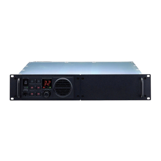
Rack mount repeater
Hide thumbs
Also See for VXR-9000:
- Service manual (118 pages) ,
- Operating manual (17 pages) ,
- Specifications (4 pages)
Table of Contents
Advertisement
Quick Links
Rack Mount Repeater
VXR-9000
Service Manual
©
2006 VERTEX STANDARD CO., LTD.
This manual provides the technical information necessary for servicing the VXR-9000 Rack Mount Repeater.
Servicing this equipment requires expertise in handing surface-mount chip components. Attempts by non-qualified
persons to service this equipment may result in permanent damage not covered by the warranty, and may be illegal
in some countries.
Two PCB layout diagrams are provided for each double-sided board in this transceiver. Each side of the board is
referred to by the type of the majority of components installed on that side ("Side A" or "Side B"). In most cases one
side has only chip components (surface-mount devices), and the other has either a mixture of both chip and leaded
components (trimmers, coils, electrolytic capacitors, ICs, etc.), or leaded components only.
As described in the pages to follow, the advanced microprocessor design of the VXR-9000 allows a complete align-
ment of this transceiver to be performed without opening the case of the radio; all adjustments can be performed from
the personal computer, using with the Vertex Standard VPL-1 Programming Cable and CE60 Software.
While we believe the information in this manual to be correct, Vertex Standard assumes no liability for damage that
may occur as a result of typographical or other errors that may be present. Your cooperation in pointing out any
inconsistencies in the technical information would be appreciated.
Specifications ........................................................... A-1
DSUB 25-pin Accessory Connector ...................... B-1
Block Diagram ......................................................... D-1
Connection Diagram ............................................... E-1
Circuit Description .................................................. F-1
Alignment ................................................................ G-1
UHF
EC044U90B
Contents
Board Units (Schematics, Layouts & Parts)
VERTEX STANDARD CO., LTD.
4-8-8 Nakameguro, Meguro-Ku, Tokyo 153-8644, Japan
VERTEX STANDARD
US Headquarters
10900 Walker Street, Cypress, CA 90630, U.S.A.
YAESU EUROPE B.V.
P.O. Box 75525, 1118 ZN Schiphol, The Netherlands
YAESU UK LTD.
Unit 12, Sun Valley Business Park, Winnall Close
Winchester, Hampshire, SO23 0LB, U.K.
VERTEX STANDARD HK LTD.
Unit 5, 20/F., Seaview Centre, 139-141 Hoi Bun Road,
Kwun Tong, Kowloon, Hong Kong
MAIN Unit .......................................................... H-1
CNTL Unit ............................................................ I-1
PANEL Unit .......................................................... J-1
PA Unit ................................................................. K-1
PA-2 Unit .............................................................. L-1
REG Unit ............................................................. M-1
SUB Unit .............................................................. N-1
100 W PA Unit (Option: Version D) ................. O-1
RELAY Unit (Option) ......................................... P-1
Advertisement
Table of Contents

Related Manuals for Vertex Standard VXR-9000


Summary of Contents for Vertex Standard VXR-9000
-
Page 1: Table Of Contents
(trimmers, coils, electrolytic capacitors, ICs, etc.), or leaded components only. As described in the pages to follow, the advanced microprocessor design of the VXR-9000 allows a complete align- ment of this transceiver to be performed without opening the case of the radio; all adjustments can be performed from the personal computer, using with the Vertex Standard VPL-1 Programming Cable and CE60 Software. -
Page 2: Specifications
Specifications General Frequency Range: A : 400 - 430 MHz, D : 450 - 490 MHz, F : 480 - 512 MHz Number of channel: Channel Spacing: 5 kHz/6.25 kHz Operating Voltage: 13.6 V DC ±10 % Current Drain: 12 A Maximum Duty Cycle: Receive : 100 % Transmit : 100 % (@25 W output) -
Page 3: Dsub 25-Pin Accessory Connector
DSUB 25-pin Accessory Connector Pin 5: TX ATT The VXR-9000 repeater is provided with a 25-pin DB-25F female connector for interconnections to accessories.Use This output is intended for controlling an external coaxial a DB-25M 25-pin male connector to connect accessories switching relay. - Page 4 UTPUT FOR OMMUNICATIONS ( 300 ~ 3,000 Hz ) The VXR-9000 provides eight ports (PIO) that can be pro- This pin is an output for low speed receiving data signals grammed for various input or output signals, or for con- (typically 1200 bps), with the data being extracted after trol functions.
- Page 5 DSUB 25-pin Accessory Connector I/O P ROGRAMMABLE NPUT TEMS Item Function Item Function Bin _ CH _ 0 Monitor _ On Recall the Memory Channel (Binary LSB) Turn the Monitor Function "On" Bin _ CH _ 1 Monitor _ Off Recall the Memory Channel (Binary) Turn the Monitor Function "Off"...
- Page 6 DSUB 25-pin Accessory Connector Note:...
-
Page 7: Exploded View & Miscellaneous Parts
Exploded View & Miscellaneous Parts RA0505300 REF. VXSTD P/N DESCRIPTION QTY. TOP CASE U00508001 PAN HEAD SCREW M5X8 U30408007 FLAT HEAD SCREW M4X8B U51416007 HEXA SOCKET BOLT M4X16B U20208002 BINDING HEAD SCREW M2.6X8NI U20406002 BINDING HEAD SCREW M4X6NI U20410002 BINDING HEAD SCREW M4X10NI U04408001 SEMS SCREW HSM4X8 RA03328A0... - Page 8 Exploded View & Miscellaneous Parts...
-
Page 9: Block Diagram
Block Diagam MAIN Unit... - Page 10 Block Diagam CNTL Unit, PANEL Unit, & PA Unit...
-
Page 11: Connection Diagram
Connection Diagam... - Page 12 Connection Diagam (with Optional 100 W PA Unit)
-
Page 13: Circuit Description
Circuit Description ume control Q1056 (M51132FP), where the maximum de- ECEIVE IGNAL viation is set. The audio signal subsequently passes Incoming RF from the RX antenna jack is delivered to the through the 3-section active low pass filter consisting of MAIN Unit and passes through the protection diode Q1017-1/-2/-3 (NJM2902V) and audio amplifier Q1001 D1001 (1SS302) and a varactor-tuned band pass filter con-... - Page 14 Circuit Description (HD64F2238) on the CNTL Unit, which compares the Changes in the DC voltage applied to the varactor diodes squelch threshold level to that which is memorized in EE- D1018/D1019 and D1020/D1021 (all 1SV282) affect the PROM Q3006 (BR24L32F) or set by the front panel SQL reactance in the tank circuit RX VCO Q1048/1049 (both control.
- Page 15 Circuit Description Q5002 (2SB1122S), which regulates supply voltage to Q5001 (2SC3357). CNTL C ONTROL The CNTL Unit consists of 8-bit CPU Q3014 (HD64F2238), EEPROM Q3006 (BR24L32F), RX and TX speech audio circuits, and various analog switches for the CPU and re- peater interconnections.
- Page 16 Circuit Description Note:...
-
Page 17: Alignment
Alignment Introduction Required Test Equipment The VXR-9000 has been aligned at the factory for the spec- RF Signal Generator with calibrated output level at 1 ified performance across the entire frequency range spec- ified. Realignment should therefore not be necessary ex- AF Signal Generator cept in the event of a component failure. - Page 18 Modulation Balance Repeat Sensitivity TX Power Down Detect PLL Reference Frequency RX Sensitivity Setup the test equipment as shown below. EXT SP RF Signal VXR-9000 SINAD Meter RX ANT Generator 4-ohm Computer ( CE60 ) Dummy Load Open the “Alignment” window, then click the mouse button on the “Rx Tune”...
- Page 19 Press the [ Page Down ] key until the squelch close, then Setup the test equipment as shown below. press the [ Page Up ] key to the point where the squelch Computer RF Signal VXR-9000 is just opened. ( CE60 ) Generator RX ANT Repeat the above steps at the four points (box: frequen- Open the “Alignment”...
- Page 20 (the “PTT Off” label is re- Sampling Coupler turned to “PTT On”). 50-ohm VXR-9000 Dummy Load Repeat the above steps at the “Narrow” box on the TX ANT “Low Band Edge Frequency” area of the “MAX De- viation (Audio)”...
- Page 21 Band Edge Frequency” area of the “MAX Deviation Sampling Coupler (CTCSS/DCS)” field (highlighted in “pink”) so that the 50-ohm VXR-9000 Deviation Meter reading is 0.38 kHz ±0.08 kHz. Dummy Load TX ANT Repeat the above steps at the eight points (box: fre- quencies).
- Page 22 Meter reading is 3.0 kHz ±0.2 kHz. Sampling Coupler Click the left mouse button on the “Repeat TX Off” 50-ohm Computer VXR-9000 ( CE60 ) Dummy Load button to disable the transmitter (the “Repeat TX Off” TX ANT label is returned to “Repeat Sens. Enb”).
- Page 23 Counter reading is “Low Band Edge Fre- needs to add a “Chip Resistor” on to the Main Unit. For fur- quency” ±100 Hz. ther details contact to Vertex Standard. Click the left mouse button on the “PTT Off” button Setup the test equipment as shown below.
- Page 24 Alignment Note:...
- Page 25 MAIN Unit (Lot. 1~2) Circuit Diagram (8.0 V) 4.9 V 8.9 V (8.4 V) Frequency: 470.20 MHz 8.9 V (468.80 MHz) 8.0 V 2.2 V 2.2 V 1.3 V (4.2 V) 2.3 V 0.9 V 2.2 V 2.2 V 7.1 V 1.5 V WIDE: 0.1 V NARROW: 7.5 V...
- Page 26 MAIN Unit (Lot. 1~2) Note...
- Page 27 MAIN Unit (Lot. 1~2) Parts Layout (Side A) M51132FP NJM2902V (Q1006, 1056) (Q1001, 1017, 1025) MB15A02PFV1 (Q1008, 1052) TA31136FN (Q1028) NJM2904V TDA2003 (Q1004, 1020, 1050) (Q1057) 2SK508 (K52) 2SA1586Y (SY) (Q1021, 1048, (Q1051) 1049) 2SC3357 (RK) SPM5001 (Q1009, 1030) (Q1018) 2SC4116GR (LG) (Q1007, 1033, 1045, 1046, 1061)
- Page 28 MAIN Unit (Lot. 1~2) Parts Layout (Side B) L78M05T M62364FP BU4066BCFV (Q1062) (Q1055) (Q1040) NJM2904V 2SA1162GR (SG) 2SB1122S (BE) (Q1010) (Q1014, 1041) (Q1029) 2SA1179 (M6) (Q1034) 2SA1586Y (SY) (Q1012) 2SC3357 (RK) 2SC2712GR (LG) DTA144EE (16) (Q1019) (Q1015, 1042) (Q1037) 2SD1664 (DA) 2SC2812 (LG) (Q1002) (Q1023)
- Page 29 MAIN Unit (Lot. 3~24) Circuit Diagram...
- Page 30 MAIN Unit (Lot. 3~24) Note...
- Page 31 MAIN Unit (Lot. 3~24) Parts Layout (Side A) M51132FP NJM2902V (Q1006, 1056) (Q1001, 1017, 1025) MB15A02PFV1 (Q1008, 1052) TA31136FN (Q1028) NJM2904V TDA2003 (Q1004, 1020, 1050) (Q1057) 2SK508 (K52) 2SA1586Y (SY) (Q1021, 1048, (Q1051) 1049) 2SC3357 (RK) SPM5001 (Q1009, 1030) (Q1018) 2SC4116GR (LG) (Q1007, 1033, 1045, 1046, 1061)
- Page 32 MAIN Unit (Lot. 3~24) Parts Layout (Side B) L78M05T M62364FP BU4066BCFV (Q1062) (Q1055) (Q1040) NJM2904V 2SA1162GR (SG) 2SB1122S (BE) (Q1010) (Q1014, 1041) (Q1029) 2SA1179 (M6) (Q1034) 2SA1586Y (SY) (Q1012) 2SC3357 (RK) 2SC2712GR (LG) DTA144EE (16) (Q1019) (Q1015, 1042) (Q1037) 2SD1664 (DA) 2SC2812 (LG) (Q1002) (Q1023)
- Page 33 MAIN Unit (Lot. 25~) Circuit Diagram...
- Page 34 MAIN Unit (Lot. 25~) Note H-10...
- Page 35 MAIN Unit (Lot. 25~) Parts Layout (Side A) M51132FP NJM2902V (Q1006, 1056) (Q1001, 1017, 1025) MB15A02PFV1 (Q1008, 1052) TA31136FN (Q1028) NJM2904V TDA2003 (Q1004, 1020, 1050) (Q1057) 2SK508 (K52) 2SA1586Y (SY) (Q1021, 1048, (Q1051) 1049) 2SC3357 (RK) SPM5001 (Q1009, 1030) (Q1018) 2SC4116GR (LG) (Q1007, 1033, 1045, 1046, 1061)
- Page 36 MAIN Unit (Lot. 25~) Parts Layout (Side B) L78M05T M62364FP BU4066BCFV (Q1062) (Q1055) (Q1040) NJM2904V 2SA1162GR (SG) 2SB1122S (BE) (Q1010) (Q1014, 1041) (Q1029) 2SA1179 (M6) (Q1034) 2SA1586Y (SY) (Q1012) 2SC3357 (RK) 2SC2712GR (LG) DTA144EE (16) (Q1019) (Q1015, 1042) (Q1037) 2SD1664 (DA) 2SC2812 (LG) (Q1002) (Q1023)
-
Page 37: Main Unit
MAIN Unit Parts List Parts List DESCRIPTION VALUE TOL. MFR'S DESIG VXSTD P/N VERS. SIDE LAY ADR PCB with Components CB2115001 VER. D CB2115002 VER. CS CB2115003 VER. A Printed Circuit Board. AC044U000 FR008640B AC044U000 FR008640C 3-22 AC044U000 FR014710A VER. A 23-24 AC044U000 FR008640C... - Page 38 MAIN Unit Parts List DESCRIPTION VALUE TOL. MFR'S DESIG VXSTD P/N VERS. SIDE LAY ADR C 1075 CHIP CAP. GRM1882C1H7R0DZ01D K22174208 1-20 C 1075 CHIP CAP. GRM1882C1H8R0CZ01D K22174246 VER. A C 1075 CHIP CAP. GRM1882C1H7R0DZ01D K22174208 VER. CS 21- C 1075 CHIP CAP.
- Page 39 MAIN Unit Parts List DESCRIPTION VALUE TOL. MFR'S DESIG VXSTD P/N VERS. SIDE LAY ADR C 1153 CHIP CAP. 0.001uF GRM188B11H102KA01D K22174821 C 1154 CHIP CAP. GRM1884C1H1R0CZ01D K22174202 1-20 C 1154 CHIP CAP. GRM1884C1H2R0CZ01D K22174203 VER. A C 1154 CHIP CAP. GRM1884C1H2R0CZ01D K22174203 VER.
- Page 40 MAIN Unit Parts List DESCRIPTION VALUE TOL. MFR'S DESIG VXSTD P/N VERS. SIDE LAY ADR C 1215 CHIP CAP. 56pF GRM1882C1H560JA01D K22174229 C 1216 CHIP CAP. 0.001uF GRM188B11H102KA01D K22174821 C 1218 CHIP CAP. 0.1uF GRM188B11C104KA01D K22124805 C 1219 CHIP CAP. 0.1uF GRM188B11C104KA01D K22124805...
- Page 41 MAIN Unit Parts List DESCRIPTION VALUE TOL. MFR'S DESIG VXSTD P/N VERS. SIDE LAY ADR C 1278 CHIP CAP. GRM1882C1H9R0DZ01D K22174210 VER. D C 1281 CHIP CAP. 0.001uF GRM188B11H102KA01D K22174821 C 1282 CHIP CAP. 0.001uF GRM188B11H102KA01D K22174821 C 1283 CHIP CAP. GRM1883C1H3R0CZ01D K22174204 VER.
- Page 42 MAIN Unit Parts List DESCRIPTION VALUE TOL. MFR'S DESIG VXSTD P/N VERS. SIDE LAY ADR C 1335 CHIP CAP. 0.001uF GRM188B11H102KA01D K22174821 C 1336 CHIP CAP. 0.001uF GRM188B11H102KA01D K22174821 C 1337 CHIP CAP. 0.01uF GRM188B11H103KA01D K22174823 C 1338 CHIP CAP. 0.001uF GRM188B11H102KA01D K22174821...
- Page 43 MAIN Unit Parts List DESCRIPTION VALUE TOL. MFR'S DESIG VXSTD P/N VERS. SIDE LAY ADR C 1398 CHIP CAP. 0.5pF GRM1884C1HR50CZ01D K22174201 3-20 C 1398 CHIP CAP. GRM1884C1H1R0CZ01D K22174202 VER. A C 1398 CHIP CAP. 0.5pF GRM1884C1HR50CZ01D K22174201 VER. CS 21-25 A C 1398 CHIP CAP.
- Page 44 MAIN Unit Parts List DESCRIPTION VALUE TOL. MFR'S DESIG VXSTD P/N VERS. SIDE LAY ADR C 1515 CHIP CAP. GRM1882C1H8R0DZ01D K22174209 C 1517 CHIP CAP. GRM1882C1H8R0DZ01D K22174209 C 1518 CHIP CAP. 0.01uF GRM188B11H103KA01D K22174823 C 1520 CHIP CAP. 0.001uF GRM188B11H102KA01D K22174821 C 1521 CHIP CAP.
- Page 45 MAIN Unit Parts List DESCRIPTION VALUE TOL. MFR'S DESIG VXSTD P/N VERS. SIDE LAY ADR L 1005 M.RFC 0.015uH LL1608-F15NK L1690361 L 1006 M.RFC 4.7uH LK1608 4R7K-T L1690688 L 1007 M.RFC 3.3uH LK1608 3R3K-T L1690686 L 1008 CHIP COIL 0.017uH LQW31HN17NJ03L L1690249 L 1009...
- Page 46 MAIN Unit Parts List DESCRIPTION VALUE TOL. MFR'S DESIG VXSTD P/N VERS. SIDE LAY ADR L 1451 M.RFC 0.027uH HK1608 27NJ-T L1690521 VER. A L 1452 M.RFC 0.027uH HK1608 27NJ-T L1690521 VER. A L 1453 M.RFC 0.027uH HK1608 27NJ-T L1690521 VER.
- Page 47 MAIN Unit Parts List DESCRIPTION VALUE TOL. MFR'S DESIG VXSTD P/N VERS. SIDE LAY ADR Q 1052 MB15A02PFV1-G-BND-EFE1 G1092541 Q 1053 TRANSISTOR DTC144EE TL G3070075 Q 1053 TRANSISTOR RT1N441U-T11-1 G3070247 VER. A Q 1053 TRANSISTOR RT1N441U-T11-1 G3070247 VER. CS 4- Q 1053 TRANSISTOR DTC144EE TL...
- Page 48 MAIN Unit Parts List DESCRIPTION VALUE TOL. MFR'S DESIG VXSTD P/N VERS. SIDE LAY ADR R 1050 CHIP RES. 150k 1/16W RMC1/16 154JATP J24185154 VER. A R 1050 CHIP RES. 100k 1/16W RMC1/16 104JATP J24185104 VER. CS 23- R 1050 CHIP RES.
- Page 49 MAIN Unit Parts List DESCRIPTION VALUE TOL. MFR'S DESIG VXSTD P/N VERS. SIDE LAY ADR R 1119 CHIP RES. 1/16W RMC1/16 000JATP J24185000 R 1119 CHIP RES. 6.8k 1/16W RMC1/16 682JATP J24185682 R 1119 CHIP RES. 1/16W RMC1/16 103JATP J24185103 R 1121 CHIP RES.
- Page 50 MAIN Unit Parts List DESCRIPTION VALUE TOL. MFR'S DESIG VXSTD P/N VERS. SIDE LAY ADR R 1187 CHIP RES. 4.7k 1/16W RMC1/16 472JATP J24185472 R 1188 CHIP RES. 1/16W RMC1/16 100JATP J24185100 R 1189 CHIP RES. 1/16W RMC1/16 103JATP J24185103 R 1190 CHIP RES.
- Page 51 MAIN Unit Parts List DESCRIPTION VALUE TOL. MFR'S DESIG VXSTD P/N VERS. SIDE LAY ADR R 1251 CHIP RES. 1/16W RMC1/16 331JATP J24185331 VER. CS 21- R 1251 CHIP RES. 1/16W RMC1/16 331JATP J24185331 VER. CS 23- R 1251 CHIP RES. 1/16W RMC1/16 331JATP J24185331...
- Page 52 MAIN Unit Parts List DESCRIPTION VALUE TOL. MFR'S DESIG VXSTD P/N VERS. SIDE LAY ADR R 1324 CHIP RES. 1/16W RMC1/16 100JATP J24185100 R 1325 CHIP RES. 2.2k 1/16W RMC1/16 222JATP J24185222 R 1326 CHIP RES. 1/16W RMC1/16 180JATP J24185180 R 1327 CHIP RES.
- Page 53 MAIN Unit Parts List DESCRIPTION VALUE TOL. MFR'S DESIG VXSTD P/N VERS. SIDE LAY ADR R 1518 CHIP RES. 1/16W RMC1/16 391JATP J24185391 VER. A 23-24 B R 1518 CHIP RES. 1/16W RMC1/16 391JATP J24185391 R 1519 CHIP RES. 1/16W RMC1/16 000JATP J24185000 R 1519...
- Page 54 MAIN Unit Parts List Note DESCRIPTION VALUE TOL. MFR'S DESIG VXSTD P/N VERS. SIDE LAY ADR H-30...
- Page 55 CNTL Unit Circuit Diagram...
- Page 56 CNTL Unit Note...
- Page 57 CNTL Unit Parts Layout (Side A) 2SB1201S LA8630M BU4066BCFV NJM12903R NJM2904V 2SC4116GR (LG) DTA144EE (16) DTC124TE (25) DTC144EE (26) DTC323TK (H02) FMG2 (G2) TA75S01F (SA) (Q3004, 3055) (Q3034) (Q3030, 3032, 3033) (Q3043) (Q3035, 3041) (Q3025) (Q3026) (Q3031) (Q3028, 3029, 3037, (Q3015) (Q3024) (Q3016, 3036, 3059)
- Page 58 CNTL Unit Parts Layout (Side B) FX805LG 2SA1586Y (SY) 2SC4116GR (LG) 3SK3065 (LG) AN8005M (LG) BD4845FVE DTC144EE (26) DTC323TK (H02) FMG2 (G2) TA75S01F (SA) TC7S66FU (E9) (Q3020) (Q3022, 3054) (Q3017, 3018) (Q3005, 3009) (Q3007) (Q3012) (Q3046, 3052, 3053) (Q3038) (Q3010, 3011, 3039) (Q3002, 3019, 3023) (Q3051) HD64F2238BFA...
-
Page 59: Cntl Unit
CNTL Unit Parts List Parts List DESCRIPTION VALUE TOL. MFR'S DESIG VXSTD P/N VERS. SIDE LAY ADR PCB with Components CS1843001 VER. VTX D CS1843002 VER. EXP D CS1843003 VER. EXP CS CS1843004 VER. AUS D CS1843005 VER. VTX A CS1843006 VER. - Page 60 CNTL Unit Parts List DESCRIPTION VALUE TOL. MFR'S DESIG VXSTD P/N VERS. SIDE LAY ADR C 3067 CHIP CAP. 0.01uF GRM188B11H103KA01D K22174823 C 3068 CHIP CAP. 15pF GRM1882C1H150JA01D K22174215 C 3069 CHIP CAP. 15pF GRM1882C1H150JA01D K22174215 C 3071 CHIP TA.CAP. 4.7uF TEMSVA1C475M-8R K78120031...
- Page 61 CNTL Unit Parts List DESCRIPTION VALUE TOL. MFR'S DESIG VXSTD P/N VERS. SIDE LAY ADR C 3140 CHIP CAP. 82pF GRM1882C1H820JA01D K22174233 C 3141 CHIP TA.CAP. 2.2uF TESVA1A225M1-8R K78100021 C 3142 CHIP TA.CAP. 4.7uF TEMSVA1C475M-8R K78120031 C 3144 CHIP CAP. 560pF GRM39CH561J25PT K22144201...
- Page 62 CNTL Unit Parts List DESCRIPTION VALUE TOL. MFR'S DESIG VXSTD P/N VERS. SIDE LAY ADR C 3224 CHIP CAP. 0.01uF GRM188B11H103KA01D K22174823 C 3225 CHIP TA.CAP. TEMSVA1E105M-8R K78140013 C 3226 CHIP TA.CAP. TEMSVA1E105M-8R K78140013 C 3227 CHIP TA.CAP. TEMSVA1E105M-8R K78140013 C 3228 CHIP CAP.
- Page 63 R 3004 CHIP RES. 180k 1/16W RMC1/16 184JATP J24185184 1-22 R 3004 CHIP RES. 1/16W RMC1/16 223JATP J24185223 R 3004 CHIP RES. 180k 1/16W RMC1/16 184JATP J24185184 R 3004 CHIP RES. 1/16W RMC1/16 223JATP J24185223 : Please contact Vertex Standard I-13...
- Page 64 CNTL Unit Parts List DESCRIPTION VALUE TOL. MFR'S DESIG VXSTD P/N VERS. SIDE LAY ADR R 3005 CHIP RES. 1/16W RMC1/16 473JATP J24185473 R 3006 CHIP RES. 1/16W RMC1/16 683JATP J24185683 R 3007 CHIP RES. 1/16W RMC1/16 153JATP J24185153 R 3008 CHIP RES.
- Page 65 CNTL Unit Parts List DESCRIPTION VALUE TOL. MFR'S DESIG VXSTD P/N VERS. SIDE LAY ADR R 3082 CHIP RES. 1/16W RMC1/16 000JATP J24185000 R 3084 CHIP RES. 6.8k 1/16W RMC1/16 682JATP J24185682 R 3085 CHIP RES. 150k 1/16W RMC1/16 154JATP J24185154 R 3086 CHIP RES.
- Page 66 CNTL Unit Parts List DESCRIPTION VALUE TOL. MFR'S DESIG VXSTD P/N VERS. SIDE LAY ADR R 3166 CHIP RES. 1/16W RMC1/16 000JATP J24185000 R 3168 CHIP RES. 1/16W RMC1/16 153JATP J24185153 R 3169 CHIP RES. 1/16W RMC1/16 103JATP J24185103 R 3170 CHIP RES.
- Page 67 CNTL Unit Parts List DESCRIPTION VALUE TOL. MFR'S DESIG VXSTD P/N VERS. SIDE LAY ADR R 3250 CHIP RES. 4.7k 1/16W RMC1/16 472JATP J24185472 R 3251 CHIP RES. 1/16W RMC1/16 103JATP J24185103 R 3252 CHIP RES. 1/16W RMC1/16 102JATP J24185102 R 3253 CHIP RES.
- Page 68 CNTL Unit Parts List Note DESCRIPTION VALUE TOL. MFR'S DESIG VXSTD P/N VERS. SIDE LAY ADR I-18...
- Page 69 PANEL Unit Circuit Diagram...
- Page 70 PANEL Unit Note...
- Page 71 PANEL Unit Parts Layout (Side A) RT1P441U (P3) MC2850 (A7) (Q4006) (D4002)
- Page 72 PANEL Unit Parts Layout (Side B) BU4094BCFV BU4066BCFV DTC144EE (26) DTC323TK (H02) XN1213 (9L) MC2850 (A7) (Q4003, 4011, 4014) (Q4008) (Q4004, 4012) (Q4002) (Q4005, 4007, 4009, (D4006, 4011, 4013, 4010, 4013, 4015, 4015, 4016, 4019) NJM2902V DTC144EK (26) 4016, 4017, 4018, (Q4001) (Q1043) 4019, 4020, 4021,...
- Page 73 PANEL Unit Parts List DESCRIPTION VALUE TOL. MFR'S DESIG VXSTD P/N VERS. SIDE LAY ADR PCB with Components CB2328001 Printed Circuit Board AC044U000 FR009570D C 4001 CHIP TA.CAP. 4.7uF TEMSVA1C475M-8R K78120031 C 4002 CHIP CAP. 0.001uF GRM188B11H102KA01D K22174821 C 4003 CHIP CAP.
- Page 74 PANEL Unit Parts List DESCRIPTION VALUE TOL. MFR'S DESIG VXSTD P/N VERS. SIDE LAY ADR Q 4005 TRANSISTOR XN1213-(TX) G3070194 Q 4006 TRANSISTOR RT1P441U-T11-1 G3070248 Q 4007 TRANSISTOR XN1213-(TX) G3070194 Q 4008 BU4066BCFV-E2 G1093537 Q 4009 TRANSISTOR XN1213-(TX) G3070194 Q 4010 TRANSISTOR XN1213-(TX) G3070194...
-
Page 75: Panel Unit
PANEL Unit Parts List DESCRIPTION VALUE TOL. MFR'S DESIG VXSTD P/N VERS. SIDE LAY ADR R 4057 CHIP RES. 1/16W RMC1/16 473JATP J24185473 R 4058 CHIP RES. 1/4W RMC1/4 561JATP J24245561 R 4059 CHIP RES. 1/16W RMC1/16 103JATP J24185103 R 4060 CHIP RES. - Page 76 PANEL Unit Parts List Note: DESCRIPTION VALUE TOL. MFR'S DESIG VXSTD P/N VERS. SIDE LAY ADR...
- Page 77 PA Unit (Lot. 1~2) Circuit Diagram...
- Page 78 PA Unit (Lot. 1~2) Note:...
- Page 79 PA Unit (Lot. 1~2) Parts Layout (Side A) PD55008 (Q5008) PD55025S (Q5015, 5016) 2SB1122S (BE) 2SB1132 (BA) (Q5002) (Q5007) 2SC2812 (L6) DTC144EE (26) (Q5010) (Q5006, 5009, 5011) 2SC3357 (RK) (Q5001) 2SC4116GR (LG) (Q5004) 2SC4154 (LE) (Q5014) TA75S01F (SA) NJM78L09 (8H) (Q5005) (Q5003) TC4S66F (C9)
- Page 80 PA Unit (Lot. 1~2) Parts Layout (Side B)
- Page 81 PA Unit (Lot. 3~20) Circuit Diagram...
- Page 82 PA Unit (Lot. 3~20) Note:...
- Page 83 PA Unit (Lot. 3~20) Parts Layout (Side A) PD55008 (Q5008) PD55025S (Q5015, 5016) 2SB1122S (BE) 2SB1132 (BA) (Q5002) (Q5007) 2SC2812 (L6) DTC144EE (26) (Q5010) (Q5006, 5009, 5011) 2SC3357 (RK) (Q5001) 2SC4116GR (LG) (Q5004) 2SC4154 (LE) (Q5014) TA75S01F (SA) NJM78L09 (8H) (Q5005) (Q5003) TC4S66F (C9)
- Page 84 PA Unit (Lot. 3~20) Parts Layout (Side B)
- Page 85 PA Unit (Lot. 1~20) Parts List DESCRIPTION VALUE TOL. MFR'S DESIG VXSTD P/N VERS. SIDE LAY ADR PCB with Components CS1813001 Printed Circuit Board AC044U000 FR008660B FR008660C C 5001 CHIP CAP. 0.001uF GRM188B11H102KA01D K22174821 C 5002 CHIP CAP. 0.001uF GRM188B11H102KA01D K22174821 C 5003 CHIP CAP.
- Page 86 PA Unit (Lot. 1~20) Parts List DESCRIPTION VALUE TOL. MFR'S DESIG VXSTD P/N VERS. SIDE LAY ADR C 5075 FILM CAP. 27pF 500V UC232H0270J-T K33279023 C 5076 CHIP CAP. 0.01uF GRM188B11H103KA01D K22174823 C 5077 CHIP CAP. 0.001uF ECUV1H102KBN K22179550 C 5078 FILM CAP.
-
Page 87: Pa Unit
PA Unit (Lot. 1~20) Parts List DESCRIPTION VALUE TOL. MFR'S DESIG VXSTD P/N VERS. SIDE LAY ADR FB5008 FERRITE BEADS 4A2 RI3X3-1 L9190001 FB5009 FERRITE BEADS 4A2 RI3X3-1 L9190001 FB5010 FERRITE BEADS 4A2 RI3X3-1 L9190001 FB5011 FERRITE BEADS 4A2 RI3X3-1 L9190001 FB5012 FERRITE BEADS... - Page 88 PA Unit (Lot. 1~20) Parts List DESCRIPTION VALUE TOL. MFR'S DESIG VXSTD P/N VERS. SIDE LAY ADR R 5034 CHIP RES. 1/16W RMC1/16 000JATP J24185000 R 5035 CHIP RES. 1/16W RMC1/16 333JATP J24185333 R 5036 CHIP RES. 1/16W RMC1/16 333JATP J24185333 R 5037 CHIP RES.
-
Page 89: Pa-2 Unit
PA-2 Unit (Lot. 21~) Circuit Diagram... - Page 90 PA-2 Unit (Lot. 21~) Note:...
- Page 91 PA-2 Unit (Lot. 21~) Parts Layout (Side A) S-AU82L LM2904PWR (Q8007) (Q8018) S-AU93 (Q8007) 2SA1179 (M6) 2SB1132 (BA) (Q8004) (Q5007) 2SC2812 (L6) DTC144EE (26) (Q8008) (Q8002, 8005) 2SC5415E (EA) (Q8003) FMG2 (G2) NJM78L09 (8H) (Q8006) (Q8001) HSM88AS HZM4.7NB2 (472) (D8006, 8007) (D8004) RN739F (5F) HZM9.1NB2 (912)
- Page 92 PA-2 Unit (Lot. 21~) Parts Layout (Side B)
- Page 93 PA-2 Unit (Lot. 21~) Parts List DESCRIPTION VALUE TOL. MFR'S DESIG VXSTD P/N VERS. SIDE LAY ADR PCB with Components CB3195001 VER. A CB3195002 VER. D Printed Circuit Board AC044U000 FR013570B C 8001 CHIP CAP. 100pF GRM1882C1H101JA01D K22174235 C 8002 CHIP CAP.
- Page 94 PA-2 Unit (Lot. 21~) Parts List DESCRIPTION VALUE TOL. MFR'S DESIG VXSTD P/N VERS. SIDE LAY ADR D 8007 DIODE HSM88AS TR G2070170 D 8008 DIODE BAS316 G2070716 D 8009 DIODE HZM9.1NB3TR G2070404 D 8010 DIODE BAS316 G2070716 D 8011 SURGE ABSORBER P6KA18 Q9000721...
- Page 95 PA-2 Unit (Lot. 21~) Parts List DESCRIPTION VALUE TOL. MFR'S DESIG VXSTD P/N VERS. SIDE LAY ADR R 8038 CHIP RES. 22kohm 1/16W RMC1/16 223JATP J24185223 R 8039 CHIP RES. 22ohm 1/10W RMC1/10T 220J J24205220 R 8040 CHIP RES. 47kohm 1/16W RMC1/16 473JATP J24185473...
- Page 96 PA-2 Unit (Lot. 21~) Parts List Note DESCRIPTION VALUE TOL. MFR'S DESIG VXSTD P/N VERS. SIDE LAY ADR...
-
Page 97: Reg Unit
REG Unit Circuit Diagram... - Page 98 REG Unit Parts Layout KIA7809API (Q3901, 3902) Side A Side B Parts List DESCRIPTION VALUE TOL. MFR'S DESIG VXSTD P/N VERS. SIDE LAY ADR PCB with Components CB2565001 Printed Circuit Board AC044U000 FR0108700 C 3901 CHIP TA.CAP. 4.7uF TEMSVA1C475M-8R K78120031 C 3902 CHIP CAP.
-
Page 99: Sub Unit
SUB Unit (Lot. 1~2) Circuit Diagram... - Page 100 SUB Unit (Lot. 1~2) Parts Layout Side A Side B FMG2 (G2) MC2848 (A6) (Q3802, 3803) (D3801) TC4S81F (C2) TC4S66F (C9) (Q3801) (Q3804) Parts List DESCRIPTION VALUE TOL. MFR'S DESIG VXSTD P/N VERS. SIDE LAY ADR PCB with Components CB2672001 Printed Circuit Board AC044U000 FR011450A...
- Page 101 100W PA Unit (Option: Version D) Circuit Diagram...
- Page 102 100W PA Unit (Option: Version D) Note...
- Page 103 100W PA Unit (Option: Version D) Parts Layout (Side A) S-AU82L (Ver. A) (Q6011, 6014) S-AU93 (Ver. D) (Q6011, 6014) LM2904 LM2902 (Q6013) (Q6012) 2SA812 (M7) 2SC5415E (EA) (Q6005, 6015, (Q6004) 6016) FMG2 (G2) DTC144EE (26) (Q6002, 6009, (Q6002, 6009, 6010) 6010) NJM78L09 (8H)
- Page 104 100W PA Unit (Option: Version D) Parts Layout (Side B)
- Page 105 100W PA Unit (Option: Version D) Parts List DESCRIPTION VALUE TOL. MFR'S DESIG VXSTD P/N VERS. SIDE LAY ADR PCB with Components CS1866001 VER. D Printed Circuit Board AAE21U000 FR0134100 C 6001 CHIP CAP. 100pF GRM1882C1H101JA01D K22174235 C 6002 CHIP CAP. 100pF GRM1882C1H101JA01D K22174235...
- Page 106 100W PA Unit (Option: Version D) Parts List DESCRIPTION VALUE TOL. MFR'S DESIG VXSTD P/N VERS. SIDE LAY ADR C 6088 CHIP CAP. 10pF GRM1882C1H100JA01D K22174211 C 6089 CHIP CAP. 10pF GRM1882C1H100JA01D K22174211 C 6090 CHIP CAP. 10pF GRM1882C1H100JA01D K22174211 C 6091 CHIP CAP.
-
Page 107: Pa Unit (Option: Version D
100W PA Unit (Option: Version D) Parts List DESCRIPTION VALUE TOL. MFR'S DESIG VXSTD P/N VERS. SIDE LAY ADR R 6004 CHIP RES. 1/16W RMC1/16 271JATP J24185271 R 6005 CHIP RES. 1/16W RMC1/16 271JATP J24185271 R 6006 CHIP RES. 1/16W RMC1/16 180JATP J24185180 R 6007... - Page 108 100W PA Unit (Option: Version D) Parts List DESCRIPTION VALUE TOL. MFR'S DESIG VXSTD P/N VERS. SIDE LAY ADR R 6080 CHIP RES. 1/16W RMC1/16 102JATP J24185102 R 6082 CHIP RES. 1/16W RMC1/16 102JATP J24185102 R 6083 CHIP RES. 1/16W RMC1/16 102JATP J24185102 R 6084...
-
Page 109: Relay Unit (Option
RELAY Unit (Option) Circuit Diagram... - Page 110 RELAY Unit (Option) Parts Layout LM2902 2SB1201S (Q8003) (Q8007) 2SD1664 (DA) FMG2 (G2) DTC144EE (26) (Q8002, 8006) (Q8005) (Q8001, 8004, 8008) HZM9.1NB3 (913) C30T04QH (D6006) (D8002, 8003) Side A Side B...
- Page 111 RELAY Unit (Option) Parts List DESCRIPTION VALUE TOL. MFR'S DESIG VXSTD P/N VERS. SIDE LAY ADR PCB with Components CS1867001 Printed Circuit Board AAE21U000 FR0144000 C 8001 CHIP CAP. 100pF GRM1882C1H101JA01D K22174235 C 8002 CHIP CAP. 100pF GRM1882C1H101JA01D K22174235 C 8003 CHIP CAP.
- Page 112 RELAY Unit (Option) Parts List DESCRIPTION VALUE TOL. MFR'S DESIG VXSTD P/N VERS. SIDE LAY ADR D 8014 DIODE BAS316 G2070716 D 8015 DIODE UDZS TE-17 5.6B G2070910 F 8001 CHIP FUSE R429 001 Q0000089 F 8002 CHIP FUSE 451 015.MR 15A Q0000105 J 8001 TERMINAL...
- Page 114 Copyright 2006 VERTEX STANDARD CO., LTD. All rights reserved No portion of this manual may be reproduced without the permission of VERTEX STANDARD CO., LTD.