Table of Contents
Advertisement
Quick Links
Download this manual
See also:
Owner's Manual
CONTENTS(目次)
SPECIFICATIONS(総合仕様) ..................................3
PANEL LAYOUT(パネルレイアウト) .......................4
CIRCUIT BOARD LAYOUT(ユニットレイアウト) .....6
DIMENSIONS(寸法図) .............................................7
DISASSEMBLY PROCEDURE(分解手順) ...............8
LSI PIN DESCRIPTION(LSI 端子機能表) .............. 18
CIRCUIT BOARDS(シート基板図) ........................34
TEST PROGRAM(テストプログラム) ..............43/58
(ファームウェアのアップデート) ....................... 73/76
(DANTE モジュール(Brooklyn2)のアップデート) ...79/82
PA
012151
SERVICE MANUAL
SERVICE MANUAL
からの復帰方法) ......................................................85/87
INITIALIZATION(初期化) ..........................................89
FACTORY SET(出荷設定) .....................................90
START-UP SEQUENCE(起動シーケンス) ........91/92
ENDING SEQUENCE(終了シーケンス) ................93
BLOCK DIAGRAM(ブロックダイアグラム)
WIRING(結線図)
Copyright (c) Yamaha Corporation. All rights reserved. PDF
I/O RACK
HAMAMATSU, JAPAN
'15.10
Advertisement
Table of Contents

Related Manuals for Yamaha RSio64-D


Summary of Contents for Yamaha RSio64-D
-
Page 1: Table Of Contents
START-UP SEQUENCE(起動シーケンス) ..91/92 TEST PROGRAM(テストプログラム) ....43/58 ENDING SEQUENCE(終了シーケンス) ....93 UPDATING FIRMWARE PARTS LIST BLOCK DIAGRAM(ブロックダイアグラム) (ファームウェアのアップデート) ....... 73/76 UPDATING DANTE MODULE (Brooklyn2) WIRING(結線図) (DANTE モジュール(Brooklyn2)のアップデート) ...79/82 CIRCUIT DIAGRAM(回路図) 012151 HAMAMATSU, JAPAN Copyright (c) Yamaha Corporation. All rights reserved. PDF ’15.10... - Page 2 IMPORTANT NOTICE This manual has been provided for the use of authorized Yamaha Retailers and their service personnel. It has been assumed that basic service procedures inherent to the industry, and more specifically Yamaha Products, are already known and understood by the users, and have therefore not been restated.
-
Page 3: Specifications(総合仕様
RSio64-D SPECIFICATIONS(総合仕様) GENERAL SPECIFICATIONS (一般仕様) 44.1 kHz +4.1667 %/+0.1 %/-0.1 %/-4.0 % ±200 ppm ±200 ppm 48 kHz +4.1667 %/+0.1 %/-0.1 %/-4.0 % Sampling Frequency Frequency External Clock Range 88.2 kHz +4.1667 %/+0.1 %/-0.1 %/-4.0 % ±200 ppm 96 kHz +4.1667 %/+0.1 %/-0.1 %/-4.0 %... -
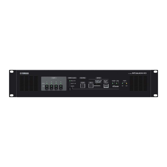
Page 4: Panel Layout(パネルレイアウト
RSio64-D PANEL LAYOUT(パネルレイアウト) • Front Panel (フロントパネル) 1 2 3 4 5 6 7 8 1 2 3 4 q SLOT 1–4 [LOCK] indicators q SLOT1 ∼ 4 [LOCK] インジケーター w SLOT 1–4 [SRC] indicators w SLOT1 ∼ 4 [SRC] インジケーター... - Page 5 RSio64-D • Rear Panel (リアパネル) Right side view (右側面) q [I]/[ ] (Power Switch) q [I]/[ ](電源スイッチ) w AC IN connector w AC IN 端子 e [EXT DC INPUT] connector e [EXT DC INPUT] 端子 r Grounding screw r アース用ネジ...
-
Page 6: Circuit Board Layout(ユニットレイアウト
RSio64-D CIRCUIT BOARD LAYOUT(ユニットレイアウト) <Rear view (背面) > PSW CONNECTOR ASSEMBLY (PSW 束線) INLET ASSEMBLY (インレット Ass’ y) DANTE MODULE 64CH <Top view (上面) > (ダンテモジュール 64CH) (SLOT1,3) (SLOT2,4) DC FAN MOTOR (DC ファンモーター) POWER SUPPLY UNIT (電源ユニット) FRONT PANEL ASSEMBLY (フロントパネル... -
Page 7: Dimensions(寸法図
RSio64-D DIMENSIONS(寸法図) 1 2 3 4 5 6 7 8 1 2 3 4 Unit(単位): mm... -
Page 8: Disassembly Procedure(分解手順
RSio64-D DISASSEMBLY PROCEDURE(分解手順) Caution: 注意事項 • Install the binding tie and the cord clamp in the same • インシュロックタイ、束線止めは、取り外す前と同じよ way as they were before removal. うに取り付けてください。 • Pay attention not to insert and install the cable to the • フラットケーブルの表・裏を逆に差し込まないように注... - Page 9 RSio64-D Top Cover トップカバー (所要時間:約 4 分) (Time required: About 4 minutes) Remove the six (6) screws marked [80]. The left and [80] のネジ 6 本を外して、左右のラックアングル right rack angles can then be removed. (Fig. 1) を外します。 (図 1) ラックアングルを取り付ける際は、図 1 に示す q ∼ e When installing the rack angles, tighten the screws ※...
- Page 10 RSio64-D <Rear view (背面) > BOTTOM ASSEMBLY (ボトム Ass’ y) [340a] [100b] [100a] IF PLATE IF PLATE (IF プレート) (IF プレート) <Top view (上面) > [290a] [290b] [290a] [290b] (SLOT2,4) (SLOT1,3) BOTTOM ASSEMBLY (ボトム Ass’ y) OPT ANGLE 2S OPT ANGLE 2S (OPT金具2S)...
- Page 11 RSio64-D WC Circuit Board WC シート (所要時間:約 4 分) (Time required: About 4 minutes) トップカバーを外します。 (1 項参照) Remove the top cover. (See procedure 1) [340a] のネジ 2 本と [340b] のネジ 1 本を外して、 Remove the two (2) screws marked [340a] and the WC シートを外します。...
- Page 12 RSio64-D DNT シート、ダンテモジュール 64CH DNT Circuit Board, DANTE MODULE 64CH Remove the top cover. (See procedure 1) トップカバーを外します。 (1 項参照) DNT circuit board DNT シート: (所要時間:約 5 分) 6-2-1 WC シートを外します。 (5 項参照) (Time required: About 5 minutes) 6-2-1 Remove the WC circuit board. (See procedure 5) 6-2-2 [320] の...
- Page 13 RSio64-D AC Circuit Board AC シート (所要時間:約 4 分) (Time required: About 4 minutes) トップカバーを外します。 (1 項参照) Remove the top cover. (See procedure 1) [110] のネジ 4 本を外して、AC シートを外します。 Remove the four (4) screws marked [110]. The AC (図 2)...
- Page 14 RSio64-D DC FAN MOTOR DC ファンモーター (所要時間:約 4 分) (Time required: About 4 minutes) 12-1 トップカバーを外します。 (1 項参照) 12-1 Remove the top cover. (See procedure 1) 12-2 [140] のネジ 4 本を外して、DC ファンモーターを 12-2 Remove the four (4) screws marked [140]. The DC fan 外します。...
- Page 15 RSio64-D Front Panel Assembly フロントパネル Ass'y (所要時間:約 4 分) 13-1 トップカバーを外します。 (1 項参照) (Time required: About 4 minutes) 13-1 Remove the top cover. (See procedure 1) 13-2 [30] のネジ 4 本を外して、フロントパネル Ass'y 13-2 Remove the four (4) screws marked [30]. The front を外します。...
- Page 16 RSio64-D [130] x 2 <Front view (前面) > [150] x 4 BUTTON-TACT SWITCH (ボタンタクトスイッチ) [110] x 2 FRONT PANEL ANGLE (フロント P 金具) LED LENS (2P) (LED レンズ (2P) ) LED LENS (1P) (LED レンズ (1P) ) LED LENS (1P) (LED レンズ...
- Page 17 RSio64-D LED LENS 2P, LED LENS 1P LED レンズ 2P、LED レンズ 1P (所要時間:各約 5 分) (Time required: About 5 minutes each) 15-1 Remove the top cover. (See procedure 1) 15-1 トップカバーを外します。 (1 項参照) 15-2 Remove the front panel assembly. (See procedure 13) 15-2 フロントパネル...
-
Page 18: Lsi Pin Description(Lsi 端子機能表
RSio64-D LSI PIN DESCRIPTION(LSI 端子機能表) 88E6350R (YD688A00) GIGABIT ETHERNET SWITCHING HUB ............. 19 DM9000AEP (X7029A00) LAN CONTROLLER .................. 18 EPM240T100C5N (YH000A00) CPLD (Complex Programmable Logic Device) ......22–23 R8A02032BG (X8810A00) CPU (SWX02) ..................20–21 XC6SLX100-3FGG676C (YF445A00) FPGA (Field Programmable Gate Array) ......24–33... - Page 19 RSio64-D 88E6350R (YD688A00) GIGABIT ETHERNET SWITCHING HUB DNT: IC101 NAME FUNCTION NAME FUNCTION Column 3 for the LED SW_MODE[1] C3_LED Switch Mode 00=Test mode 01=Reserved Media Dependent Interface [3] P0_MDIN[3] 10=Unmanaged/Forwarding mode 11=CPU Attached/Disable mode Media Dependent Interface [3] P0_MDIP[3]...
- Page 20 RSio64-D R8A02032BG ( X8810A00 ) CPU ( SWX02 ) DM: IC101 OUTER OUTER NAME FUNCTION NAME FUNCTION VSSPLL PLL analog ground Ground Wave memory data bus 6 ADC analog input 2 Wave memory data bus 7 ADC analog input 1...
- Page 21 RSio64-D OUTER OUTER NAME FUNCTION NAME FUNCTION MA15 Parallel port A6 Wave memory address bus 15 MA16 Wave memory address bus 16 Parallel port A7 MA17 VCCQ Wave memory address bus 17 Power supply +3.3 V MA18 ED1/PC1 Wave memory address bus 18...
- Page 22 RSio64-D EPM240T100C5N (YH000A00) CPLD (Complex Programmable Logic Device) DM: IC506,IC514,IC519 NAME NAME NAME NAME FUNCTION (DM-IC506) (DM-IC514) (DM-IC519) IO_B2 I/O User I/O pin IO_B1 I/O User I/O pin IO_B1 I/O User I/O pin FS256_MY2 FS256_MY1 IO_B1 I/O User I/O pin...
- Page 23 RSio64-D NAME NAME NAME NAME FUNCTION (DM-IC506) (DM-IC514) (DM-IC519) IO_B1 I/O User I/O pin IO_B2 I/O User I/O pin WC_MY4 WC_MY3 IC521 IO_B2 I/O User I/O pin IO_B2 I/O User I/O pin PLLRES4 PLLRES3 PLLRES5 IO_B2 I/O User I/O pin...
- Page 24 RSio64-D XC6SLX100-3FGG676C (YF445A00) FPGA (Field Programmable Gate Array) DM: IC301 OUTER NAME FUNCTION NAME(DM-IC301) Ground. IO_L1N_VREF_0 These are input threshold voltage pins. They become user I/Os when an external threshold voltage is not needed (per bank). When used as a reference voltage within a bank, all VREF pins within that bank must be connected.
- Page 25 RSio64-D OUTER NAME FUNCTION NAME(DM-IC301) IO_L46N_0 I/O User I/O pin MY2_SDO1 IO_L50P_0 I/O User I/O pin MY2_SDI1 IO_L52N_0 I/O User I/O pin SYNCM_2 IO_L63P_SCP7_0 I/O Suspend control pin MS256_2 IO_L56N_0 I/O User I/O pin MY4_SDO2 IO_L65P_SCP3_0 I/O Suspend control pin...
- Page 26 RSio64-D OUTER NAME FUNCTION NAME(DM-IC301) not connected IO_L47N_0 I/O User I/O pin IO_L49P_0 I/O User I/O pin IO_L48P_0 I/O User I/O pin IO_L57P_0 I/O User I/O pin Ground. JTAG test date input TDI_FP VCCAUX Power-supply pins for auxiliary circuits. VCCAUX IO_L4P_M5CKE_5 Memory controller clock enable in bank 5.
- Page 27 RSio64-D OUTER NAME FUNCTION NAME(DM-IC301) not connected IO_L43P_0 I/O User I/O pin IO_L51P_0 I/O User I/O pin not connected IO_L59P_0 I/O User I/O pin VCCAUX Power-supply pins for auxiliary circuits. VCCAUX Ground. IO_L27N_5 I/O User I/O pin VCCO 5 Power-supply pins for the output drivers (per bank).
- Page 28 RSio64-D OUTER NAME FUNCTION NAME(DM-IC301) Ground. IO_L55P_M3A13_3 I/O Memory controller address A[0:14] in bank 3. VCCO 3 Power-supply pins for the output drivers (per bank). VCCO IO_L53N_M3A12_3 Memory controller address A[0:14] in bank 3. IO_L53P_M3CKE_3 Memory controller clock enable in bank 3.
- Page 29 RSio64-D OUTER NAME FUNCTION NAME(DM-IC301) Ground. IO_L56P_1 I/O User I/O pin IO_L56N_1 I/O User I/O pin Ground. P20 IO_L30P_A21_M1RESET_1 I/O • Address A0–A25 BPI address output. These pins become user I/O after configuration. • Memory controller reset in bank 4.
- Page 30 RSio64-D OUTER NAME FUNCTION NAME(DM-IC301) IO_L46N_FOE_B_M1DQ3_1 • BPI flash output enable. • Memory controller data D[0:15] in bank 1. IO_L40N_M3DQ7_3 I/O Memory controller data D[0:15] in bank 3. IO_L40P_M3DQ6_3 I/O Memory controller data D[0:15] in bank 3. IO_L28N_3 I/O User I/O pin...
- Page 31 RSio64-D OUTER NAME FUNCTION NAME(DM-IC301) 481 W13 IO_L33P_2 I/O User I/O pin 482 W14 IO_L44N_2 I/O User I/O pin 483 W15 Ground. 484 W16 IO_L18N_2 I/O User I/O pin 485 W17 IO_L8N_2 I/O User I/O pin 486 W18 IO_L68P_1 I/O User I/O pin...
- Page 32 RSio64-D OUTER NAME FUNCTION NAME(DM-IC301) IO_L16N_3 I/O User I/O pin UNLOCK5 IO_L8N_3 I/O User I/O pin C2F_C0 IO_L8P_3 I/O User I/O pin FS_MY3 IO_L4N_3 I/O User I/O pin IS96K1 IO_L61N_VREF_2 These are input threshold voltage pins. They become user I/Os when an external threshold voltage is not needed IS96K3 (per bank).
- Page 33 RSio64-D OUTER NAME FUNCTION NAME(DM-IC301) 617 AD19 IO_L7N_2 I/O User I/O pin IS96K4 618 AD20 IO_L3P_D0_DIN_MISO_MISO1_2 In Parallel (SelectMAP and BPI) modes, D0 is the LSB of the data bus. CDI_FPGA In Bit-serial modes, DIN is the single-data input. In SPI mode, MISO is the Master Input/Slave Output.
-
Page 34: Circuit Boards(シート基板図
RSio64-D CIRCUIT BOARDS(シート基板図) AC Circuit Board (YG760C0) ..........40 DC Circuit Board (YG687C0)..........38/39 DM Circuit Board (YG661B0) ........... 36/37 DNT Circuit Board (YG662C0) ..........34 EXT Circuit Board (YG760C0) ..........42 OPT Circuit Board (YG663C0) ..........35 PN1 Circuit Board (YG688B0) ..........40 PN2 Circuit Board (YG686C0) .......... - Page 35 RSio64-D OPT Circuit Board Component side (部品側) OPT(1): to DM-CB702 OPT(2): to DM-CB602 OPT(1): OPT(1): to DC-CB951 to DM-CB701 OPT(2): OPT(2): to DC-CB952 to DM-CB601 ※ OPT(1) : SLOT1, SLOT3 Pattern side (パターン側) OPT(2) : SLOT2, SLOT4 2NA-ZN44110...
- Page 36 RSio64-D Scale: 75/100 DM Circuit Board to OPT(2)-CB903 not installed to OPT(2)-CB902 to PN1-CB101 not installed not installed to OPT(1)-CB903 not installed N.C. to OPT(1)-CB902 to DNT-CB104 to DC-CB551 to DNT-CB102 N.C. Component side (部品側) 2NA-ZR18300 (2NA-ZN44090 + with MAC ADDRESS LABEL)
- Page 37 RSio64-D Scale: 75/100 DM Circuit Board Pattern side (パターン側) 2NA-ZR18300 (2NA-ZN44090 + with MAC ADDRESS LABEL)
- Page 38 RSio64-D Scale: 70/100 DC Circuit Board to FAN to EXT-CB401 to Power Supply Unit-CN2 to PN3-CB302 to OPT(2)-CB901 to OPT(1)-CB901 to DM-CB802 Component side (部品側) 2NA-ZN44510...
- Page 39 RSio64-D Scale: 70/100 DC Circuit Board Pattern side (パターン側) 2NA-ZN44510...
- Page 40 RSio64-D AC Circuit Board to Power Switch to AC INLET to Power Supply Unit-CN1 Component side (部品側) Pattern side (パターン側) PN1 Circuit Board to DM-CB105 to PN3-CB301 to PN2-CB201 Component side (部品側) Pattern side (パターン側) AC: 2NA-ZP32230 PN1: 2NA-ZN58030...
- Page 41 RSio64-D PN2 Circuit Board Component side (部品側) to PN1-CB102 Pattern side (パターン側) PN3 Circuit Board to PN1-CB103 to DC-CB003 Component side (部品側) Pattern side (パターン側) PN2, PN3: 2NA-ZN44500...
- Page 42 RSio64-D EXT Circuit Board to DC-CB002 Pattern side (パターン側) Component side (部品側) WC Circuit Board to DNT-CB105 Component side (部品側) Pattern side (パターン側) EXT, WC: 2NA-ZP32230...
-
Page 43: Test Program(テストプログラム
• BNC Cable: 1 pcs. • MY CARD MY16-EX: 4 unit. MY8-TD: 1 unit. * Four MY16-EX are set to RSio64-D (subject of examination). Setting of the jig (MY16-EX card) Switches are set up as shown in a fi gure. - Page 44 RSio64-D 1-2-2. Check “Use the following IP address” and make IP address settings. IP address: 192.168.0.101 Subnet mask: 255.255.255.0 Default gateway: No setting 1-2-3. Check “Use the following DNS server addresses” and make DNS server settings. Preferred DNS server: No setting Alternate DNS server: No setting 1-2-4.
- Page 45 UNIT ID switch DIP switch • Make settings for the DIP switch and UNIT ID switch of RSio64-D (Set to test jig mode). 1) DIP switch is set as diagnostic mode. Dip Switch 3, 7, 8 g on , Others g off 2) ID switch is set as B (Test jig mode).
- Page 46 RSio64-D 1-6. Details of applications Inspection succeeded. Inspection was failed. Select an object to be inspected. Object to be inspected is displayed. Information such as version is displayed. inspected. result are displayed. [Execution and Termination of inspection] q Title bar The title of the application is shown.
- Page 47 RSio64-D e Menu bar The menu list is shown. The details of the menu items are described in following tables. Menu Tool bar Description Save output Saves OUTPUT contents into a fi le File Save log Saves log contents into a fi le...
- Page 48 RSio64-D y List window Items included in the step selected with “Tree window” are displayed as a list. If test is started with [Test] – [Start] menu, only tests for items with a check mark are executed. If “Details” is selected for display, “Result” and “Procedure” are displayed.
- Page 49 RSio64-D 1-7. List of test items * O: to be checked X: Not to be checked Inspection Item Inspection Outline Judgment Service Boot Version check Auto Program Version check Auto MAC Address check Auto Serial No. check Auto INFO Sheet ID check...
- Page 50 2. Tick all. 3. Start inspection. 1) Check that [RSio64-D-Service] is selected in the tree window. * If it is not selected, select [RSio64-D-Service]. 2) Check that all items to be checked are marked with check marks in the list window.
- Page 51 Character string of Serial Serial No. ZG71640JE3110000 OK: ID SW 2 number ID SW OK: ID SW 4 SHEET ID 0000 (RSio64-D) Sheet ID OK: ID SW 8 Brooklyn2 Firm:3.4.9.3 Soft:3.7.1.10 OK: ID SW 1 Character string of Version Version Ymh:1.2.1.0 tx:64ch rx:64ch...
- Page 52 RSio64-D • In case of failure 2-3. SDRAM Inspection The result is displayed in the OUTPUT window as follows. Contents: The address bus of SDRAM is inspected. The data bus of SDRAM is inspected. Item Character string to be displayed...
- Page 53 RSio64-D 2-4. FAN inspection 2-5. FPGA inspection Contents: The inspection of FAN of operation is conducted. Contents: The reading-and-writing test of the register of FPGA is performed. (Example of screen) (Example of screen) Caution Results must be input by the operator. Follow the instruc- OUTPUT result tions given in the dialogs.
- Page 54 RSio64-D 2-6. WORD CLOCK inspection • In case of failure The result is displayed in Output window as below. Contents: Word clock source register is cleared. (It carries * “MIN: xxxxh, MAX: xxxxh” represents a hexadecimal out before an inspection.) counted value.
- Page 55 RSio64-D 2-8. Brooklyn2 Inspection 2-9. DNT SIO Inspection Contents: Channel of Brooklyn2 module is inspected. Contents: Serial-data transmission and reception are State notifi cation of GPI 0 is inspected. inspected. State notifi cation of GPI 1 is inspected. UART A transmission and reception are inspected.
- Page 56 RSio64-D 2-10. SLOT (1-4) Inspection • In case of failure The result is displayed in Output window as below. Contents: Inspection of WORD CLOCK. * “SLOTx” represents number of SLOT. Audio input-and-output inspection. * “SI:xxxxxxxx” represents a hexadecimal read data.
- Page 57 RSio64-D 2-11. THERMO SENSOR Inspection 2-12. LED inspection Contents: Check of temperature sensor. Contents: LEDs’ lightning from the left are inspected visually. (Example of screen) Rear LED for Dante Ethernet (Primary/ Secondary) is inspected. POWER LED (INT) turned on is inspected visually.
- Page 58 • RSio64-D(検査対象) • RSio64-D(検査治具) :1 台 • Ethernet(CAT5e)ストレートケーブル:2 本 • BNC ケーブル:1 本 • MY カード MY16-EX:4 枚、MY8-TD:1 枚 MY16-EX を 4 枚、検査対象の RSio64-D にセットします。 治具(MY16-EX Card)の設定 図のようにスイッチを設定してください。 SW104 → ON SW105 → OFF MY8-TD を治具の RSio64-D の SLOT1 にセットします。 ・Ethernet ポートを搭載した Windows Vista, 7 いずれかのパソコン 1 台...
- Page 59 RSio64-D 1-2-2. 「次の IP アドレスを使う」をチェックし、IP アドレスを設定します。 IP アドレス : 192.168.0.101 サブネットマスク : 255.255.255. 0 デフォルトゲートウェイ : 設定なし。 1-2-3. 「次の DNS サーバーのアドレスを使う」をチェックし、DNS サーバーを設定します。 優先 DNS サーバー :設定なし。 代替 DNS サーバー :設定なし。 1-2-4. 上記の設定が完了し「OK」を選択すると IP アドレスが変更されます。 ※社内 LAN や Internet には接続しないでください。 1-3.
- Page 60 RSio64-D 1-5. ディップスイッチと UNIT ID スイッチの設定と起動 ※ディップスイッチの設定は電源オフの状態で行ってください。 電源オンの状態で変更しても設定が反映されません。 ・ RSio64-D(検査対象)のディップスイッチと UNIT ID スイッチを設定します。 1) ディップスイッチをダイアグモードに設定します。 3, 7, 8 番を on(下にセット) 、その他は off 2) ID スイッチを 2 に設定します。 3) RSio64-D の Power スイッチをオンにします。 1 2 3 4 5 6 7 8 IDスイッチ...
- Page 61 RSio64-D 1-6. アプリケーション説明 検査PASS。 検査FAIL。 検査対象を選択します。 検査対象が表示されます。 バージョン等の情報が ・□にチェック印をつけると検査対象となります。 表示されます。 ・個別に選択して、単体検査ができます。 ・個別に選択して、ダブルクリックすると 詳細な検査項目が表示されます。 検査結果の詳細を表示します。 q タイトルバー アプリケーションのタイトルが表示されます。 w タイトルボタン ウインドウ操作を行うボタンが表示されます。 ボタンは左から「最小化」 、 「最大化」 、 「閉じる」です。...
- Page 62 RSio64-D e メニューバー メニュー一覧が表示されます。 メニュー詳細は以下の通りです。 メニュー ツールバー 説明 Save output アウトプットの内容をファイルに保存 File Save log ログの内容をファイルに保存 Exit アプリケーションを終了 Execute 単一検査の実行 Start 検査の開始 Pause 検査の一旦停止 Stop 検査の停止 Clear result 選択項目の結果をクリア NG Stop NG 発生で検査停止 Test All on 全ての項目にチェックマークをつける All off 全ての項目のチェックマークをはずす Selected on 選択した項目にチェックマークをつける...
- Page 63 RSio64-D y リストウインドウ 「ツリーウインドウ」で選択された階層内に含まれる項目一覧が表示されます。 [Test]-[Start]メニューでテストを開始した場合、チェックマークが付いている項目のみが実行されます。 表示に「詳細」を選択した場合は「結果」と「プロシージャ」が表示されます。 テスト結果により文字色を変更することが出来ます。 文字色の変更は[View]-[Options]メニューで設定します。 u プロパティウインドウ テストにより取得した文字列の一覧を表示します。 このウインドウは表示/非表示の切り替え、及びフローティング/ドッキングの切り替えを行うことが出来ます。 表示/非表示の切り替えは[View]-[Options]メニューで切り替えることが出来ます。 フローティング/ドッキングはウインドウをドラッグして行います。 i アウトプットウインドウ 実機との通信内容等の文字列が表示されます。 フォントの種類及び文字色の変更は[View]-[Options]メニューで設定します。 このウインドウは表示/非表示の切り替え、及びフローティング/ドッキングの切り替えを行うことが出来ます。 表示/非表示の切り替えは[View]-[Options]メニューで切り替えることが出来ます。 フローティング/ドッキングはウインドウをドラッグして行います。 o ファンクションキー F1 ∼ F12 キーへ割り当てられたコマンドが表示されます。 このウインドウは表示/非表示の切り替え、及びフローティング/ドッキングの切り替えを行うことが出来ます。 表示/非表示の切り替えは[View]-[Options]メニューで切り替えることが出来ます。 フローティング/ドッキングはウインドウをドラッグして行います。 !0 ステータスバー 選択コマンドの説明及びトグルキーの状態を表示します。 このウインドウは表示/非表示の切り替えを行うことが出来ます。 表示/非表示の切り替えは[View]-[Options]メニューで切り替えることが出来ます。 通信エラー 各検査で通信応答が無い場合は、アウトプット ウインドウへ「Port Setting error.」と表示します。...
- Page 64 RSio64-D 1-7. 検査項目一覧 ※○:検査する/×:検査しない 検査項目 検査概要 判定 サービス Boot Version 確認 自動 ○ Program Version 確認 自動 ○ MAC Address 確認 自動 ○ Serial No. 確認 自動 ○ INFO Sheet ID 確認 自動 ○ Brooklyn2 Version 確認 自動 ○ Brooklyn2 MAC Address 確認...
- Page 65 ※選択されていない場合は、[RSio64-D-Service] を選択します。 2. リスト ウインドウで、検査対象の全てにチェック印があることを確認します。 ※ 検査対象の全てにチェック印をつけたい場合は、ツールバーの[All on]のボタンをクリックします。 ※ 検査対象を絞りたい場合は、検査対象だけにチェック印をつけます。 3. 下記のいずれかの方法で検査を開始します。 • ツールバーの[Start]をクリックします。 • ファンクションキーの[START]をクリックします。 • キーボードの[F1]を押します。 • メニューバーの[Test]-[Start]をクリックします。 1-9. 検査終了後のディップスイッチ設定方法 1. ディップスイッチを通常モードに設定します。 全て off 2. RSio64-D の Power スイッチをオフします。 ディップスイッチ 1 2 3 4 5 6 7 8...
- Page 66 OK: DIP SW 4(R) Serial No. ZG71640JE3110000 シリアル番号文字列 (Left and Right) OK: DIP SW ALL OFF OK: ID SW 0 SHEET ID 0000 (RSio64-D) シート ID OK: ID SW 2 Brooklyn2 Firm:3.4.9.3 Soft:3.7.1.10 バージョン文字列 ID SW OK: ID SW 4 Version Ymh:1.2.1.0 tx:64ch rx:64ch...
- Page 67 RSio64-D • 故障時 2-3. SDRAM 検査 アウトプット ウインドウへ下記の通り表示します。 内容 SDRAM のアドレスバスの検査を行います。 SDRAM のデータバスの検査を行います。 項目 表示文字列 NG: DIP SW 1 < 画面例 > NG: DIP SW 2 NG: DIP SW 3 NG: DIP SW 4 (Left side) NG: DIP SW 5...
- Page 68 RSio64-D 2-4. FAN 検査 2-5. FPGA 検査 内容 FAN の動作検査を行います。 内容 FPGA のレジスタの読み書きテストを実行しま す。 < 画面例 > < 画面例 > 注意事項 検査者による判定が必要となる為、表示されるダ 出力結果 イアログに従って操作を行ってください。 • 正常時 アウトプット ウインドウへ下記の通り表示します。 出力結果 項目 表示文字列 • 正常時 Address Data Bus OK: FPGA REG アウトプット ウインドウへ下記の通り表示します。...
- Page 69 RSio64-D • 故障時 2-6. WORD CLOCK 検査 アウトプット ウインドウへ下記の通り表示します。 内容 ワードクロック測定ソースレジスタのクリアを行 ※ 表示文字列の「MIN: xxxxh, MAX: xxxxh」は、16 います。 (検査の前に実施) 進表記のカウント値を表します。 内部 WORD CLOCK の検査を行います。 SLOT(MY1) WORD CLOCK の検査を行います。 項目 表示文字列 SLOT(MY2) WORD CLOCK の検査を行います。 Word Clock CLR NG: FPGA WCK CLR SLOT(MY3) WORD CLOCK の検査を行います。...
- Page 70 RSio64-D 2-8. Brooklyn2 検査 2-9. DNT SIO 検査 内容 Brooklyn2 モジュールのチャンネルの検査を行い 内容 シリアルデータ送受信の検査を行ないます。 ます。 UART A 送受信の検査を行います。 GPI 0 の状況通知の検査を行います。 UART B 送受信の検査を行います。 GPI 1 の状況通知の検査を行います。 オーディオ入出力の検査を行います。 AUXB の動作状況の検査を行います。 (DANTE ループバック) Dante Mute On 制御の検査を行います。 DANTE パッチ及びループバックの無効処理。 < 画面例 >...
- Page 71 RSio64-D • 故障時 2-10. SLOT(1 ∼ 4)検査 アウトプット ウインドウへ下記の通り表示します。 内容 WORD CLOCK の検査を行います。 ※ 表示文字列の 「SLOTx」 は SLOT の番号を表します。 音声の入出力検査を行います。 ※ 表示文字列の「SI:xxxxxxxx」は、16 進表記の読み SLOT COMMUNICATION のチェックを行いま 出しデータを表します。 す。 (SLOT1 のみ) ※ 表示文字列の「Rx len = x」は、読み出しデータの 各 CLOCK 信号チェックを行います。 総数を表します。 アドレスバスのチェックを行います。...
- Page 72 RSio64-D 2-11. THERMO SENSOR 検査 2-12. LED 検査 内容 温度センサーのチェックを行います。 内容 LEDを左から順に点灯するか検査を行います。 Dante Ethernet (Primary/Secondary) 用のリア < 画面例 > LEDの検査を行います。 POWER LED (INT) が点灯するか検査を行います。 POWER LED (EXT) が点灯するか検査を行います。 注意事項 検査者による判定が必要となる為、表示されるダ イアログに従って操作を行ってください。 LED Rotation 検査時は、検査終了(SYNC オレ ンジ LED が消灯)後に、判定結果を入力してく ださい。 LED Rotation検査時、SLOT 1∼4(LOCK, SRC)LED とWORD CLOCK LEDは緑→赤の点...
-
Page 73: Updating Firmware
・ For BOOT : DIP switch ¥tools¥Updater¥boot¥RSio64-D_UpdaterVx.exe ・ For PROG : 2) Power switch of RSio64-D is turned on. ¥tools¥Updater¥prog¥RSio64-D_UpdaterVx.exe Update can be performed with the following 3) It checks having started in update mode because all firmware. red LEDs and SYSTEM, SYNC LEDs lighting. - Page 74 Check of the firmware information 2-6. Updating the firmware When it has connected with RSio64-D in the Network, the fi eld anomaly relaxation method state of the system It is displayed as “updating fi rmware ...”, and an is displayed.
- Page 75 All Off (Example of screen) DIP switch 1 2 3 4 5 6 7 8 2) Power switch of RSio64-D is turned off. 2-10. At the time of update failure 2-8. End of application The time of an error occurring during writing, and...
-
Page 76: ファームウェアのアップデート
1 2 3 4 5 6 7 8 アップデートを実行するアプリケーション。 ・ BOOT 用: ディップスイッチ ¥tools¥Updater¥boot¥RSio64-D_UpdaterVx.exe ・ PROG 用: ¥tools¥Updater¥prog¥RSio64-D_UpdaterVx.exe 2) Rsio64-D の Power スイッチをオンにします。 アップデートするファームウェア。 3) 全赤 LED と SYSTEM、SYNC LED が点灯す ・BOOT 用:¥Firmware ¥ RSIO_L_Vxxx.BIN ることで、アップデートモードで起動したこと ・PROG 用:¥Firmware ¥ RSIO_P_Vxxx.BIN を確認します。... - Page 77 押します。 実機にアップデートファイルの転送が始まり、 (画面例) FLASH ROM に書き込まれます。 (画面例) 2-4. 実機ファーム情報確認 RSio64-D とネットワークで接続できている場合 2-6. アップデート中 は、実機のファーム状態が表示されます。 ( ア プ リ ケ ー シ ョ ン で ア ッ プ デ ー ト す る 前 の 「updating fi rmware...」と表示され、進行状況もプ ファームでは version: Unknown となります。 )...
- Page 78 RSio64-D の電源オフ ア ップデー トが完了したら、 「Update was completed. 1) ディップスイッチを通常モードに設定します。 Close this Update Program.」と表示されます。 全て off (画面例) ディップスイッチ 1 2 3 4 5 6 7 8 2) RSio64-D の Power スイッチをオフにします。 2-10. アップデート失敗時 2-8. アプリケーション終了 書き込み中にエラーが発生した時や、長時間待っ 右上の[×]ボタンを押し、アプリケーションを ても書き込みが完了しない時は、アプリケーショ 終了します。 ンを一旦終了し、RSio64-D を再起動後、ファー...
-
Page 79: Updating Dante Module (Brooklyn2)
* It is a premise that Bonjour is installed DIP switch normally and is operating. * When the version of firmware is different, please update to the newest. 2) Power switch of RSio64-D is turned on. 1-4. Connection method 2-2. Starting the application Connect the PC and the PRIMARY port of the Terminate this, when Dante Controller is started. - Page 80 RSio64-D 2-4. Browse 2-6. Decision of a file Click [Browse] button. Click [Next] button. 2-7. Model to update is displayed Wait until the infomation of DANTE module comes 2-5. File Select out. All are rewritten. If [Refresh] button can be clicked without any Chooses “FWUpdate_RSio64-D_v*****_sw***_...
- Page 81 RSio64-D 2-10. Wait updating 2-8. Model to update is chosen Check BOX & Click [Start] button. 2-11. Update done message 2-9. Update check and message Wait until Update done message popup comes out. (take about few minutes) Click [OK] button.
-
Page 82: Dante モジュール(Brooklyn2)のアップデート
YSISS から RSio64-D テストプログラムデータ パッケージをダウンロードし、C ドライブ直下に コピーしてください。 1 2 3 4 5 6 7 8 DanteFirmwareUpdateManager-***.exe を実行する と、アップデータがインストールされます。 (*** ディップスイッチ はバージョン No.) ※ Bonjour が正常にインストールされ、動作して いることが前提。 2) Rsio64-D の Power スイッチをオンにします。 ※ファームウェアのバージョンが違う場合は、最 新にアップデートしてください。 2-2. アプリケーション起動 Dante Controller を起動していた場合は、これを 1-4. 接続方法 終了させてください。 パソコンとRSio64-DのPrimaryポートをEthernet Audinate 社提供の「Dante Firmware Update... - Page 83 RSio64-D 2-4. 閲覧 2-6. ファイル確定 [Browse]ボタンをクリックします。 [Next]ボタンをクリックします。 2-7. アップデート対象の表示 DANTE モジュールのインフォメーションが表示 2-5. ファイル選択 される迄待ちます。 ◆全て書き換え もし[Refresh]ボタンが押せる状態になっても 「FWUpdate_RSio64-D_v*****_sw***_fw****.dnt」 インフォメーションが表示されない場合は再度 を選択します。(**** はバージョン No.) [Refresh]ボタンを押してください。...
- Page 84 RSio64-D 2-8. アップデート対象の選択 2-10. アップデート待ち チェックボックスを選択し、 [Start]ボタンをク リックします。 2-11. アップデート完了メッセージ アップデート完了メッセージのポップアップが表 2-9. アップデート確認及びメッセージ 示されるまで待ちます。 (数分間) [OK]ボタンをクリックします。 [OK]ボタンをクリックします。 メッセージが 5 分以上変わらない場合は、ファー 完了メッセージが 5 分現われない場合は、治具の ムウェア・アップデート・マネージャーを閉じ、 電源を切らずに、 PC のファームウェアアップデー 装置が正常に接続されることをチェックして、再 トを再開しやり直します。 び試みてください。 [Quit]ボタンで終了します。...
-
Page 85: Resetting Procedure From Emergency Firmware Mode Of Dante Module
RSio64-D RESETTING PROCEDURE FROM EMERGENCY FIRMWARE MODE OF DANTE MODULE 1. Outline 3. Checking if Brooklyn2 was started in Emergency Firmware mode If firmware updating of Brooklyn2 failed, Brooklyn2 is activated in the Emergency Firmware mode and that may Activate Dante Controller. - Page 86 RSio64-D If one Brooklyn2 is found, press [Stop Scan] button. Wait until that Brooklyn2 appears on Dante Controller in black. Put a mark in the check box and press [Start] button. At this point, this Brooklyn2 is activated in the Recovery When WARNING dialog appears, press [OK] button.
-
Page 87: Dante モジュールの Emergency Firmware モードからの復帰方法
RSio64-D DANTE モジュールの Emergency Firmware モードからの復帰方法 1. 概要 3. Brooklyn2 が Emergency Firm で起動している ことの確認方法 Brooklyn2 のファームウェア 更 新 に失 敗した 場 合、 Brooklyn2 が Emergency Firm で起動してしまい、検 Dante Controller を起動します。 査が正常に行えなくなる場合があります。 Dante デバイスが赤字 で 表 示されている場 合、 その Brooklyn2 は Emergency Firm で起動しています。... - Page 88 RSio64-D 3) Brooklyn2 が1つ見つかったら [Stop Scan]ボタンを 6) Dante Controller にその Brooklyn2 が黒字で表 示さ 押します。 れるまで待ちます。 この時点で、この Brooklyn2 は Recovery Image で起 4) チェックボックスをチェックし、 [Start] ボタンを押します。 動しています。 確認ダイアログが表示されたら [OK]ボタンを押します。 5. Recovery Image の書き込み方法 Dante Firmware Update Manager に戻り、 [Back]ボ タンを押して最初の画面を表示させます。 5) Recovery image loaded ダイアログが 表 示されたら...
-
Page 89: Initialization(初期化
RSio64-D INITIALIZATION(初期化) DIP switch SLOT (ディップスイッチ) Turn the RSio64-D off. RSio64-D の電源をオフにします。 On the front panel, set device setting DIP switch 7 フロントパネルにある機器設定ディ ップスイ ッチの 7 down and switch 8 up. を下に、8 を上に設定します。 DIP switch (ディップスイッチ) 1 2 3 4 5 6 7 8 Turn the RSio64-D on. -
Page 90: Factory Set(出荷設定
RSio64-D FACTORY SET(出荷設定) Factory set procedure 出荷設定手順 1-1. Initialization 1-1. 初期化 Initialize according to “INITIALIZATION”. 89 ページの「初期化」に従い初期化を行ってくだ (See page 89) さい。 Turn off the Power Supply Switch after initialization 初期化終了後、電源スイッチを OFF にしてくだ ends. さい。 1-2. Setting switches 1-2. スイッチの設定 PATTERN : 1... -
Page 91: Start-Up Sequence(起動シーケンス
RSio64-D START-UP SEQUENCE Start-up mode(Flow) DIP switch Firm Update mode Diag mode [7]OFF, [8]OFF (Normal) DIP switch DIP switch [3]ON, [8]ON, Others OFF [3]ON, [7]ON, [8]ON, Others OFF 1 2 3 4 5 6 7 8 [7]ON, [8]OFF (Initialize) 1 2 3 4 5 6 7 8... - Page 92 RSio64-D 起動シーケンス 起動モード (フロー) ディ ップスイ ッチ ファーム Update モード Diag モード [7]OFF, [8]OFF (Normal) ディ ップスイ ッチ ディ ップスイ ッチ [3]ON, [8]ON, その他 OFF [3]ON, [7]ON, [8]ON, その他 OFF 1 2 3 4 5 6 7 8 [7]ON, [8]OFF (Initialize)
-
Page 93: Ending Sequence(終了シーケンス
RSio64-D ENDING SEQUENCE(終了シーケンス) 電源オフ Power Off IRQ0パワーオフ割り込み発生 (パワーオフ割り込みマスク) IRQ0 power off interrupt occurs (power off interrupt mask) 入出力の音声信号ミュート Mute I/O audio signal パワーダウン (KeyScan) タスク起床 Power down (KeyScan) task wakeup Calculate the checksum of the parameter area and パラメーター領域のチェックサムを計算してFlashROMに 保存する。... -
Page 94: Parts List
I/O RACK PARTS LIST CONTENTS (目次) OVERALL ASSEMBLY (総組立) ............2 BOTTOM ASSEMBLY (ボ トムAss'y) ............. 4 FRONT PANEL ASSEMBLY (フロ ン トパネルAss'y) ....... 7 ELECTRICAL PARTS (電気部品) ..........9 – 25 Notes : DESTINATION ABBREVIATIONS A : Australian model M : South African model B : British model O : Chinese model... - Page 95 RSio64-D OVERALL ASSEMBLY(総組立) MODEL RSio64-D 100-240V 50/60Hz 60W 100-240V RSio64-D 100-240V ZP53050-00 BOTTOM ASSEMBLY : See page 4. (ボトム Ass’ y) FRONT PANEL ASSEMBLY : See page 7. (フロントパネル Ass’ y)...
- Page 96 DESCRIPTION 部 品 名 REMARKS REF NO. OVERALL ASSEMBLY 総 組 立 RSio64-D OVERALL ASSEMBLY RSIO 総 組 立 R S I O (ZN30600) BOTTOM ASSEMBLY ボ ト ム A s s ’ y (ZN30610) FRONT PANEL ASSEMBLY フロントパネルAss’y (ZN30650) WE87780R BIND HEAD TAPPING SCREW-S 3.0X6 MFZN2B3...
- Page 97 RSio64-D BOTTOM ASSEMBLY(ボトム Ass'y) 80 80c 310 310b 310 310a 80 80a 460 460a (背面)...
- Page 98 RSio64-D (上面) ※2 ※1 ※1 ※2...
- Page 99 品 名 REMARKS REF NO. BOTTOM ASSEMBLY ボ ト ム A s s ’ y RSio64-D BOTTOM ASSEMBLY ボ ト ム A s s ’ y (ZN30610) ZN30620 0 BOTTOM CHASSIS BLACK ボ ト ム シ ャ ー シ 印 刷 品...
- Page 100 RSio64-D FRONT PANEL ASSEMBLY(フロントパネル Ass'y) (前面) 100a 100b (背面)...
- Page 101 PART NO. DESCRIPTION 部 品 名 REMARKS REF NO. FRONT PANEL ASSEMBLY フロントパネルAss’y RSio64-D FRONT PANEL ASSEMBLY フロントパネルAss’y (ZN30650) ZN30660 0 FRONT PANEL BLACK フ ロ ン ト パ ネ ル 印 刷 品 ADHESIVE TAPE #500 W=5 両 面 粘 着 テ ー プ...
- Page 102 RSio64-D ELECTRICAL PARTS (電気部品) PART NO. DESCRIPTION 部 品 名 REMARKS REF NO. ELECTRICAL PARTS 電 気 部 品 RSio64-D ZN44510 0 CIRCUIT BOARD D C シ ー ト (YG687C0) CIRCUIT BOARD D M シ ー ト (ZN44090)(YG661B0) ZR1830 0 0 CIRCUIT BOARD DM CS D...
- Page 103 RSio64-D PART NO. DESCRIPTION 部 品 名 REMARKS REF NO. C401 US06310 0 CERAMIC CAPACITOR (CHIP) 1000P 50V K RECT. チ ッ プ セ ラ( B ) C402 US06310 0 CERAMIC CAPACITOR (CHIP) 1000P 50V K RECT. チ ッ プ セ ラ( B )...
- Page 104 RSio64-D PART NO. DESCRIPTION 部 品 名 REMARKS REF NO. D302 WE49220R SCHOTTKY BARRIER DIODE (CHIP) DE3S6M シ ョ ッ ト キ ダ イ オ ー ド D401 WW783900 SWITCHING DIODES (CHIP) 1SS355VM ス イ ッ チ ン グ ダ イ オ ー ド...
- Page 105 RSio64-D PART NO. DESCRIPTION 部 品 名 REMARKS REF NO. R009 RD35710 0 CARBON RESISTOR (CHIP) 10.0K 63M J RECT. チ ッ プ 抵 抗 R010 WZ388000 CARBON RESISTOR (CHIP) 0.33 1W J 5025 チ ッ プ 抵 抗 -013 WZ388000 CARBON RESISTOR (CHIP) 0.33 1W J 5025...
- Page 106 RSio64-D DC and DM PART NO. DESCRIPTION 部 品 名 REMARKS REF NO. R507 RF45710 0 CARBON RESISTOR (CHIP) 100.0K 63M J RECT. チ ッ プ 抵 抗 R508 RF456470 CARBON RESISTOR (CHIP) 4.7K D RECT. チ ッ プ 抵...
- Page 107 RSio64-D PART NO. DESCRIPTION 部 品 名 REMARKS REF NO. C140 US061120 CERAMIC CAPACITOR (CHIP) 12P 50V J RECT. チ ッ プ セ ラ( C H ) C141 US66310 0 CERAMIC CAPACITOR (CHIP) 1000P 50V K RECT. チ ッ プ セ ラ( B )...
- Page 108 RSio64-D PART NO. DESCRIPTION 部 品 名 REMARKS REF NO. CB801 FFC CONNECTOR 501951 70P TE F F C コ ネ ク タ (ZG17940) CB802 CONNECTOR PH 11P TE ベ ー ス 付 ポ ス ト (VT38920) D101 WY781600 LED (CHIP) GREEN SML-D12M8WT86(N/P) チ...
- Page 109 RSio64-D PART NO. DESCRIPTION 部 品 名 REMARKS REF NO. R129 RD454220 CARBON RESISTOR (CHIP) 22.0 63M J RECT. チ ッ プ 抵 抗 R133 WH211800 RESISTOR ARRAY 10K X 4 抵 抗 ア レ イ R134 WH211800 RESISTOR ARRAY 10K X 4 抵...
- Page 110 RSio64-D PART NO. DESCRIPTION 部 品 名 REMARKS REF NO. R340 RD454220 CARBON RESISTOR (CHIP) 22.0 63M J RECT. チ ッ プ 抵 抗 R342 RD454220 CARBON RESISTOR (CHIP) 22.0 63M J RECT. チ ッ プ 抵 抗 R345 WH205400 RESISTOR ARRAY 22 X 4 抵...
- Page 111 RSio64-D PART NO. DESCRIPTION 部 品 名 REMARKS REF NO. XL102 WM135400 RESONATOR QUARTZ (CHIP) 25MHz DSX321G 水 晶 振 動 子 XL301 WG968000 RESONATOR QUARTZ (CHIP) 25MHz SG-310SCF 水 晶 発 振 器 XL302 WM885900 RESONATOR QUARTZ (CHIP) 49.152MHz SG-310SCN 水...
- Page 112 RSio64-D PART NO. DESCRIPTION 部 品 名 REMARKS REF NO. C576 US634220 CERAMIC CAPACITOR (CHIP) 0.022 16V K RECT. チ ッ プ セ ラ( B ) C577 V620 090 0 POLYESTER FILM CAPACITOR (CHIP) 1.0000 16V M RECT チ ッ プ フ ィ ル ム コ ン...
- Page 113 RSio64-D PART NO. DESCRIPTION 部 品 名 REMARKS REF NO. R194 RD454220 CARBON RESISTOR (CHIP) 22.0 63M J RECT. チ ッ プ 抵 抗 R199 WH205400 RESISTOR ARRAY 22 X 4 抵 抗 ア レ イ -202 WH205400 RESISTOR ARRAY 22 X 4 抵...
- Page 114 RSio64-D DM and DNT PART NO. DESCRIPTION 部 品 名 REMARKS REF NO. R572 WU566800 CARBON RESISTOR (CHIP) 330.0 63M D RECT. チ ッ プ 抵 抗 R601 WH211800 RESISTOR ARRAY 10K X 4 抵 抗 ア レ イ -604...
- Page 115 RSio64-D DNT and OPT PART NO. DESCRIPTION 部 品 名 REMARKS REF NO. L105 COMMON MODE FILTER (CHIP) ACM2012-900-2P-T002 コ モ ン モ ー ド コ イ ル (WR35520) -112 COMMON MODE FILTER (CHIP) ACM2012-900-2P-T002 コ モ ン モ ー ド コ イ ル...
- Page 116 RSio64-D OPT and PN1 and PNCOM(PN2/PN3) PART NO. DESCRIPTION 部 品 名 REMARKS REF NO. -119 RD354680 CARBON RESISTOR (CHIP) 68.0 63M J RECT. チ ッ プ 抵 抗 R120 RD35510 0 CARBON RESISTOR (CHIP) 100.0 63M J RECT. チ...
- Page 117 RSio64-D PNCOM(PN2/PN3) and WCAC(AC/EXT/WC) PART NO. DESCRIPTION 部 品 名 REMARKS REF NO. D225 ZP90670 0 LED (CHIP) YELLOWISH GREEN SML-P11MTT86R チ ッ プ L E D WORD CLOCK DANTE D226 ZQ10170 0 LED (CHIP) RED SML-P11UTT86R チ ッ プ...
- Page 118 RSio64-D WCAC(AC/EXT/WC) PART NO. DESCRIPTION 部 品 名 REMARKS REF NO. D901 V 562190 0 LED ORANGE SLR-332DU3F L E D SECONDARY 1G D902 V56169 0 0 LED GREEN SLR-332MG3F L E D SECONDARY LINK/ACT D903 V562190 0 LED ORANGE SLR-332DU3F L...
-
Page 119: Circuit Diagram(回路図
I/O RACK CIRCUIT DIAGRAM CONTENTS(目次) BLOCK DIAGRAM(ブロックダイアグラム) ...... 3–4 WIRING(結線図) ..............5 CIRCUIT DIAGRAM(回路図) DC ................... 6 DM (001 – 007) ..............7–13 DNT ..................14 OPT ..................15 PN1 ..................16 PNCOM (PN2,PN3) (001 – 002) ........17–18 WCAC (AC,EXT,WC) ..............19 Notation for Circuit Diagrams (回路図表記上の注意)... - Page 120 RSio64-D BLOCK DIAGRAM 001 (RSio64-D) WARNING SETUP ROUTING Components having special characteristics are POWER Dante indicator indicator marked ! and must be replaced with parts having SECONDARY WORD CLOCK SLOT LEDs LEDs WCLK PORT UNIT ID PATTERN LEDs LEDs SW205 SW201–204...
- Page 121 RSio64-D BLOCK DIAGRAM 002 (RSio64-D) FPGA (SABS) IC301(676P) SLOT1 Data Data SLOT1 TDMI buffer buffer TDMO SLOT1 SLOT1 SLOT4 SLOT4 Patch SLOT4 Data Data SLOT4 buffer buffer TDMI TDMO (128x128) Brooklyn2 Brooklyn2 Dante Dante (Dante module) (Dante module) TDMI TDMO...
- Page 122 RSio64-D WIRING (RSio64-D) CB302(4P) CB101(23P) CB003(4P) CB105(23P) CB601(70P) CB602(70P) CB701(70P) CB702(70P) CB801(70P) CB104(2P) Power Supply CB903(70P) CB902(70P) CB903(70P) CB902(70P) CB104(70P) CB102(2P) Unit CN1(3P) SLOT2,4 SLOT1,3 CB105(7P) CB103(124P) CB503(2P) CB901(7P) Brooklyn2 WARNING Dante module Components having special characteristics are marked ! and must be replaced with parts having specification equal to those originally installed.
- Page 123 RSio64-D DC CIRCUIT DIAGRAM (RSio64-D) to Power Supply Unit-CN2 SHUNT BUFFER BUFFER <P.19 I:9> INVERTER REGULATOR to EXT-CB401 <P.19 P:10> NOTE) * The temperature characteristics of ceramic capacitors without comment are ‘B’. (記載されていないセラコンの温度特性は “B” です。 ) * The Capacitors that rated voltage has not described are 50V.
- Page 124 DM 001 CIRCUIT DIAGRAM (RSio64-D) RSio64-D ( 機能 名一 覧対照 表 ) ( 機 能 名 ) 28CC1-2001149088-1 DM 001 CIRCUIT DIAGRAM (RSio64-D)
- Page 125 RSio64-D DM 002 CIRCUIT DIAGRAM (RSio64-D) INVERTER TRANS- CEIVER TRANSCEIVER (SWX02) (SWX02) (SWX02) to PN1-CB101 <P.16 B:4> INVERTER UART TRANS- CEIVER TRANSCEIVER TRANS- CEIVER TRANSCEIVER to DNT-CB102 <P.14 B:5> TRANS- CEIVER TRANSCEIVER FLASH ROM 64M SDRAM 64M (SWX02) SYSTEM RESET...
- Page 126 DM 003 CIRCUIT DIAGRAM (RSio64-D) RSio64-D FPGA FPGA FPGA FPGA FPGA FPGA XILINX FPGA N.C. DC-DC CONVERTER FPGA FPGA FPGA CONFIG ROM 32M PROGRAM FPGA(SRC,Patch) XX : Not installed (未実装) 28CC1-2001149088-3 DM 003 CIRCUIT DIAGRAM (RSio64-D)
- Page 127 RSio64-D DM 004 CIRCUIT DIAGRAM (RSio64-D) REGULATOR +5V REGULATOR +5V REGULATOR +5V REGULATOR +5V REGULATOR +5V TRANSCEIVER TRANSCEIVER TRANSCEIVER SLOT1,3 SLOT2,4 CPLD CPLD CPLD ALTERA N.C. XX : Not installed (未実装) 28CC1-2001149088-4 DM 004 CIRCUIT DIAGRAM (RSio64-D)
- Page 128 DM 005 CIRCUIT DIAGRAM (RSio64-D) RSio64-D to OPT(2)-CB903 TRANSCEIVER <P.15 A:4> TRANSCEIVER TRANSCEIVER TRANSCEIVER TRANSCEIVER to OPT(2)-CB902 <P.15 D:4> TRANSCEIVER TRANSCEIVER TRANSCEIVER TRANSCEIVER TRANSCEIVER SLOT2,4 I/F 28CC1-2001149088-5 DM 005 CIRCUIT DIAGRAM (RSio64-D)
- Page 129 RSio64-D DM 006 CIRCUIT DIAGRAM (RSio64-D) to OPT(1)-CB903 TRANSCEIVER <P.15 A:4> TRANSCEIVER TRANSCEIVER TRANSCEIVER TRANSCEIVER to OPT(1)-CB902 <P.15 D:4> TRANSCEIVER TRANSCEIVER TRANSCEIVER TRANSCEIVER TRANSCEIVER SLOT1,3 I/F 28CC1-2001149088-6 DM 006 CIRCUIT DIAGRAM (RSio64-D)
- Page 130 DM 007 CIRCUIT DIAGRAM (RSio64-D) RSio64-D to DNT-CB104 <P.14 E:5> REGULATOR +5V to DC-CB551 <P.6 H:2> DNT,PN INVERTER DNT,DC I/F 28CC1-2001149088-7 DM 007 CIRCUIT DIAGRAM (RSio64-D)
- Page 131 RSio64-D DNT CIRCUIT DIAGRAM (RSio64-D) to DANTE MODULE 64CH GIGABIT ETHERNET SWITCHING HUB EXT.Power DC-DC CONVERTER to DM-CB104 <P.8 H:7> to WC-CB901 <P.19 A:6> to DM-CB801 XX : Not installed (未実装) <P.13 B:1> 28CC1-2001149082-1 DNT CIRCUIT DIAGRAM (RSio64-D)
- Page 132 OPT CIRCUIT DIAGRAM (RSio64-D) RSio64-D OPT(1): to DM-CB702 <P.12 H:7> OPT(2): to DM-CB602 <P.11 H:7> OPT(1): to DC-CB951 <P.6 G:4> OPT(2): to DC-CB952 <P.6 H:4> OPT(1): to DM-CB701 <P.12 H:2> OPT(2): to DM-CB601 <P.11 H:2> 28CC1-2001149081-1 OPT CIRCUIT DIAGRAM (RSio64-D)
- Page 133 RSio64-D PN1 CIRCUIT DIAGRAM (RSio64-D) to PN3-CB301 <P.18 B:2> D-FF DECODER TRANSCEIVER SETUP SRC WCLK DECODER to PN2-CB201 <P.17 A:1> TRANSCEIVER SETUP SECONDARY PORT to DM-CB105 <P.8 P:1> SETUP TRANSCEIVER UNIT ID TRANSCEIVER ROUTING PATTERN NOTE) * The Resistors with no tolerance indication are +/-5%.
- Page 134 PNCOM (PN2) 001 CIRCUIT DIAGRAM (RSio64-D) RSio64-D to PN1-CB102 <P.16 E:4> D-FF S L O T S R C 1 S L O T S R C 2 S L O T S R C 3 S L O T S R C 4...
- Page 135 RSio64-D PNCOM (PN3) 002 CIRCUIT DIAGRAM (RSio64-D) to DC-CB003 <P.6 B:1> to PN1-CB103 <P.16 G:1> S Y S T E M P O W E R S Y N C NOTE) * The Resistors with no tolerance indication are +/-5%.
- Page 136 WCAC (AC,EXT,WC) CIRCUIT DIAGRAM (RSio64-D) RSio64-D INVERTER NOTE) * The Resistors with no tolerance indication are +/-5%. (記載されていない許容差は ±5%です。 ) WORD CLOCK IN * The Resistors with no power rate indication are 1/16W. (定格電力が記載されていない抵抗は 1/16W です。 ) XX : Not installed (未実装)...