Yamaha i88x Service Manual
Audio / midi interface
Hide thumbs
Also See for i88x:
- Owner's manual (78 pages) ,
- Installation manual (50 pages) ,
- Software manual (126 pages)
Table of Contents
Advertisement
Quick Links
SY 011724
20040325-128000
AUDIO / MIDI INTERFACE
SERVICE MANUAL
CONTENTS
SPECIFICATIONS ............................................................................................ 3
............................................................................................................ 5
PANEL LAYOUT
CIRCUIT BOARD LAYOUT
DISASSEMBLY PROCEDURE
LSI PIN DESCRIPTION
IC BLOCK DIAGRAM
CIRCUIT BOARDS
SOFTWARE ONLY FOR THE mLAN INSPECTION .................................. 42/46
INSPECTION
................................................................................ 50/57
SYSTEM FLOW CHART [After turning on the Power] ............................... 64/65
PARTS LIST
BLOCK DIAGRAM
WIRING
OVERALL CIRCUIT DIAGRAM
Copyright (c) Yamaha Corporation. All rights reserved. PDF-K8291
............................................................ 7
........................................ 8
.................................................... 9
.................................................... 14
......................................................... 24
............................................................. 27
HAMAMATSU, JAPAN
i88X
M I
'04.04
Advertisement
Chapters
Table of Contents

Related Manuals for Yamaha i88x


Summary of Contents for Yamaha i88x
- Page 1 SOFTWARE ONLY FOR THE mLAN INSPECTION ........42/46 INSPECTION ................50/57 SYSTEM FLOW CHART [After turning on the Power] ....... 64/65 PARTS LIST BLOCK DIAGRAM WIRING OVERALL CIRCUIT DIAGRAM SY 011724 HAMAMATSU, JAPAN 20040325-128000 Copyright (c) Yamaha Corporation. All rights reserved. PDF-K8291 ’04.04...
-
Page 2: Important Notice
IMPORTANT NOTICE This manual has been provided for the use of authorized Yamaha Retailers and their service personnel. It has been assumed that basic service procedures inherent to the industry, and more specifically Yamaha Products, are already known and under- stood by the users, and have therefore not been restated. -
Page 3: Specifications
SPECIFICATIONS General Specifications Normal Rate Fs 44.1kHz(–10%) to 48kHz(+6%) Sampling Frequency Internal, External Double Rate Fs 88.2kHz(–10%) to 96kHz(+6%) Fs 44.1kHz, 48kHz 20Hz to 20kHz 0+1/–3dB, Input to Master Output L/R (Fs 48kHz, MIC/LINE) Frequency Response Fs 88.2kHz, 96kHz 20Hz to 40kHz 0+1/–3dB, Input to Master Output L/R (Fs 96kHz, MIC/LINE) - Page 4 *1: Signal input from ADAT-compatible device: Normal Rate Fs 44.1KHz(—6%) to 48KHz(+6%) Double Rate Fs 88.2KHz(—6%) to 96KHz(+6%) *2: Always balanced, regardless of whether a XLR-3-31 or TRS phone is used. (1=GND, 2=HOT, 3=COLD/Tip=HOT, Ring=COLD, Sleeve=GND) *3: Balanced Phone (Tip=HOT, Ring=COLD, Sleeve=GND) *4: INSERT IN &...
- Page 5 i88X...
- Page 6 i88X...
-
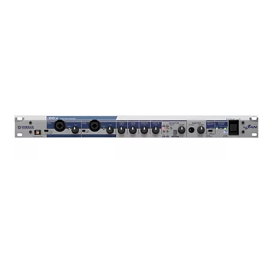
Page 7: Panel Layout
PANEL LAYOUT • Front Panel 11 12 13 14 Front Panel q [PHONTOM +48V] switch w [(HI-Z)/LINE/MIC] switch e [XLR/TRS Phone Compatible INPUT 1 and 2] jacks r [PEAK] indicators t [GAIN] controls y MONITOR [1/2 (44k)] - [7/8 (96k)] indicators... -
Page 8: Circuit Board Layout
CIRCUIT BOARD LAYOUT • Top View MLN2 DMSUB • Front View... -
Page 9: Disassembly Procedure
DISASSEMBLY PROCEDURE If you remove filament tapes for disassembling, make sure to apply them again on the occasion of reassem- bling. Top Cover (Time required: about 3 min.) 1-1. Remove the eight (8) screws marked [290]. The Rack Angle L for each side can then be removed. (Fig.1) 1-2. - Page 10 [120] [300] [310] [315] [90] [160] (Fig. 2) [90]: Bind Head Tapping Screw-B 3.0X8 MFZN2BL (EP600190) [120]: Bind Head Tapping Screw-B 3.0X8 MFZN2BL (EP600190) [160]: Bind Head Screw 4.0X6 MFZN2BL (EG340340) [300]: Cord Column WT11 (VG016600) [310]: Bind Head Tapping Screw-B 3.0X8 MFZN2BL (EP600190)
- Page 11 DM Circuit Board and DMSUB Circuit Board (Time required:about 9 min.) 4-1. Remove the top cover. (See procedure 1.) 4-2. Remove the front panel assembly. (See procedure 3.) 4-3. Remove the eight (8) knobs marked [330]. (Fig.5, Fig.6) 4-4.
- Page 12 JK2 Circuit Board (Time required:about 3 min.) 5-1. Remove the top cover. (See procedure 1.) 5-2. Remove the four (4) screws marked [120]. The JK2 circuit board can then be removed. (Fig.2) 5-3. Release the hook of Circuit Board holder, and the JK2 circuit board is removed.
- Page 13 DMSUB Sub Panel [F90] [F60] (Fig. 8) [F60]: Bind Head Tapping Screw-B 3.0X6 MFZN2BL (EP600230) [F90]: Bind Head Tapping Screw-B 3.0X6 MFZN2BL (EP600230) JK3 Circuit Board (Time required:about 7 min.) 8-1. Remove the top cover. (See procedure 1.) 8-2.
-
Page 14: Table Of Contents
LSI PIN DESCRIPTION CONTENTS YTS440B-FZ (X3009B00) MLANPH2 ................15 mLAN-NC1 (X2150A00) mLAN ..................16 MD8408B (XZ762A00) PHYSICAL LAYER ..............18 CS5351-KSR (X3782A00) A/D CONVERTER ..............18 XCR3064XL-10VQ100C (X3628D00) CPLD ..............19 HD64F3024F (X4855C00) CPU ..................20 AK5383-VS (XW272A00) A/D CONVERTER ..............20 AK4393VF-E2 (XW029A00) D/A CONVERTER ............. -
Page 15: Yts440B-Fz (X3009B00)Mlan-Ph2 (Mlan
YTS440B-FZ (X3009B00)mLAN-PH2 (mLAN Packet Handler 2) MLN2: IC7 NAME FUNCTION NAME FUNCTION IRERRN Isochronous packet error flag input (Low active) BCK128O Bit clock output for digital audio output (128Fs) IRCVN Isochronous reception enable input (Low active) MCKO Master clock output for digital audio output (64Fs to 384Fs) -
Page 16: Mlan-Nc1 (X2150A00) Mlan
(X2150A00) mLAN Node Controller 1 MLN2: IC8 NAME FUNCTION NAME FUNCTION Power terminal MCKO Master clock output for digital audio output TEST5 Test terminal WCKOD Delay output of WCKO TEST4 Test terminal IEC958O IEC60958 signal output from built-in DIT... - Page 17 NAME FUNCTION NAME FUNCTION 135 IRQ# mLAN I/O In 8415 mode, interrupt request output from 205 P00/SRXD1 I/O General purpose port 00/serial I/F PH1 block to microprocessor 206 P01/STXD1 I/O General purpose port 01/serial I/F CE8# TRI MPU CE8 signal...
-
Page 18: Md8408B (Xz762A00) Physical Layer
MD8408B (XZ762A00) PHY (Physical Layer) MLN2: IC10 NAME FUNCTION NAME FUNCTION LREQ Link request AVDD1 Analog power supply 1 DVDD Digital power supply TpBias1 A cable bias output terminal SCLK 49.152MHz link system clock TpBias0 DVSS Digital ground TpB1n... -
Page 19: Xcr3064Xl-10Vq100C (X3628D00) Cpld
XCR3064XL-10 VQ100C(X3628D00) CPLD (Complex Programmable Logic Device) MLN2: IC14 NAME FUNCTION NAME FUNCTION (Unconnected) I/O309 Output terminal which is write enable (L active) for the flash (Unconnected) memory assigned to CE9 zone of mLAN-NC1 Power supply (3.3V) (Unconnected) I/O209/TDI... -
Page 20: Hd64F3024F (X4855C00) Cpu
HD64F3024F (X4855C00) CPU DM:IC505 NAME FUNCTION NAME FUNCTION MLN2 Master /Slave control mode of ADC reserved If fs= 88.2KHz or 96KHz, then this signal is ’H’. panel Switch If Master= MLN , then this signal is ’H’. panel Switch If OPT-input is ADAT , then this signal is ’H’. -
Page 21: Ak4393Vf-E2 (Xw029A00) D/A Converter
AK4393-VF-E2 (XW029A00) D/A CONVERTER DM: IC36 NAME FUNCTION NAME FUNCTION DVSS Digital Ground Pin BVSS Substrate Ground Pin, 0V DVDD Digital Power Supply Pin, 3.3V or 5.0V VREFL Low Level Voltage Reference Input Pin MCLK Master Clock Input Pin... -
Page 22: Mbcg61594-130 (X3299A00) Atsc2A
MBCG61594-130 (X3299A00) ATSC2A DM: IC613 NAME FUNCTION NAME FUNCTION Power supply +3.3V Power supply +3.3V XTST LSI test pin PB_H_M4_SEL Port B audio data input buffer active select Ground PB_O_MUTE Port B mute WT_X CPU interface write input Ground... -
Page 23: Cs8420 (Xw559A00) Src
CS8420 (XW559A00) SRC (Sample Rate Converter) DM: IC616 NAME FUNCTION NAME FUNCTION SDA/CDOUT Serial control data I/O (I C) / data out (SPI) TCBL Transmit channel status block start AD0//CS Address bit 0 (I C) / Control port chip select (SPI) -
Page 24: Ic Block Diagram
IC BLOCK DIAGRAM TC74VHCT04AF (XT777A00) TC7WU04F (XN567A00) TC7S04F (XM182A00) TC74VHC04FT (X0195A00) TC7WU04FU (XQ805A00) Inverter Gate Hex Inverter Triple Inverter DM:IC620,IC15 DM:IC600,IC622 MLN2:IC41 TC7SH08FU (XR680A00) TC74VHC14FT (XV890A00) TC7W14F (XR336A00) 2 Input AND Gate Hex Inverter SN74HC2G14HDCTR (X3268A00) Triple Inverter DM:IC619... - Page 25 TC74VHC74FT (XV892A00) TC7WH74FU (XS680A00) SN74HC151NSR (XV734A00) Dual D-Type Flip-Flop D-Type Flip-Flop 8 to 1 Data Selector DM:IC609 DM:IC501 DM:IC511 1CLR 2CLR Data Inputs Data Inputs Outputs Data Strobe Select INPUTS OUTPUTS TC74VHC157FT (X0199A00) HD74LVC244ATELL (X2308A00) SN74LV245APWR (X3693A00) Quad 2 to 1 Multiplexer...
- Page 26 TLC2932IPWR (XV064A00) MLN2:IC2 LOGIC V PFD INHIBIT VCO INHBIT VCO V VCO OUT SELECT LOGIC V VCO V DETECTOR CHARGE PUMP SELECT BIAS VCO OUT COIN VCO GND VCO INHBIT PFD OUT PFD INHIBIT LOGIC GND LOGIC GND PFD OUT...
-
Page 27: Circuit Boards
CIRCUIT BOARDS CONTENTS DM CIRCUIT BOARD (C Version) (X4913C0) ............Page 28 DM CIRCUIT BOARD (D Version)(X4913D0) ............Page 32 MLN2 CIRCUIT BOARD (X3290C0) ..............Page 36 MLN2 CIRCUIT BOARD (X3290D0) ..............Page 37 MLN2 CIRCUIT BOARD (X3290E0) ..............Page 38 JK1 CIRCUIT BOARD (X4914C0) ................. -
Page 28: Dm Circuit Board (C Version) (X4913C0)
• DM Circuit Board (C Version) to JK1-CN101 to JK1-CN102 to JK1-CN105 to JK1-CN104 to JK2-CN202 MIC/LINE/Hi-Z MIC/LINE A’... - Page 29 JK3-CN302 not used It does the homing of the following figure and to DMSUB-CN803 it gets LED(LD1) lead. to DMSUB-CN802 Transformer(L900) Silk 1Pin 1Pin to DMSUB-CN800 to JK3-CN301 to JK2-CN201 to JK2-CN200 to JK1-CN103 to JK3-CN300 A’ Component Side...
- Page 30 • DM Circuit Board (C Version)
- Page 31 The pattern is cut. A’ Pattern Side 2NA-WC21750...
-
Page 32: Dm Circuit Board (D Version)(X4913D0)
• DM Circuit Board (D Version) to JK1-CN101 to JK1-CN102 to JK1-CN105 to JK1-CN104 to JK2-CN202 A’... - Page 33 JK3-CN302 not used It does the homing of the following figure and it gets LED(LD1) lead. to DMSUB-CN803 Transformer(L900) to DMSUB-CN802 Silk 1Pin 1Pin to DMSUB-CN800 to JK3-CN301 to JK2-CN201 to JK2-CN200 to JK1-CN103 to JK3-CN300 A’ Component Side...
- Page 34 • DM Circuit Board (D Version) A’...
- Page 35 A’ Pattern Side 2NA-WC21750...
-
Page 36: Mln2 Circuit Board (X3290C0)
The setting of DIP switch (SW1) The setting of DIP switch (SW1) to DMSUB-CN801 not used not used Jumper wire Component Side R18 is diagonally mounted. Pattern Side 2NA-WC61550 To identify it for I88X, only R115 is mounted. (i88X用であることを識別する為、R115のみ実装されています)... -
Page 37: Mln2 Circuit Board (X3290D0)
• MLN2 Circuit Board (X3290D0) not used to DMSUB-CN801 not used not used The setting of DIP switch (SW1) The setting of DIP switch (SW1) Component Side Pattern Side 2NA-WC61550 To identify it for I88X, only R115 is mounted. (i88X用であることを識別する為、R115のみ実装されています)... -
Page 38: Mln2 Circuit Board (X3290E0)
• MLN2 Circuit Board (X3290E0) not used to DMSUB-CN801 not used not used The setting of DIP switch (SW1) The setting of DIP switch (SW1) Component Side Pattern Side 2NA-WC61550 To identify it for I88X, only R115 is mounted. (i88X用であることを識別する為、R115のみ実装されています)... -
Page 39: Jk1 Circuit Board (X4914C0)
• JK1 Circuit Board to POWER SW to DM-CN900 to DM-CN600 DC IN MIDI DIGITAL STEREO OPTICAL DIGITAL STEREO A’ COAXIAL to DM-CN8 to DM-CN7 to DM-CN5 MASTER OUTPUT / +4dB(BAL)/ Component Side A’ ¥ JK1 EARTH SHEET Solder on the rounds indicated by arrows to install the JK1 EARTH SHEET. -
Page 40: Jk2 Circuit Board (X4914C0)
• JK2 Circuit Board to DM-CN2 to DM-CN1 to DM-CN3 INSERT I/O INPUT Component Side • JK3 Circuit Board to DM-CN6 to DM-CN4 to DM-CN502 • JK3 EARTH SHEET Solder on the rounds indicated by arrows to install the JK3 EARTH SHEET. -
Page 41: Dmsub Circuit Board (C Version) (X4913C0)
• DMSUB Circuit Board (C Version) to DM-CN504 to DM-CN503 to DM-CN500 Component Side to MLN2-CN6 Pattern Side • DMSUB Circuit Board (D Version) to DM-CN504 to DM-CN503 to DM-CN500 to MLN2-CN6 Component Side Pattern Side 2NA-WC21750... - Page 42 1) IEEE1394 cable C.Inspection preparation 2) PC (DOS/V type that installs WindowsXP Profes- 1) The DOS/V personal computer is connected with sional) i88X with the IEEE1394 cable, and the power of • CPU Clock: 2.2GHz or more i88X is turned on. •...
- Page 43 (NC1 Firmware is not written usually. ) the place preserved clicking "Restore" button based on data. 2. LED lighting "START" button is clicked on the following LED lighting screen clicking "LED lighting" button. I88X at that time It is confirmed that ACTIVE LED blinks.
- Page 44 The loop back "C" or "D" button is pushed (C and D The following item can be set from a set screen by are buttons for i88X). It enters the state of the loop clicking "General audio setting" button. back if "START" button is clicked on the following THRU and the word clock mastering switch etc.
- Page 45 Installed jump cable Removed chip resistor *1:R176 Left side - R164 Lower side R161, R162, R163, R164 *2:R175 Left side - R163 Lower side R172, R173, R174, R175, R176 *3:R174 Left side - R162 Lower side *4:R161 Lower side - R173 Lower side...
- Page 46 ∗ i88X DIGITAL STEREO DIGITAL STEREO MIDI OPTICAL COAXIAL INPUT INSERT I/O (BAL) DC IN OUTPUT / MASTER +4dB(BAL) ∗...
- Page 47 C:48kHz D:96kHz ∗...
- Page 48 ∗ : CH1/2 : CH3/4 : CH5/6 : CH7/8 10-10 : DIGITAL AUDIO 11-11 12-12 ADAT 13-13 15-15 24-24 : MIDI (Fig.1) ∗...
- Page 49 *1:R176 - R164 R161, R162, R163, R164 *2:R175 - R163 R172, R173, R174, R175, R176 *3:R174 - R162 *4:R161 - R173 *5:R161 - R172 (Fig.2)
- Page 50 INSPECTIONS Test Item List Test Number Item, Measuring Requirements etc. FS,Jitter, mLAN ACTIVE LED Check MIDI IN/OUT Check OPTICAL IN/OUT Check HiZ Check MIC Check ANALOG INPUT/OUTPUT, UNLOCK Check COAXIAL INPUT/OUTPUT Check ADAT 96KHz INTPUT/OUTPUT Check ADAT 48KHz INTPUT/OUTPUT Check...
- Page 51 T01: FS, Jitter, mLAN ACTIVE LED, mLAN Terminal Check T02: MIDI IN/OUT Check [Description] [Description] • Checks that the FS on the main unit switches over Checks that the test MIDI data sent to the MIDI IN correctly by changing the FS on the mLAN side.
- Page 52 [Check Item] [Check Item] 3-1 Confirm that the music data is played back correctly 5-1 Make sure that the signal(+4+/-2dBu, 10K ohm from the Optical Input Device. load) is output from the OUTPUT 1 jack correctly. Make sure that the music data is played back Also, confirm that the distortion rate is 0.06% or...
- Page 53 6-11Turn the [GAIN CH1] knob full clockwise for the the same level as above. maximum volume level and apply a signal(-34dBu) Make sure that the signal level of OUTPUT 1 is - to the INPUT 1 jack. 80dBu or less.
- Page 54 +/-1dB against the standard level at 1KHz. 6-13Make sure that the signal(+4+/-3dBu, 10K ohm Also change the frequency to 20KHz, make sure of load) is output from the OUTPUT 3 jack.
- Page 55 OUTPUT 2 jack. [Procedure] Make sure that the MONITOR SELECT 7/8 LED 8-1 Interconnect the COAXIAL IN/OUT terminals on lights up. the O1V96 and the COAXIAL OUT/IN terminals on the main unit. T07: COAXIAL IN/OUT Check Interconnect the ADAT IN/OUT terminals on the...
- Page 56 LoopBack Off, FS=48KHz, 11-3Measure the consumption current over 1 minute Connection Setting(Set to after turning on the power of the main unit. "Master=i88x" first, and then [Check Item] disconnect the mLAN cable.) 11-1Confirm that the click noise level at each jack meets Main Unit Setting: the following conditions.
- Page 57 i88X...
- Page 58 i88X...
- Page 59 i88X...
- Page 60 i88X...
- Page 61 i88X...
- Page 62 i88X...
- Page 63 i88X...
- Page 64 It always works the normal mode. The confirmation of the firmware version 1. While pressing the "MONITOR SELECT" button on the i88X’s front panel, turn the power on. 2. By the combination of the blink number(s) of the three LEDs (1/2[44K], 3/4[48K] and DIGITAL) on the upper section of MONITOR display, the version number is expressed.
- Page 65 [IC505 CPU] DIGITAL...
- Page 66 i88X...
-
Page 67: Parts List
AUDIO / MIDI INTERFACE PARTS LIST CONTENTS OVERALL ASSEMBLY ELECTRICAL PARTS Note) DESTINATION ABBREVIATIONS Australian model Chinese model British model South-east Asia model Canadian model Taiwan model German model U.S.A. model European model General export model (110V) French model General export model (220V) North European model N,X: General export model Indonesian model... - Page 68 OVERALL ASSEMBLY ACCESSORIES F100a F100 F130 F110 F120...
- Page 69 AC Adapter PA-51 O(Chinese model) WB122200 Interface Cable IEEE1394 6P-6P2.0m X4149B00 CD-ROM Tool for i88X/mLAN CD-ROM CD-ROM Plug-in Effect CD-ROM (X4295A0) Accessory of the CD-ROM is not a Service Parts. Please contact sales side. * : New parts RANK : Japan only...
-
Page 70: Electrical Parts
ELECTRICAL PARTS DESCRIPTION REMARKS PART NO. QTY RANK REF NO. ELECTRICAL PARTS WC161900 Circuit Board DM(DM+DMSUB) i88X WC217600 Circuit Board (WC16190)(X4913C0) WC217700 Circuit Board (WC15660)(X4914C0) WC217800 Circuit Board (WC15660)(X4914C0) WC615500 Circuit Board mLAN2 (WC15660)(X4914C0) (X3290C0/D0/EO) WC161900 Circuit Board DM(DM+DMSUB) Cable 17P 100L P=1.5... - Page 71 PART NO. DESCRIPTION REMARKS QTY RANK REF NO UU147470 Electric Capacitor C0097 47.00 25.0V UU147470 -0102 Electric Capacitor 47.00 25.0V US145100 C0103 Ceramic Capacitor-F (chip) 0.1000 25V Z US145100 -0105 Ceramic Capacitor-F (chip) 0.1000 25V Z US062220 C0106 Ceramic Capacitor-SL(chip)
- Page 72 PART NO. DESCRIPTION REMARKS QTY RANK REF NO. US064100 Ceramic Capacitor-B (chip) C0178 0.0100 50V K US064100 C0179 Ceramic Capacitor-B (chip) 0.0100 50V K US145100 C0180 Ceramic Capacitor-F (chip) 0.1000 25V Z WD093700 C0181 Electrolytic Cap. (chip) 68U 20V 20SPS68M...
- Page 73 DESCRIPTION REMARKS PART NO. QTY RANK REF NO US061330 Ceramic Capacitor-CH(chip) C0275 33P 50V J US061330 -0286 Ceramic Capacitor-CH(chip) 33P 50V J UU148220 Electric Capacitor C0287 220.00 25.0V UU148220 C0288 Electric Capacitor 220.00 25.0V US061330 Ceramic Capacitor-CH(chip) C0289 33P 50V J...
- Page 74 PART NO. DESCRIPTION REMARKS QTY RANK REF NO. US135330 Ceramic Capacitor-F (chip) C0630 0.3300 16V Z US145100 C0631 Ceramic Capacitor-F (chip) 0.1000 25V Z US145100 -0633 Ceramic Capacitor-F (chip) 0.1000 25V Z US135330 C0634 Ceramic Capacitor-F (chip) 0.3300 16V Z...
- Page 75 PART NO. DESCRIPTION REMARKS QTY RANK REF NO US126100 Ceramic Capacitor-F (chip) C0985 1.0000 10V Z US064100 C0986 Ceramic Capacitor-B (chip) 0.0100 50V K VK025700 CN001 Wire Trap 52147 13P TE VK025300 CN002 Wire Trap 52147 9P TE VB390400...
- Page 76 PART NO. DESCRIPTION REMARKS QTY RANK REF NO. XF291A00 IC025 UPC4570G2 OP AMP XQ824A00 IC026 NJM4556AD OP AMP X5025A00 IC027 NJM4580M-D(TE2) OP AMP X5025A00 -035 NJM4580M-D(TE2) OP AMP XW029A00 IC036 AK4393VF-E2 OP AMP XJ598A00 IC037 NJM78L05UA D/A CONVERTER XF291A00...
- Page 77 DESCRIPTION REMARKS PART NO. QTY RANK REF NO WC617300 LD503 SEL2210W RE 5/6 88K VS079300 LD504 SPR-39MVWF 7/8 96K RD155330 Carbon Resistor (chip) R0001 330.0 1/4 J DIGITAL RD259100 R0002 Carbon Resistor (chip) 1.0M 0.1 J RD358100 Carbon Resistor (chip) R0003 100.0K 63M J...
- Page 78 PART NO. DESCRIPTION REMARKS QTY RANK REF NO. V I 1 9 8 4 0 0 Carbon Resistor (chip) R0106 27.0K 1/10 D V I 1 9 8 4 0 0 -0109 Carbon Resistor (chip) 27.0K 1/10 D RD258100...
- Page 79 PART NO. DESCRIPTION REMARKS QTY RANK REF NO V I 1 9 2 9 0 0 Carbon Resistor (chip) -0205 150.0 1/10 D RD254390 R0206 Carbon Resistor (chip) 39.0 0.1 J RD254390 R0207 Carbon Resistor (chip) 39.0 0.1 J...
- Page 80 PART NO. DESCRIPTION REMARKS QTY RANK REF NO. RD258100 Carbon Resistor (chip) -0383 100.0K 0.1 J RD257100 R0384 Carbon Resistor (chip) 10.0K 0.1 J RD257100 -0399 Carbon Resistor (chip) 10.0K 0.1 J RD150000 R0400 Carbon Resistor (chip) 0.0 1/4 J...
- Page 81 PART NO. DESCRIPTION REMARKS QTY RANK REF NO RD355220 Carbon Resistor (chip) R0606 220.0 63M J RD154470 R0607 Carbon Resistor (chip) 47.0 1/4 J RD154470 R0608 Carbon Resistor (chip) 47.0 1/4 J RD356220 R0609 Carbon Resistor (chip) 2.2K 63M J...
- Page 82 PART NO. DESCRIPTION REMARKS QTY RANK REF NO. RD258100 Carbon Resistor (chip) R0930 100.0K 0.1 J RD259100 R0931 Carbon Resistor (chip) 1.0M 0.1 J RD254100 R0932 Carbon Resistor (chip) 10.0 0.1 J WA295000 R0933 Carbon Resistor (chip) 0.15 1/2 F...
- Page 83 DESCRIPTION REMARKS PART NO. QTY RANK REF NO WC215300 Cable 13P 275L P=2.0 WC215400 Cable 14P 250L P=2.0 WC215500 Cable 15P 130L P=2.0 WC130800 Holder, Jack WC130900 Holder, Jack-4 V 4 4 5 0 1 0 0 LED Spacer JK1 Earth Sheet 43.2X278.2 t=0.1...
- Page 84 PART NO. DESCRIPTION REMARKS QTY RANK REF NO. VG893800 Bind Head Tapping Screw-P 2.0X6 MFZN2BL US064100 Ceramic Capacitor-B (chip) C0002 0.0100 50V K VE326600 Monolithic Mylar Capacitor C0003 0.33 50V J US064100 Ceramic Capacitor-B (chip) C0005 0.0100 50V K...
- Page 85 PART NO. DESCRIPTION REMARKS QTY RANK REF NO X4182A00 IC019 M51957AFP XR336A00 IC021 TC7W14F INVERTER XW148A00 IC022 HD74LVC245ATELL TRANSCEIVER XZ287A00 IC022 SN74LVC245APWR TRANSCEIVER XW148A00 IC026 HD74LVC245ATELL TRANSCEIVER XZ287A00 IC026 SN74LVC245APWR TRANSCEIVER XW148A00 IC035 HD74LVC245ATELL TRANSCEIVER XZ287A00 IC035 SN74LVC245APWR TRANSCEIVER...
- Page 86 PART NO. DESCRIPTION REMARKS QTY RANK REF NO. WA516800 Resistor Array (Chip) RA001 CN1E4KTTD103J WA512000 -021 Resistor Array (Chip) CN1E4KTTD101J WA516800 RA022 Resistor Array (Chip) CN1E4KTTD103J WA516800 -027 Resistor Array (Chip) CN1E4KTTD103J WA516000 RA028 Resistor Array (Chip) CN1E4KTTD472J WA516800...
- Page 87 <P.1> i88X BLOCK DIAGRAM i88X MLN2 DMSUB Phantom IC8-256PIN IC9-8PIN (GUID/Modul Name/Config) +48V -9VA -9VA +3.3VD 1,19,29,34,59,134 14,15 +3.3VD EEPROM 147,160,175194,219 Phantom SW MIDI(UART) Audio Data (To MLN2) CH1 Peak LED CH2 Peak LED (16KBit) MIDI IN/OUT IC10-64PIN 228,242 PHY-LINK I/F...
- Page 88 <P.2> i88X OVERALL CIRCUIT DIAGRAM 1/12 (DM 1/5) i88X REGULATOR +9V REGULATOR -9V Not installed REGULATOR (VARIABLE) REGULATOR +5V ANALOG Circuit block Component Side REGULATOR (VARIABLE) Digital Circuit block Power Supply Circuit block FG2,FG3 and FG4 are solid pattern. (Component side, Pattern side)
- Page 89 <P.3> i88X OVERALL CIRCUIT DIAGRAM 3/12 (DM 3/5) i88X Not installed (1FS is counted by the timer.) Not installed RESET Not installed MONITOR D-FF In the usual case: Pull-Up via 10k ohms SELECT In case of CN501 connection: Low Fs(HOLD)
- Page 90 <P.4> i88X OVERALL CIRCUIT DIAGRAM 5/12 (DM 5/5) i88X OVERALL CIRCUIT DIAGRAM 6/12 (DMSUB) i88X Not installed Not connected i88X OVERALL CIRCUIT DIAGRAM 7/12 (MLN2 1/3) NOTE) NOTATION OF RESISTOR * All the resistors, unless otherwise specified, are 1/16W chip resistors.
- Page 91 <P.5> i88X OVERALL CIRCUIT DIAGRAM 8/12 (MLN2 2/3) i88X MLN2 Not installed Not installed CPLD Not installed Not installed Not installed Not installed Not installed Not installed RESET INVERTER Not installed Not installed ( ) : Ceramic Capacitor 28CC1-8827928 4 2/3...
- Page 92 <P.6> <P.6> i88X OVERALL CIRCUIT DIAGRAM 10/12 (JK1) i88X OVERALL CIRCUIT DIAGRAM 11/12 (JK2) i88X to DM-CN1 to DM-CN2 to DM-CN3 i88X OVERALL CIRCUIT DIAGRAM 12/12 (JK3) PHONES MASTER VOLUME ADAT DOUBLE OPTICAL ADAT NORMAL SELECT DIGITAL ADAT MASTER CLOCK...