Clevo P170EM Service Manual
Hide thumbs
Also See for P170EM:
- Service manual (122 pages) ,
- Concise user manual (196 pages) ,
- Concise user manual (186 pages)
Table of Contents
Advertisement
Advertisement
Table of Contents

Related Manuals for Clevo P170EM


Summary of Contents for Clevo P170EM
- Page 1 P170EM SERVICE MANUAL Downloaded from www.Manualslib.com manuals search engine...
- Page 2 Downloaded from www.Manualslib.com manuals search engine...
-
Page 3: Notebook Computer
Preface Notebook Computer P170EM Service Manual Downloaded from www.Manualslib.com manuals search engine... - Page 4 Preface Notice The company reserves the right to revise this publication or to change its contents without notice. Information contained herein is for reference only and does not constitute a commitment on the part of the manufacturer or any subsequent ven- dor.
- Page 5 This manual is intended for service personnel who have completed sufficient training to undertake the maintenance and inspection of personal computers. It is organized to allow you to look up basic information for servicing and/or upgrading components of the P170EM se- ries notebook PC.
- Page 6 Preface IMPORTANT SAFETY INSTRUCTIONS Follow basic safety precautions, including those listed below, to reduce the risk of fire, electric shock and injury to per- sons when using any electrical equipment: 1. Do not use this product near water, for example near a bath tub, wash bowl, kitchen sink or laundry tub, in a wet basement or near a swimming pool.
-
Page 7: Instructions For Care And Operation
Preface Instructions for Care and Operation The notebook computer is quite rugged, but it can be damaged. To prevent this, follow these suggestions: Don’t drop it, or expose it to shock. If the computer falls, the case and the components could be damaged. Do not expose the computer Do not place it on an unstable Do not place anything heavy... - Page 8 Preface Avoid interference. Keep the computer away from high capacity transformers, electric motors, and other strong mag- netic fields. These can hinder proper performance and damage your data. Take care when using peripheral devices. Removal Warning Use only approved brands of Unplug the power cord before When removing any peripherals.
-
Page 9: Battery Precautions
Preface Battery Precautions • Only use batteries designed for this computer. The wrong battery type may explode, leak or damage the computer. • Do not continue to use a battery that has been dropped, or that appears damaged (e.g. bent or twisted) in any way. Even if the computer continues to work with a damaged battery in place, it may cause circuit damage, which may possibly result in fire. -
Page 10: Related Documents
Preface Related Documents You may also need to consult the following manual for additional information: User’s Manual on Disc This describes the notebook PC’s features and the procedures for operating the computer and its ROM-based setup pro- gram. It also describes the installation and operation of the utility programs provided with the notebook PC. System Startup 1. -
Page 11: Table Of Contents
Preface Contents Introduction ..........1-1 Top without Fingerprint ..............A-4 Bottom ..................A-5 Overview ..................1-1 LCD ....................A-6 External Locator - Top View with LCD Panel Open ......1-4 HDD ....................A-7 External Locator - Front & Right side Views .........1-5 COMBO ..................A-8 External Locator - Left Side &... - Page 12 Preface PCH 5/9 - PCI, USB, RSVD ............B-25 P170 LED Board ................B-57 PCH 6/9 - GPIO, CPU ..............B-26 P170 Click Board ................B-58 PCH 7/9 - Power ................B-27 P170 Fingerprint Board ..............B-59 PCH 8/9 - Power ................B-28 P150 HDD Board ................B-60 PCH 9/9 - GND ................
-
Page 13: Introduction
Chapter 1: Introduction Overview This manual covers the information you need to service or upgrade the P170EM series notebook computer. Information about operating the computer (e.g. getting started, and the Setup utility) is in the User’s Manual. Information about driv- ers (e.g. -
Page 14: Specifications
Introduction Specifications Processor Options Intel® Core™ i7 Processor 17.3" (46.94cm) FHD (1920 * 1080) i7-3920XM (2.90GHz) BIOS 8MB L3 Cache, 22nm, DDR3-1600MHz, TDP 55W AMI BIOS (48Mb SPI Flash-ROM) Intel® Core™ i7 Processor Storage i7-3820QM (2.70GHz) One Changeable 2.5" (6cm) 9.5mm (h) SATA (Serial) Hard Disk Drives 8MB L3 Cache, 22nm, DDR3-1600MHz, TDP 45W Latest Specification Information... -
Page 15: Overview
Introduction Security Interface Security (Kensington® Type) Lock Slot Three USB 3.0 Ports (Including one AC/DC Powered USB/ eSATA port) BIOS Password (Factory Option) Fingerprint Reader Module One USB 2.0 Port Audio One eSATA Port (USB 3.0 Port Combined) High Definition Audio Compliant Interface One HDMI-Out (1.4a) Port THX TruStudio Pro One DVI-Out Port... -
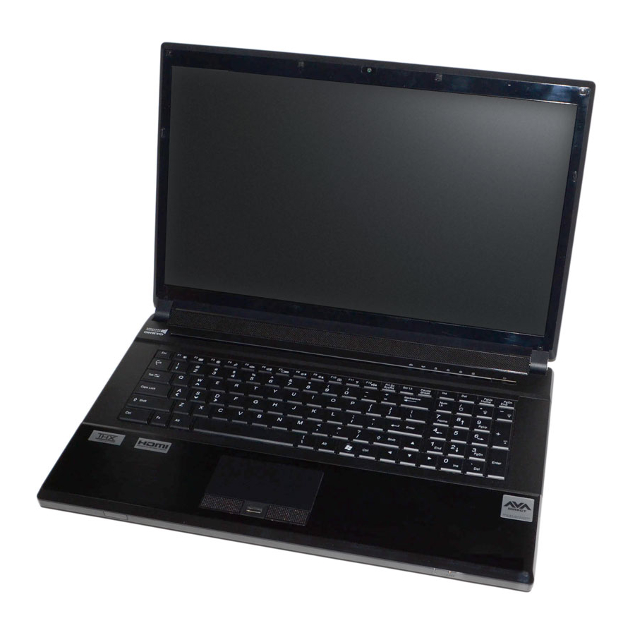
Page 16: External Locator - Top View With Lcd Panel Open
Introduction External Locator - Top View with LCD Panel Open Figure 1 Top View 1. PC Camera 2. LCD 3. LED Status Indicators 4. Power Button 5. Speakers 6. Keyboard 7. Built-In Microphone 8. TouchPad and Buttons 9. Fingerprint Reader (Optional) 1 - 4 External Locator - Top View with LCD Panel Open Downloaded from www.Manualslib.com... -
Page 17: External Locator - Front & Right Side Views
Introduction External Locator - Front & Right side Views Figure 2 Front Views 1. LED Power Indicators Figure 3 Right Side Views 1. Optical Device Drive Bay 2. Emergency Eject Hole 3. Headphone Jack 4. Microphone Jack 5. S/PDIF-Out Jack 6. -
Page 18: External Locator - Left Side & Rear View
Introduction External Locator - Left Side & Rear View Figure 4 Left Side View 1. Mini-IEEE 1394a Port 2. RJ-45 LAN Jack 3. USB 3.0 Port / USB Charge 4. USB 3.0 Port 5. Combined eSATA/ Powered USB 3.0 Port 6. -
Page 19: External Locator - Bottom View
Introduction External Locator - Bottom View Figure 6 Bottom View 1. Sub Woofer 2. Fan Outlet/Intake 3. Component Bay Cover 4. Primary HDD Bay 5. Secondary HDD 6. Battery Overheating To prevent your com- puter from overheating make sure nothing blocks the vent/fan in- takes while the com-... -
Page 20: Mainboard Overview - Top (Key Parts)
Introduction Mainboard Overview - Top (Key Parts) Figure 7 Mainboard Top Key Parts 1. Platform Controller Hub 2. Audio Codec 3. KBC ITE IT8519E 1 - 8 Mainboard Overview - Top (Key Parts) Downloaded from www.Manualslib.com manuals search engine... -
Page 21: Mainboard Overview - Bottom (Key Parts)
Introduction Mainboard Overview - Bottom (Key Parts) Figure 8 Mainboard Bottom Key Parts 1. VGA-Card Connector 2. CPU Socket (no CPU installed) 3. Memory Slots DDR3 SO-DIMM 4. Hard Disk Connector 5. Mini-Card MSATA Connector 6. RTL8411 Mainboard Overview - Bottom (Key Parts) 1 - 9 Downloaded from www.Manualslib.com manuals search engine... -
Page 22: Mainboard Overview - Top (Connectors)
Introduction Mainboard Overview - Top (Connectors) Figure 9 Mainboard Top Connectors 1. CCD Connector 2. USB 3.0 Port / eSATA 3. Multi-in-1 Card Reader 4. TouchPad Cable Connector 5. Microphone Cable Connector 6. Keyboard Cable Connector 7. CMOS Battery Connector 8. -
Page 23: Mainboard Overview - Bottom (Connectors)
Introduction Mainboard Overview - Bottom (Connectors) Figure 10 Mainboard Bottom Connectors 1. DC-In Jack 2. DVI-Out Port 3. HDMI-Out Port 4. Display Port 5. VGA Fan Cable Connector 6. Sub Woofer Cable Connector 7. CPU Fan Cable Connector 8. USB 3.0 Ports 9. - Page 24 Introduction 1 - 12 Downloaded from www.Manualslib.com manuals search engine...
-
Page 25: Disassembly
Chapter 2: Disassembly Overview This chapter provides step-by-step instructions for disassembling the P170EM series notebook’s parts and subsystems. When it comes to reassembly, reverse the procedures (unless otherwise indicated). We suggest you completely review any procedure before you take the computer apart. -
Page 26: Maintenance Tools
Disassembly NOTE: All disassembly procedures assume that the system is turned OFF, and disconnected from any power supply (the battery is removed too). Maintenance Tools The following tools are recommended when working on the notebook PC: • M3 Philips-head screwdriver •... -
Page 27: Maintenance Precautions
Disassembly Maintenance Precautions The following precautions are a reminder. To avoid personal injury or damage to the computer while performing a re- moval and/or replacement job, take the following precautions: Power Safety Warning 1. Don't drop it. Perform your repairs and/or upgrades on a stable surface. If the computer falls, the case and other Before you undertake components could be damaged. -
Page 28: Disassembly Steps
Disassembly Disassembly Steps The following table lists the disassembly steps, and on which page to find the related information. PLEASE PERFORM THE DISASSEMBLY STEPS IN THE ORDER INDICATED. To remove the Battery: To remove and install a Processor: 1. Remove the battery page 2 - 5 1. -
Page 29: Removing The Battery
Disassembly Removing the Battery 1. Turn the computer off, and turn it over. 2. Slide the latch in the direction of the arrow (Figure 1a Figure 1 3. Slide the latch in the direction of the arrow, and hold it in place (Figure 1a Battery Removal 4. -
Page 30: Removing The Hard Disk Drive
Disassembly Removing the Hard Disk Drive Figure 2 HDD Assembly The hard disk drive can be taken out to accommodate other 2.5" serial (SATA) hard disk drives with a height of 9.5mm Removal (h). Follow your operating system’s installation instructions, and install all necessary drivers and utilities (as outlined in Chapter 4 of the User’s Manual) when setting up a new hard disk. - Page 31 Disassembly 4. Slide the HDD assembly in the direction of the arrow (Figure 3c Figure 3 5. Remove the hard disk assembly (Figure 3d HDD Assembly 6. Remove screws & and the insulation plate (Figure 3e Removal (cont’d.) 7. Reverse the process to install a new hard disk (do not forget to replace all the screws and covers). c.
- Page 32 Disassembly Inserting the Hard Disk Into the HDD Bay Figure 4 1. Make sure the HDD assembly is aligned with the black taped area (Figure 4a Inserting the Hard 2. When aligned, carefully insert the HDD assembly into the case so that the connectors line up (Figure 4a Disk Into the HDD 3.
-
Page 33: Removing The Optical (Cd/Dvd) Device
Disassembly Removing the Optical (CD/DVD) Device Figure 5 Optical Device 1. Turn off the computer, and remove the battery (page 2 - Removal 2. Locate the secondary hard disk bay cover and remove screws & (Figure 5a 3. Remove the hard disk bay cover (Figure 5b a. -
Page 34: Removing The Hard Disk From The Secondary Hdd Bay
Disassembly Removing the Hard Disk from the Secondary HDD Bay Figure 6 Note that the secondary hard disk (if installed) is located under the optical device bay (CD/DVD). Secondary HDD Assembly Removal 1. Turn off the computer, and turn it over, remove the battery (page 2 - 5) and optical device (page 2 -... - Page 35 Disassembly Remove screws and the insulation plate (Figure 7d Figure 7 Secondary HDD Assembly Removal d. Remove the screws and the insulation plate. 6. Reverse the process to install a new disk (make sure you install the insulation plate). 7. Slide the HDD assembly into the bay at an angle as illustrated. 8.
-
Page 36: Removing The Primary System Memory (Ram)
Disassembly Removing the Primary System Memory (RAM) Figure 8 RAM Module The computer has four memory sockets for 204 pin Small Outline Dual In-line (SO-DIMM) DDR III (DDR3) type memory Removal modules (see “Memory” on page 1 - 2 ). The total memory size is automatically detected by the POST routine once you turn a. - Page 37 Disassembly 4. Lift the component bay cover off the computer case. The modules will be visible at point (Figure 9c Figure 9 5. Gently pull the two release latches ( ) on the sides of the memory socket(s) in the direction indicated below &...
-
Page 38: Removing The Secondary System Memory (Ram)
Disassembly Removing the Secondary System Memory (RAM) Figure 10 RAM Module Removal Memory Upgrade Process a. Remove 1. Turn off the computer, and turn it over, remove the battery (page 2 - 5) and the component bay cover. cover module. 2. - Page 39 Disassembly 5. Disconnect the keyboard ribbon cable from the locking collar socket by using a small flat-head screwdriver Figure 11 to pry the locking collar pins away from the base. (Figure 11e). RAM Module 6. Remove the keyboard and the memory sockets &...
-
Page 40: Removing The Wireless Lan Module
Disassembly Removing the Wireless LAN Module Figure 12 Wireless LAN 1. Turn off the computer, remove the battery (page 2 - 5) and the keyboard (page 2 - Module Removal 2. The Wireless LAN module will be visible at point under the keyboard (Figure 12a). -
Page 41: Removing And Installing The Processor
Disassembly Removing and Installing the Processor Figure 13 Processor Processor Removal Procedure Removal 1. Turn off the computer, remove the battery (page 2 - 5), and component bay cover (page 2 - 10). Procedure 2. Remove screws from the heat sink unit in the order indicated on the label (i.e screw 4 first through to screw 1 last Figure 13a) - Page 42 Disassembly 4. Turn the release latch towards the unlock symbol , to release the CPU (Figure 14c). Figure 14 5. Carefully (it may be hot) lift the CPU up out of the socket (Figure 14d). Processor Removal 6. See page 2 - 19 for information on inserting a new CPU.
- Page 43 Disassembly Processor Installation Procedure Figure 15 Processor 1. Insert the CPU , pay careful attention to the pin alignment (Figure 15a), it will fit only one way (DO NOT Installation FORCE IT!), and turn the release latch towards the lock symbol (Figure 15b).
-
Page 44: Removing And Installing The Video Card
Disassembly Removing and Installing the Video Card Figure 16 Video Card Video Card Removal Procedure Removal Procedure Turn off the computer, turn it over and remove the battery (page 2 - 5) and component cover (page 2 - Remove screws from the heat sink unit in the order indicated on the label (i.e screw 7 first through to screw a. - Page 45 Disassembly Installing a New Video Card Figure 17 Installing a New Prepare to fit the video card into the slot by holding it at about a 30° angle (Figure 17e). Video Card The card needs to be fully into the slot, and the video card and socket have a guide-key and pin which align to allow the card to fit securely (Figure 17f)
-
Page 46: Removing The Microphone
Disassembly Figure 18 Removing the Microphone Microphone Removal 1. Turn off the computer, and remove the battery (page 2 - 5), component bay cover (page 2 - 10), processor (page 17), hard disk (page 2 - (page 2 - 10), optical device (page 2 - 9), and video card (page 2 -... -
Page 47: Part Lists
Part Lists Appendix A: Part Lists This appendix breaks down the P170EM series notebook’s construction into a series of illustrations. The component part numbers are indicated in the tables opposite the drawings. Note: This section indicates the manufacturer’s part numbers. Your organization may use a different system, so be sure to cross-check any relevant documentation. -
Page 48: Part List Illustration Location
Part Lists Part List Illustration Location The following table indicates where to find the appropriate part list illustration. Table A- 1 Part List Illustration Location Parts Top with Fingerprint page A - 3 Top without Fingerprint page A - 4 Bottom page A - 5 page A - 6... -
Page 49: Top With Fingerprint
Part Lists Top with Fingerprint Figure A - 1 Top with Fingerprint Top with Fingerprint A - 3 Downloaded from www.Manualslib.com manuals search engine... -
Page 50: Top Without Fingerprint
Part Lists Top without Fingerprint Figure A - 2 Top without Fingerprint A - 4 Top without Fingerprint Downloaded from www.Manualslib.com manuals search engine... -
Page 51: Bottom
Part Lists Bottom Figure A - 3 Bottom Bottom A - 5 Downloaded from www.Manualslib.com manuals search engine... -
Page 52: Lcd
Part Lists Figure A - 4 A - 6 LCD Downloaded from www.Manualslib.com manuals search engine... -
Page 53: Hdd
Part Lists Figure A - 5 (非耐落) HDD A - 7 Downloaded from www.Manualslib.com manuals search engine... -
Page 54: Combo
Part Lists COMBO Figure A - 6 COMBO A - 8 COMBO Downloaded from www.Manualslib.com manuals search engine... -
Page 55: Dvd-Dual Drive
Part Lists DVD-Dual Drive Figure A - 7 DVD-Dual Drive DVD-Dual Drive A - 9 Downloaded from www.Manualslib.com manuals search engine... - Page 56 Part Lists A - 10 Downloaded from www.Manualslib.com manuals search engine...
- Page 57 Schematic Diagrams Appendix B: Schematic Diagrams This appendix has circuit diagrams of the P170EM notebook’s PCB’s. The following table indicates where to find the appropriate schematic diagram. Diagram - Page Diagram - Page Diagram - Page Table B - 1...
-
Page 58: Schematic Diagrams
Schematic Diagrams System Block Diagram P150EM Chief River System Block Diagram AUDIO BOARD VDD3,VDD5 PHONE JACK x4, USB x1 SHEET 40 P150 ODD BOARD 5V,3.3V,5VS,3VS,1.5VS P150 CLICK & F/P BOARD <=5" PCIE*16 1.05VS 1067/1333/1600 MHz DDR3 / 1.5V Ivy Bridge POWER LED BOARD 1.5V,VTT_MEM <=4.3"... -
Page 59: Tpm
Schematic Diagrams 3.3VS TPM 1.2 TPM Function ¤£¤W¥ó C786 C787 C788 C789 20,35 LPC_AD0 LAD0 VDD1 *0.1u_16V_Y 5V_04 *0.1u_16V_Y 5V_04 *0.1u_16V_Y 5V_04 *1u_10V_06 20,35 LPC_AD1 LAD1 VDD2 20,35 LPC_AD2 LAD2 VDD3 20,35 LPC_AD3 LAD3 VDD3 PCLK_TPM LCLK 20,35 LPC_FRAME# LFRAME# 4,14,24 PLT_RST# LRESET#... -
Page 60: Processor 1/7
Schematic Diagrams Processor 1/7 Ivy Bridge Processor 1/7 ( DMI,PEG,FDI ) 1.05VS_VTT U32A 20 mil PEG_IRCOMP_R 24.9_1%_04 PEG_ICOMPI PEG_ICOMPO DMI_TXN0 DMI_RX#[0] PEG_RCOMPO PEG_RXN[0..15] 14 DMI_TXN1 DMI_RX#[1] DMI_TXN2 DMI_RX#[2] C433 0.22u_10V_X5R_04 PEG_RXN0 DMI_TXN3 DMI_RX#[3] PEG_RX#[0] C467 0.22u_10V_X5R_04 PEG_RXN1 PEG_RX#[1] C431 0.22u_10V_X5R_04 PEG_RXN2 DMI_TXP0 DMI_RX[0]... -
Page 61: Processor 2/7
Schematic Diagrams Processor 2/7 Ivy Bridge Processor 2/7 ( CLK,MISC,JTAG ) PU/PD for JTAG signals 1.05VS_VTT XDP_TMS 51_04 XDP_TDI_R 51_04 XDP_PREQ# *51_04 XDP_TDO_R U32B R308 51_04 XDP_TCLK R309 51_04 XDP_TRST# 51_04 CLK_EXP_P 21 BCLK PROC_SELET H_SNB_IVB# CLK_EXP_N 21 PROC_SELECT# BCLK# 3.3VS SKTOCC# AN34... -
Page 62: Processor 3/7
Schematic Diagrams Processor 3/7 Ivy Bridge Processor 3/7 ( DDR3 ) U32C U32D 10,11 M_A_DQ[63:0] M_A_CLK_DDR0 10 12,13 M_B_DQ[63:0] M_B_CLK_DDR0 13 SA_CK[0] SB_CK[0] M_A_CLK_DDR#0 10 M_B_CLK_DDR#0 13 SA_CLK#[0] SB_CLK#[0] M_A_DQ0 M_B_DQ0 M_A_CKE0 10 M_B_CKE0 13 SA_DQ[0] SA_CKE[0] SB_DQ[0] SB_CKE[0] M_A_DQ1 M_B_DQ1 SA_DQ[1] SB_DQ[1]... -
Page 63: Processor 4/7
Schematic Diagrams Processor 4/7 Ivy Bridge Processor 4/7 ( POWER ) POWER U32F PROCESSOR CORE POWER PROCESSOR UNCORE POWER VCORE 8.5A 1.05VS_VTT 1.05VS_VTT AG35 VCC1 AG34 AH13 ICCMAX Maximum Processor AG33 VCC2 VCCIO1 AH10 VCC3 VCCIO2 AG32 AG10 C273 C449 C257 C236 C487... -
Page 64: Processor 5/7
Schematic Diagrams Processor 5/7 Ivy Bridge Processor 5/7 ( GRAPHICS POWER ) 1.5VS_CPU R175 100_04 POWER AO3402L V_SM_VREF V_SM_VREF_CNT U32G VGFX_CORE AT24 AK35 C245 R178 VCC_GT_SENSE 45 AT23 VAXG1 VAXG_SENSE AK34 VAXG2 VSSAXG_SENSE VSS_GT_SENSE 45 AT21 C187 C170 C549 C186 C171 0.1u_10V_X5R_04 100_04... -
Page 65: Processor 6/7
Schematic Diagrams Processor 6/7 Ivy Bridge Processor 6/7 ( GND ) U32H U32I AT35 AJ22 VSS1 VSS81 AT32 AJ19 VSS2 VSS82 AT29 AJ16 VSS3 VSS83 VSS161 VSS234 AT27 AJ13 VSS4 VSS84 VSS162 VSS235 AT25 AJ10 VSS5 VSS85 VSS163 VSS236 AT22 AT19 VSS6 VSS86... -
Page 66: Processor 7/7
Schematic Diagrams Processor 7/7 Ivy Bridge Processor 7/7 ( RESERVED ) U32E CFG Straps for Processor AH27 VCC_DIE_SENSE CFG0 AK28 AH26 CFG[0] VSS_DIE_SENSE AK29 PEG Static Lane Reversal - CFG2 is for the 16x CFG[1] CFG2 AL26 CFG[2] AL27 CFG[3] CFG4 AK26 CFG2... -
Page 67: Ddriii Cha So-Dimm_0
Schematic Diagrams DDRIII CHA SO-DIMM_0 Channel A SO-DIMM 0 CHANGE TO STANDARD JD IMM3A 5,11 M_A_A[15:0] M_A_DQ[63:0] 5,11 M_A_A0 M_A_DQ0 JDIMM3B M_A_A1 M_A_DQ1 M_A_A2 M_A_DQ2 M_A_A3 M_A_DQ3 1.5V M_A_A4 M_A_DQ4 M_A_A5 M_A_DQ5 VD D1 VSS16 M_A_A6 M_A_DQ6 VD D2 VSS17 M_A_A7 M_A_DQ7 VD D3... -
Page 68: Ddriii Cha So-Dimm_1
Schematic Diagrams DDRIII CHA SO-DIMM_1 Channel A SO-DIMM 1 CHANGE TO STANDARD JD IMM1A 5,10 M_A_A[15:0] M_A_DQ[63:0] 5,10 M_A_A0 M_A_DQ0 JDIMM1B M_A_A1 M_A_DQ1 M_A_A2 M_A_DQ2 M_A_A3 M_A_DQ3 1.5V M_A_A4 M_A_DQ4 M_A_A5 M_A_DQ5 VD D1 VSS16 M_A_A6 M_A_DQ6 VD D2 VSS17 M_A_A7 M_A_DQ7 VD D3... -
Page 69: Ddriii Chb So-Dimm_0
Schematic Diagrams DDRIII CHB SO-DIMM_0 Channel B SO-DIMM 0 CHANGE TO STANDARD JDIMM2A 5,13 M_B_B[15:0] M_B_DQ[63:0] 5,13 M_B_B0 M_B_DQ0 JDIMM2B M_B_B1 M_B_DQ1 M_B_B2 M_B_DQ2 M_B_B3 M_B_DQ3 1.5V M_B_B4 M_B_DQ4 M_B_B5 M_B_DQ5 VDD1 VSS16 M_B_B6 M_B_DQ6 VDD2 VSS17 M_B_B7 M_B_DQ7 VDD3 VSS18 M_B_B8 M_B_DQ8... -
Page 70: Ddriii Chb So-Dimm_1
Schematic Diagrams DDRIII CHB SO-DIMM_1 Channel B SO-DIMM 1 CHANGE TO STANDARD JDIMM4A 5,12 M_B_B[15:0] M_B_DQ[63:0] 5,12 M_B_B0 M_B_DQ0 JDIMM4B M_B_B1 M_B_DQ1 M_B_B2 M_B_DQ2 1.5V M_B_B3 M_B_DQ3 M_B_B4 M_B_DQ4 M_B_B5 M_B_DQ5 VDD1 VSS16 M_B_B6 M_B_DQ6 VDD2 VSS17 M_B_B7 M_B_DQ7 VDD3 VSS18 M_B_B8 M_B_DQ8... -
Page 71: Mxm Pci-E
Schematic Diagrams MXM PCI-E 3.3VS PWR_SRC PWR_SRC J_MXM1B CLK_PCIE_MXM# PEX_REFCLK# CLK_REQ# R195 *10mil_short MXM 3.0 CLK_PCIE_MXM PEX_REFCLK PEX_RST# J_MXM1A VGA_DDC_DAT E1-1 E2-1 MXM_RST# PWR_SRC PWR_SRC RSVD VGA_DDC_CLK E1-2 E2-2 10K_04 5V_RUN PWR_SRC PWR_SRC RSVD VGA_VSYNC E1-3 E2-3 PWR_SRC PWR_SRC RSVD VGA_HSYNC E1-4 E2-4... -
Page 72: Panel, Inverter, Crt
Schematic Diagrams Panel, Inverter, CRT EX_VGA_BKLPW M 40Pin & 30Pin Conn Co-layout ©T©wPin »P PANEL Pin7,9 -«Å|¿ù¶}, Pin7,9 Åܦ¨NC Pin. BRIGHTNESS D03 modify J_LC D2 R 91 LVDS_U CLKN LVDS_UCLKP LVDS_UC LKN LVD S_UCLKP 23 LVDS_U 1N LVDS_U2N PLVDD 3. 3VS LVDS_U1N LVD S_U2N 23 LVDS_U 1P... -
Page 73: 1394_Jmb380C
Schematic Diagrams 1394_JMB380C IEEE1394a 1.8VS 7,26,44 1394_TPBIAS0 C693 0.33u_16V_Y5V_06 3.3VS 2,4,10,11,12,13,14,15,17,18,19,20,21,22,23,24,25,26,27,29,30,31,33,34,35,36,37,38,41,45,48 3.3V 3,4,7,15,20,21,22,24,25,26,27,30,31,33,37,38,41,43,44 R487 56_04 14,15,17,19,20,23,26,27,30,31,33,34,36,37,41,45,46,48 J1394PORT1 WCM2012F2S-161T03 14,15,40,41,42,43,45,46,47,48 R488 56_04 GND1 1394_TPA0+ TPA+ GND2 1394_TPA0- TPA- 1394_TPB0+ TPB+ 1394_TPB0- TPB- R490 56_04 WCM2012F2S-161T03 R449 *0_04 R489 56_04 MIE-04RH4G R450 *0_04 3.3VS R451... -
Page 74: Dvi
Schematic Diagrams FCM1005MF-600T01 FCM1005MF-600T01 FRED D03 modify DAC_R Y5V -> X7R FCM1005MF-600T01 FCM1005MF-600T01 FGRN bug 48 DAC_G C118 0.1u_10V_X7R_04 TMDS_DVI_D2P_R D VI_D0P IN_D1+ OUT_D 1+ FCM1005MF-600T01 FCM1005MF-600T01 FBLUE C119 0.1u_10V_X7R_04 TMDS_DVI_D2N _R DAC_B DVI_D0N IN_D1- OUT_D1- C120 0.1u_10V_X7R_04 TMDS_DVI_D1P_R D VI_D1P IN_D2+ OUT_D 2+ C121... -
Page 75: Display Port
Schematic Diagrams Display Port dGPU DISPLAY PORT Sheet 18 of 61 PLEASE CLOSE TO CONNECTOR Display Port R719 0_04 Close to Display PORT R720 0_04 LP11 DP_B#3 C132 0.1u_10V_X7R_04 D_DP_B#3 D_DP_B3 C160 0.1u_10V_X7R_04 DP_B3 *DVI2012F2SF-900T05_08 For Safety LPS. 3.3VS 3.3VS_FUSE R723 0_04 R345... -
Page 76: Hdmi
Schematic Diagrams HDMI HDMI CONNECTOR 5VS_HDMI RB551V-30S2 J_HDMI1 1_04 L10~13¤£¤W¥ó, R502,R508,R517,R518,R401,R403,R411,R437¤W¥ó(0_04) 22u_6.3V_X5R_08 22u_6.3V_X5R_08 HDMI_HPD-C HOT PLUG DETECT DDC/CEC GND R518 0_04 HDMI_SDA-C HDMI_SCL-C R517 0_04 RESERVED HDMI_CEC R401 0_04 TMDS_CLOCK#-R TMDS_CLOCK# TMDS CLOCK- R403 0_04 CLK SHIELD TMDS_CLOCK-R TMDS_CLOCK TMDS CLOCK+ TMDS_DATA0# TMDS_DATA0#-R *WCM2012F2S-161T03... -
Page 77: Pch 1/9 - Rtc, Hda, Sata
Board ID RTCRST# 85204-0200N R414 LPC_FRAME# 2,35 FWH4 / LFRAME# SRTC_RTC# *10K_04 SRTCRST# R421 P150EM LDRQ0# 20K_1%_04 RTC CLEAR SM_INTRUDER# Board ID P170EM INTRUDER# LDRQ1# / GPIO23 3.3VS C523 PCH_INTVRMEN SERIRQ R408 JOPEN2 R169 330K_04 *10K_04 RTCVCC SERIRQ 2,35 INTVRMEN SERIRQ 1u_6.3V_X5R_04... -
Page 78: Pch 2/9 - Pcie, Smbus, Clk
Schematic Diagrams PCH 2/9 - PCIE, SMBUS, CLK 3.3V R N7 2.2K_8P4R_04 SML0_DATA PantherPoint - H (PCI-E,SMBUS,CLK) SML0_CLK SMB_DATA SMB_CLK R N8 U19B 10K_8P4R_04 PCIEC LKRQ0# BG34 PCH _BT_EN # PERN 1 BJ34 PCH _BT_EN# 1394_PCIECLKRQ5# PCH_BT_EN# 30 PERP1 SMBALER T# / GPIO11 AV32 U SB_OC#1213 PETN1... -
Page 79: Pch3/9 - Dmi, Fdi, Pwrgd
Schematic Diagrams PCH3/9 - DMI, FDI, PWRGD PantherPoint - H (DMI,FDI,GPIO) 3.3VS U19C FDI_TXN[7..0] 3 BC24 BJ14 FDI_TXN0 PM_CLKRUN# R123 8.2K_04 DMI_RXN0 DMI0RXN FDI_RXN0 BE20 AY 14 FDI_TXN1 DMI_RXN1 DMI1RXN FDI_RXN1 BG18 BE14 FDI_TXN2 DMI_RXN2 DMI2RXN FDI_RXN2 BG20 BH13 FDI_TXN3 DMI_RXN3 DMI3RXN FDI_RXN3... -
Page 80: Pch 4/9 - Lvds, Ddi, Crt
Schematic Diagrams PCH 4/9 - LVDS, DDI, CRT PantherPoint - H (LVDS,DDI) U19D AP43 VGA_BKLTEN L_BKLTEN SDVO_TVCLKINN AP45 VGA_ENAVDD L_VDD_EN SDVO_TVCLKINP AM42 L_BKLTCTL SDVO_STALLN D03 modify AM40 SDVO_STALLP LVDS_DDC_CLK L_DDC_CLK AP39 LVDS_DDC_DAT L_DDC_DATA SDVO_INTN AP40 SDVO_INTP L_CTRL_CLK 3.3VS R304 2.2K_04 L_CTRL_CLK RB551V-30S2 R305... -
Page 81: Pch 5/9 - Pci, Usb, Rsvd
Schematic Diagrams PCH 5/9 - PCI, USB, RSVD PantherPoint - H (PCI,USB,NVRAM) Boot BIOS Strap BBS_BIT1 BBS_BIT0 Boot BIOS Location U19E AY 7 RSVD1 RSVD2 BG26 Reserved (NAND) RSVD3 BJ26 RSVD4 BH25 BJ16 AT10 RSVD5 BG16 RSVD6 AH38 AH37 RSVD7 BBS_BIT1 AK43 R419... -
Page 82: Pch 6/9 - Gpio, Cpu
Schematic Diagrams PCH 6/9 - GPIO, CPU PantherPoint - H (GPIO,VSS_NCTF,RSVD) HIGH PANEL_SEL_R LVDS U19F Add R605, and PANEL_SEL_R connect to GPIO69 EDP_CARD_DET# SATA_ODD_PWRGT BMBUSY # / GPIO0 TACH4 / GPIO68 SMI# GPIO69 R605 0_04 D03 modify SMI# PANEL_SEL_R 15,23 TACH1 / GPIO1 TACH5 / GPIO69 add C597... -
Page 83: Pch 7/9 - Power
Schematic Diagrams PCH 7/9 - Power PantherPoint - H (POWER) D03 modify 3.3VS R130 *15mil_short_06 POWER U19G 1.05VS +V1.05S_PCH_VCC VCCA_DAC_3.3VS HCB1608KF-121T25 AA23 VCCCORE[1] VCCADAC AC23 VCCCORE[2] C498 C531 C540 C510 AD21 C301 C292 C222 C217 C221 R635 C774 VCCCORE[3] AD23 AF21 VCCCORE[4] VSSADAC... -
Page 84: Pch 8/9 - Power
Schematic Diagrams PCH 8/9 - Power PantherPoint - H (POWER) *HCB1005KF-121T20 +VCCACLK 1.05VS 3.3V 1.05VS POWER U19J C524 AD49 VCCACLK VCCIO[29] 0.1u_10V_X5R_04 C527 VCCIO[30] 1u_6.3V_X5R_04 VCCDSW3_3 VCCIO[31] 3.3V C495 *0.1u_10V_X5R_04 PCH_VCCDSW 142.6mA DCPSUSBYP VCCIO[32] 3.3VS R610 *10mil_short VCCIO[33] C533 C514 VCC3_3[5] C569 C547... -
Page 85: Pch 9/9 - Gnd
Schematic Diagrams PCH 9/9 - GND PantherPoint - H (GND) U19I U19H AY 4 VSS[159] VSS[259] VSS[0] AY 42 VSS[160] VSS[260] AY 46 AA17 AK38 AY 8 VSS[161] VSS[261] VSS[1] VSS[80] VSS[162] VSS[262] VSS[2] VSS[81] AK42 VSS[163] VSS[263] VSS[3] VSS[82] AA33 AK46 VSS[164]... -
Page 86: Usb+Esata, Usb Charging
Schematic Diagrams USB+eSATA, USB Charging TPS2540 USB Charging PORT VDD5_USBCHG (DD_ON) (VDD5) (VDD5) Del R669 & USB_OC#23 USBVCC3.0_3 60 mil 60 mil CTL1 CTL2 CTL3 VDD5 100 mil Mode 1 Pow er off & Discharge FLG# VOUT1 0.1u_10V_X5R_04 AO3415 C360 C359 R177 VIN1... -
Page 87: Usb 2.0, Ccd, Mini Pcie, Lid
Schematic Diagrams USB 2.0, CCD, Mini PCIE, LID USB2.0 PORT USBVCC01 Del R114 & USB_OC#89 100 MIL D03 modify FLG# VOUT1 del R715 5V_CCD C202 C206 C191 C207 C208 bug 53 48 mil VIN1 VOUT2 100 MIL VOUT VIN2 VOUT3 C158 *10mil_short_04 C125... -
Page 88: Led, Hotkey, Lid Sw, Fan
Schematic Diagrams LED, Hotkey, LID SW, Fan CPU FAN CONTROL VGA FAN CONTROL FON# FON1# VOUT C289 C294 VOUT VSET C516 C504 VSET 0.1u_16V_Y5V_04 AX995SA 0.1u_16V_Y 5V_04 AX995SA 4.7u_6.3V_X5R_06 VGA_FAN 35 VGA_FAN 4.7u_6.3V_X5R_06 CPU_FAN CPU_FAN 35 5VS_VGA_FAN 5VS_CPU_FAN J_FAN2 J_FAN1 C296 C519 10u_10V_Y5V_08... - Page 89 Schematic Diagrams RJ 45 GIGA LAN *0_8P4R_04 J_RJ1 GND1 LAN_MDIN0 LMX1- DLMX1- DLMX1+ LAN_MDIN0 TD4- MX4- shield LAN_MDIP0 LMX1+ DLMX1+ DLMX1- GND2 LAN_MDIP0 TD4+ MX4+ shield LAN_MDIN1 LMX2- DLMX2- DLMX2+ LAN_MDIN1 TD3- MX3- LAN_MDIP1 LMX2+ DLMX2+ DLMX2- LAN_MDIP1 TD3+ MX3+ SB0503TL-035 LAN_MDIN2 LMX3-...
-
Page 90: Codec Realtek Alc892
Schematic Diagrams Codec Realtek ALC892 3.3V Layout Note: U43 pin 1 ~ pin 11 and pin 47 and pin 48 C332 0.1u_16V_Y5V_04 are Digital signals. R668 C389 0.1u_16V_Y5V_04 *100K_04 HCB1005KF-121T20 The others are Analog signals. C371 0.1u_16V_Y5V_04 3.3VS 3.3VS_AUD 5VS_AUD C380 0.1u_16V_Y5V_04 *MTP3403N3... -
Page 91: Apa2607-Tpa2008D2
Schematic Diagrams APA2607-TPA2008D2 AMP_5VS TPA2008D2 HCB1608KF-121T25 AUDIO AMP P2P BA20550 C355 C319 C320 (TSSOP24) 0.1u_16V_Y5V_04 0.1u_16V_Y5V_04 22u_6.3V_X5R_08 3.3VS AUDG AUDG AUDG Front Spe aker R / L AMP_EN ROUTP FCM1005KF-121T03 ROUT+ SHUTDOWN ROUTP J_X51SPK1 R236 C331 C311 2.2u_6.3V_Y5V_06 20 Mil AUDG BYPASS PVDDR1... -
Page 92: Kbc-Ite It8518E
R278 16,24,30,38 BUF_PLT_RST# LPCRST#/WUI4/GPD2( PU ) KSI7 KB-SO1 KB-SO1 P170EM_3D 3.3V KBC_WRESET# KB-SO0 KB-SO2 KB-SO2 WRST# KSO0/PD0 KB-SO1 KB-SO3 KB-SO3 P170EM 6.49K smart KSO1/PD1 KB-SO2 KB-SO4 KB-SO4 R673 0_04 charger GA20 GA20/GPB5 KSO2/PD2 KB-SO3 KB-SO5 KB-SO5 P151EM 23.7K smart AC_IN#... -
Page 93: Backlight Keyboard
0_08 SMD_KB *MTDN7002ZHS6R KBZONE1_B C422, C423, U9, R102, Q57¤£¤W¥ó SMD_BAT 35,47 C854 KBZONE1_R KBZONE1_G 4.7u_25V_X5R_08 Q57A KBZONE2_B *MTDN7002ZHS6R KBZONE2_R P170EM D03 modify KBZONE2_G KBZONE3_B change to ITE7040 KBZONE3_R D03 modify KBZONE3_G add R550, R580, R581 R548§ï¦¨20mil 87152-12071 KB_LED_XSDI R550 *10mil_short... -
Page 94: Msata, Fan, Tp, Fp, Multi-Con
Schematic Diagrams mSATA, FAN, TP, FP, MULTI-CON FOR CLICK BOARD FOR HDD&ODD BOARD P17&P15¦@¥Î P17&P15¦@¥Î R633 R634 C749 J_TP1 10K_04 10K_04 *10U_10V_08 ¥À®y TP_CLK J_SATA_HODD1 TP_DATA SATA_TXP2 TP_CLK SATA_TXP2 20 TP_CLK SATA_TXN2 TP_DATA 3.3VS C750 C751 SATA_TXN2 20 TP_DATA 35 SATA_ODD_PRSNT# SATA_ODD_PRSNT# SATA_ODD_DA#... -
Page 95: Card Reader Rtl8411
Schematic Diagrams Card Reader RTL8411 Switching Regulator close to PIN48 LAN (RTL8411) R457 0_06 VDD10 VDD3 (>20mil) PULL HIGH: SWR Mode Crystal 8045 & 3225 Co-lay RSET R293 2.49K_1%_04 REGOUT VDD10 ENSWREG R464 *0_04 meet realtek Freq tolerance 50ppm (>20mil) «ÝEMI½T»{§¹,§ïSHORT *SWF2520CF-4R7M-M C241... -
Page 96: Usb 3.0
Schematic Diagrams USB 3.0 USB3.0 PORT2 DEL L82 C237 220u_6.3V_6.3*6.3*4.2 USBVCC3.0_2 J_USB3_2 CLOSE TO CONNECTOR Z2804 GND1 C268 0.1u_10V_X7R_04 USB3_TXP2 SSTX+ SHIELD VBUS Z2805 C266 0.1u_10V_X7R_04 USB3_TXN2 SSTX- USB_PN0 USB_PP0 WCM2012F2S-161T03 USB3_RXP2 SSRX+ Sheet 39 of 61 GND_D GND2 USB3_RXN2 SSRX- SHIELD USB 3.0... -
Page 97: Vdd3, Vdd5
Schematic Diagrams VDD3, VDD5 VREF PR116 *0_04 PR115 0_04 PC98 1u_10V_Y 5V_06 PR118 PR114 EN_3V EN_5V PC93 100K_04 100K_04 PC95 1000p_50V_X7R_04 1000p_50V_X7R_04 VREG3 PC176 PC175 PC90 PR105 *10K_04 5.14V 4.7u_25V_X5R_08 4.7u_25V_X5R_08 SY S5V VDD3 LDO3 VDD5 1u_6.3V_X5R_06 PC99 PC167 PC166 PQ59 PC88 ME4410AD-G... -
Page 98: 5Vs, 3.3Vs, 1.5Vs
Schematic Diagrams 5VS, 3.3VS, 1.5VS P150 only POWER 3.3VS SWITCH VIN1 DD_ON R458 *100K_04 3.3VS 20mil R474 100K_04 VIN1 DD_ON_LATCH 35 POWER BUTTON R483 *100K_04 DD_ON_LATCH USB_CHARGE_EN 29,35,40 100_04 C428 C570 C427 C619 C721 R503 1K_1%_04 R461 10K_04 D03 modify C240 VDD3 M_BTN#... -
Page 99: Power 1.05Vs
Schematic Diagrams Power 1.05VS VSSIO_SENSE 6 PR129 1.05V_ON *40mil 100K_1%_04 VCCIO_SENSE 6 PC106 *0_04 SUSB *0.1u_16V_Y 5V_04 4,41,43,44 SUSB PQ32 MTN7002ZHS3 0_04 *40mil PR136 PC109 PD12 PC110 PC116 PC119 PC113 0_04 RB0540S2 PR134 Sheet 42 of 61 D03 modify PC111 value 1.05VS bug 28... -
Page 100: Power 1.5V/Vtt_Mem
Schematic Diagrams Power 1.5V/VTT_MEM D03 modify value bug 28 PD10 PC169 PC171 PC168 PC170 VDDQ PQ58 uP6163 NTMFS4926N RB0540S2 PC101 VTT_MEM 10u_10V_Y 5V_08 1.5V PC100 0.1u_10V_X5R_04 VLDOIN VBST VDDQ PJ 8 PR126 VTT_MEM DRVH 3.3_06 *OPEN_2A 1.0UH_10*10* 4.5 PJ18 PC103 PC104 PC102 VTTGND... -
Page 101: Power 1V, 1.8Vs
Schematic Diagrams Power 1V, 1.8VS 1.8VS -n²¾¾aªñPIN6¸} V1.8 1.8VS 3.3V PC67 1u_10V_Y5V_06 *OPEN_2A PR78 10K_04 3.3V VCNTL 1.8VS_PWRGD R150 *10mil_short 4,22 1.8VS_PWRGD VOUT PR75 10K_04 VOUT EN1.8VS PC70 PC71 PC68 PC64 PR77 1.27K_1%_04 PQ15 *1u_6.3V_Y5V_04 PR74 1M_04 2N7002_D PC66 82p_50V_NPO_04 AX6610 / GS7113 4,41,42,43 SUSB... -
Page 102: Power V-Core 1
Schematic Diagrams Power V-Core 1 IMON PR50 10_04 PC47 680p_50V_X7R_04 VCORE_1 PR47 1.21K_1%_04 B~4350 CSCOMP DROOP VR1_CSREF PR40 1.21K_1%_04 PC41 1000p_50V_X7R_04 PUT COLSE PR38 PC44 PR49 24.9k_1%_04 PC49 TO VCORE 23.7K_1%_04 5600p_50V_X7R_04 D03 modify 0.1u_10V_X5R_04 A_GND Phase 1 120K -> 137K 100K_NTC_06_A Inductor Quad 45W CPU... - Page 103 Schematic Diagrams Power V-Core 2 VCORE_2 PC13 PC14 D03 modify Add PR17, PR44, PR45, PR48 5.1_06 vlaue bug 61 Add PC19, PC20, PC21, PC22 2200p_50V_X7R_04 2.2_06 0.22u_16V_06 Add PR51, PR52, PR54, PR56 2.2_06 MDU2657 *MDU2657 NCP5911MNTBG PR51 2.2_06 VREG_SW1_HG D04_Alex 0.36UH_12.9*14*3.8 VREG_SW1_OUT VCORE...
-
Page 104: Ac_In, Charger
PC 278 PC 279 J_BATTA1 6-21-D3420-107 PR 28 *15K_04 PC280 PR334 47P_50V_NPO_04 DEL PR17 PC 281 100_04 PC282 1u_10V_Y 5V_06 1u_10V_Y 5V_06 P170EM PR 29 *14K_04 BTJ-07DT0B_100803 *TL331 PR41 PC283 PC284 PC285 6-21-D3G00-107 *316K_04 BTJ-07AP0G-SD001 VDD3 VD D3 PR161 Battery Voltage:... -
Page 105: Power 0.85Vs
Schematic Diagrams Power 0.85VS PC150 PR168 0.022u_16V_X7R_04 10K_04 0.9V (Set0) 0.8V (Set2) 0.725V (Set1) 0.675V (Set3) 0.85VS_PWRGD 22 VCCSA_VID0 VCCSA_VID1 PR174 0_04 PR187 9.31K_1%_04 PR179 9.31K_1%_04 RB0540S2 PR188 12K_1%_04 PR180 10K_1%_04 Sheet 48 of 61 VCCSA_SENSE 7 PR177 100_04 Power 0.85VS PR189 10K_1%_04 PR181... -
Page 106: Audio Board
Schematic Diagrams Audio Board USB PORT A_USBVCC A_USBVCC A_USBVCC2 HCB1608KF-121T25 60 mil 50 mil AC11 AC17 AC15 AC14 100u_6.3V_B_A 0.1u_16V_Y 5V_04 0.1u_16V_Y5V_04 0.1u_16V_Y5V_04 10u_10V_Y5V_08 AJ_USB1 AGND AUSB_PN0_R DATA_L AGND AUSB_PP0_R DATA_H AUSB_PN0 Sheet 49 of 61 AUSB_PP0 US04036BCA081 *WCM2012F2S-161T03-short Audio Board AGND AGND ALINE_SENSE... -
Page 107: P150 Odd Board
Schematic Diagrams P150 ODD Board O_5VS ¤½®y OJ_SATA_HODD1 OSATA_TXP0 OSATA_TXN0 EODD_EDTECT# EODD_DA# OSATA_RXN0 OSATA_RXP0 OJ_ODD1 Sheet 50 of 61 0.01u_16V_X7R_04 OSATA_TXP0 C1952 OSATA_TXN0 0.01u_16V_X7R_04 P150 ODD Board OSATA_RXN0 0.01u_16V_X7R_04 OGND OGND OSATA_RXP0 0.01u_16V_X7R_04 OGND EODD_EDTECT# O_5VS O_5VS EODD_DA# FP->AT13035BAA089 P150 ONLY 205502-2 0.1u_16V_Y 5V_04 *10u_10V_08... -
Page 108: P150 Click Board
Schematic Diagrams P150 Click Board CSW1~2 T3.3V T+5VS TC17 RIGHT LIFT T+5VS 0.1u_16V_Y 5V_04 FCR1 *32mil_short TJ_TPB1 TSW1 TSW2 TGND T4BJB16-Q T4BJB16-Q TJ_TP1 TGTP_CLK TGTP_DATA TTPBUTTON_R TTPBUTTON_L TGTP_CLK TGTP_DATA TTPBUTTON_L TUSB_PN10 TTPBUTTON_R TUSB_PP10 0.1u_16V_Y 5V_04 85201-06051 85201-10051 *32mil_short TGND TGND TR14 TESD_GND TGND... -
Page 109: P150 Led 1 Board
Schematic Diagrams P150 LED 1 Board P17&P15 Sheet 52 of 61 LLED_ACIN LLED_PWR LLED_BAT_CHG LLED_BAT_FULL P150 LED 1 Board LJ_LED1 LED_GND LLED_ACIN LLED_PWR 180_04 180_04 180_04 180_04 LLED_BAT_CHG LLED_BAT_FULL 85204-05001 RY-SP155HYYG4-1 RY-SP155HYYG4-1 LED_GND LED_GND LED_GND LED_GND AC IN/POWER ON LED BAT CHARGE/FULL LED H6_0D2_3 LED_GND... -
Page 110: P150 Led 2 Board
Schematic Diagrams P150 LED 2 Board L2_3.3VS L2J_LED1 L2SATA_LED# L2BT_EN L2WLAN_EN Sheet 53 of 61 L2_WLAN_LED# P150 LED 2 Board L2_3.3VS L2_3.3VS L2_3.3VS 85201-06051 L2GND HDD/CD-ROM L2R3 L2R1 L2R2 750_1%_04 750_1%_04 750_1%_04 L2D1 L2D3 L2D2 RY-SP172DNB74-5A RY-SP172DNB74-5A RY-SP172DNB74-5A L2H1 L2H2 H6_0D2_3 H6_0D2_3 L2R4... -
Page 111: P150 Led 3 Board
Schematic Diagrams P150 LED 3 Board L3_3.3VS L3_3.3VS L3_3.3VS L3_3.3VS L3J_LED1 L3LED_NUM# L3LED_CAP# Sheet 54 of 61 L3LED_SCROLL# L3R3 L3R2 L3R1 P150 LED 3 Board 750_1%_04 750_1%_04 750_1%_04 85201-06051 SCROLL CAPS LOCK NUM LOCK LOCK L3D3 L3D2 L3D1 RY -SP172DNB74-5A RY -SP172DNB74-5A RY -SP172DNB74-5A L3LED_SCROLL#... -
Page 112: P170 Hdd& Odd Board
Schematic Diagrams P170 HDD & ODD Board HJ_ODD1 HSATA_TXP0 HC16 0.01u_16V_X7R_04 H_5VS HSATA_TXN0 HC15 0.01u_16V_X7R_04 ¤½®y HJ_SATA_HODD1 HC14 0.01u_16V_X7R_04 HSATA_RXN0 HSATA_TXP0 HSATA_RXP0 HSATA_TXN0 HC13 0.01u_16V_X7R_04 H_EODD_EDTECT# H_EODD_DA# HSATA_RXN0 HSATA_RXP0 HGND H_5VS HSATA_TXP1 H_EODD_EDTECT# HSATA_TXN1 H_5VS H_3.3VS HSATA_RXN1 H_EODD_DA# HSATA_RXP1 C1952 FP->AT13035BAA089 C18594-11305-L Sheet 55 of 61... -
Page 113: P170 Led Board
Schematic Diagrams P170 LED Board L4_3.3VS L4_VDD3 L4_3.3VS L4_3.3VS L4_3.3VS L4J_LED1 L4R2 100K_04 L4_WLAN_LED# L4R5 L4R6 L4R7 L4_SATA_LED# L4_U2 L4_BT_EN L4_LID_SW# 220_04 220_04 220_04 L4_WLAN_EN L4_LED_NUM# L4_C1 L4_LED_CAP# L4C2 L4_LED_SCROLL# PT3661G-BB L4D3 L4D4 L4D5 L4_M_BTN# 0.1u_16V_Y 5V_04 *100p_50V_NPO_04 P170 RY -SP172DBW71-5M RY -SP172DBW71-5M RY -SP172DBW71-5M L4_LID_SW#... -
Page 114: P170 Click Board
Schematic Diagrams P170 Click Board C3.3V C+5VS CC17 RIGHT LIFT C+5VS 0.1u_16V_Y 5V_04 FCR7 *32mil_short CJ_TPB1 CSW2 CSW1 CGND T4BJB16-Q T4BJB16-Q CJ_TP1 CGTP_CLK CGTP_DATA CTPBUTTON_R CTPBUTTON_L CGTP_CLK CGTP_DATA CC16 CTPBUTTON_L CUSB_PN10 CTPBUTTON_R CUSB_PP10 0.1u_16V_Y 5V_04 85201-06051 85201-10051 *32mil_short CGND CGND CR10 CTESD_GND CGND... -
Page 115: P170 Fingerprint Board
Schematic Diagrams P170 Fingerprint Board FPJT1 FREG_OUT FREF_OSC FBDRIVE1 FBDRIVE2 FAVDD FBEZEL1 FXIN FBEZEL2 FGND FXOUT FMISO FMOSI FMCLK FPD_REG FMCS FPU1 FNRESET FUSB_PN F3.3V FUSB_PP F3.3V FREG_OUT F3.3V DVDD1 REG_OU T SPNZ-24S2-VB-017-1-R FTESD_GND FGND FAVDD DVDD2 AVDD Sheet 58 of 61 6-21-41710-212 P170 Fingerprint FPD_REG... -
Page 116: P150 Hdd Board
Schematic Diagrams P150 HDD Board DJ_ODD1 DSATA_TXP0 DSATA_TXN0 DSATA_RXN0 DSATA_RXP0 DGND D_5VS DJ_HDD1 242003-1 Sheet 59 of 61 DSATA_TXP0 DSATA_TXN0 DGND GND1~3=QGND P150 HDD Board DSATA_RXN0 DSATA_RXP0 D_5VS .1u_16V_Y5V_04 .1u_16V_Y 5V_04 .1u_16V_Y5V_04 1u_6.3V_Y 5V_04 *10u_10V_Y5V_08 *100U_6.3V_B2 *22u_6.3V_12 C166CT-12205-L P IN GND1 ~2=GND DGND DGND 6-21-C2700-122... -
Page 117: P150 Led Board_L
Schematic Diagrams P150 LED Board_L LBL_3.3VS LBL_3.3VS LBL_3.3VS LBL_3.3VS LBLJ_LED1 LBL_LED_NUM# LBL_LED_CAP# Sheet 60 LBL_LED_SCROLL# LBL_R1 LBL_R2 LBL_R3 P150 LED B 750_1%_04 750_1%_04 750_1%_04 85201-06051 SCROLL CAPS LOCK NUM LOCK LOCK LBL_D1 LBL_D2 LBL_D3 RY -SP172DNB74-5A RY -SP172DNB74-5A RY -SP172DNB74-5A LBL_LED_SCROLL# LBL_LED_CAP# LBL_LED_NUM#... -
Page 118: P150 Led Board_R
Schematic Diagrams P150 LED Board_R LBR_3.3VS LBRJ_LED1 LBR_SATA_LED# LBR_BT_EN LBR_WLAN_EN Sheet 61 of 61 LBR_WLAN_LED# P150 LED Board_R LBR_3.3VS LBR_3.3VS LBR_3.3VS 85201-06051 LBRGND HDD/CD-ROM LBR_R1 LBR_R2 LBR_R3 750_1%_04 750_1%_04 750_1%_04 LBR_D1 LBR_D2 LBR_D3 RY-SP172DNB74-5A RY-SP172DNB74-5A RY-SP172DNB74-5A LBRH1 LBRH2 H6_0D2_3 H6_0D2_3 LBR_R4 0_04 LBR_WLAN_LED#... -
Page 119: Power On Sequence
Schematic Diagrams Power on Sequence P150EM_D02 POWER on SEQUENCE DD_ON DD_ON_LATCH 370uS VDD5 102mS RSMRST# PWR_BTN# 101mS 57mS SUSC# 103mS 36uS SUSB# 1.2mS 140uS 1.5V 127uS DDR1.5V_PWRGD 968uS Sheet 62 VTT_MEM 205mS SUSB Power 230uS 614uS Seque 504uS 1.03mS 3.3VS 142uS 1.05VS 1.7mS... - Page 120 Schematic Diagrams B - 64 Downloaded from www.Manualslib.com manuals search engine...
-
Page 121: Updating The Flash Rom Bios
Download the BIOS computer model. 1. Go to www.clevo.com.tw and point to E-Services and click E-Channel. Note that BIOS versions 2. Use your user ID and password to access the appropriate download area (BIOS), and download the latest BIOS files... - Page 122 BIOS Update Use the flash tools to update the BIOS 1. Make sure you are not loading any memory management programs such as HIMEM by holding the F8 key as you see the message “Starting MS-DOS”. You will then be prompted to give “Y” or “N” responses to the programs being loaded by DOS.