Table of Contents
Advertisement
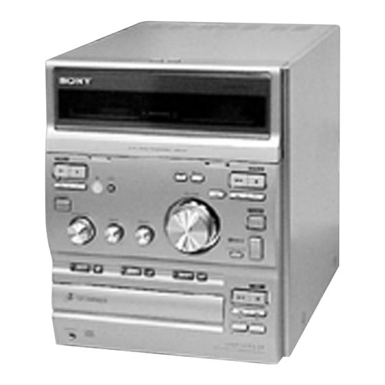
SERVICE MANUAL
Ver 1.1 2003. 11
• HCD-CP333 is the Amplifier, CD player,
Tape Deck and Tuner section in
CMT-CP333.
Amplifier section
For the U.S. model
AUDIO POWER SPECIFICATIONS
POWER OUTPUT AND TOTAL
HARMONIC DISTORTION:
With 6-ohm loads, both channels driven, from
120 - 10,000 Hz; rated 40 watts per channel
minimum RMS power, with no more than 10%
total harmonic distortion from 250 milliwatts to
rated output.
North American model
Continuous RMS power output (reference):
40 + 40 W
(6 ohms at 1 kHz, 10%
THD)
Total harmonic distortion less than 0.07% (6 ohms at
1 kHz, 32 W)
European model
DIN power output (rated): 32 + 32 W
(6 ohms at 1 kHz, DIN)
Continuous RMS power output (reference):
40 + 40 W
(6 ohms at 1 kHz, 10%
THD)
Music power output (reference):
100 + 100 W
Other models
The following measured at 230 V AC, 60 Hz
DIN power output (rated): 30 + 30 W
(6 ohms at 1 kHz, DIN)
Sony Corporation
9-877-051-02
2003K16-1
Home Audio Company
© 2003.11
Published by Sony Engineering Corporation
HCD-CP333
Model Name Using Similar Mechanism
CD
CD Mechanism Type
Section
Optical Pick-up Type
Model Name Using Similar Mechanism
Tape deck
Section
Tape Transport Mechanism Type
SPECIFICATIONS
Continuous RMS power output (reference):
38 + 38 W
(6 ohms at 1 kHz, 10%
THD)
The following measured at 220 V AC, 60 Hz
DIN power output (rated): 27 + 27 W
(6 ohms at 1 kHz, DIN)
Continuous RMS power output (reference):
35 + 35 W
(6 ohms at 1 kHz, 10%
THD)
Inputs
AUDIO IN MD (VIDEO) (phono jacks):
Sensitivity 500/250 mV,
impedance 47 kilohms
Outputs
CD DIGITAL OUT OPTICAL:
Optical
PHONES:
Accepts headphones with
an impedance of 8 ohms
or more
SPEAKER:
6 ohms
CD player section
System
Compact disc and digital
audio system
MICRO HI-FI COMPONENT SYSTEM
US Model
Canadian Model
AEP Model
UK Model
E Model
HCD-CP300
CDM63K-K6BD44
KSM-213D
HCD-CP300
CMBL6Z511A
Laser
Semiconductor laser
(λ = 780 nm)
Emission
duration: continuous
Wavelength
780 - 790 nm
Frequency response
20 Hz - 20 kHz (±0.5 dB)
Tape player section
Recording system
4-track 2-channel stereo
Frequency response
50 - 13,000 Hz (±3 dB),
using a Sony TYPE I
cassette
Tuner section
FM stereo, FM/AM superheterodyne tuner
FM tuner section
Tuning range
North American model:
87.5 - 108.0 MHz
(100-kHz step)
Other models:
87.5 - 108.0 MHz
(50-kHz step)
Antenna
FM wire antenna
Antenna terminals
75 ohm unbalanced
Intermediate frequency
10.7 MHz
— Continued on next page —
Advertisement
Table of Contents

Related Manuals for Sony HCD-CP333


Summary of Contents for Sony HCD-CP333
- Page 1 SERVICE MANUAL US Model Canadian Model Ver 1.1 2003. 11 AEP Model UK Model E Model • HCD-CP333 is the Amplifier, CD player, Tape Deck and Tuner section in CMT-CP333. Model Name Using Similar Mechanism HCD-CP300 CD Mechanism Type CDM63K-K6BD44...
-
Page 2: Table Of Contents
HCD-CP333 Ver 1.1 2003.11 TABLE OF CONTENTS 1. SERVICING NOTES AM tuner section ························································· 4 Tuning range North American model: 530 - 1,710 kHz 2. GENERAL ············································································ 5 (with the tuning interval set at 10 kHz) 531 - 1,710 kHz 3. -
Page 3: Leakage Test
CRITIQUES POUR LA SÉCURITÉ DE FONCTIONNEMENT. NE COMPONENTS WITH SONY PARTS WHOSE PART NUMBERS REMPLACER CES COMPOSANTS QUE PAR DES PIÈSES SONY APPEAR AS SHOWN IN THIS MANUAL OR IN SUPPLEMENTS DONT LES NUMÉROS SONT DONNÉS DANS CE MANUEL OU PUBLISHED BY SONY. -
Page 4: Servicing Notes
HCD-CP333 SECTION 1 SERVICING NOTES SERVICE POSTION NOTES ON HANDLING THE OPTICAL PICK-UP In checking the CD block, prepare jig (extension cable J-2501-011- BLOCK OR BASE UNIT The laser diode in the optical pick-up block may suffer electrostatic break-down because of the potential difference generated by the charged electrostatic load, etc. -
Page 5: General
HCD-CP333 SECTION 2 GENERAL This section is extracted from instruction manual. Main unit 1234 5~6 > wd~wk 1 DISC indicator wa DECK A EJECT Z 5 TAPE A m/M ef BASS ea DECK B EJECT Z 6 TAPE B m/M qs... -
Page 6: Remote Control
HCD-CP333 Remote Control 1 2 3 4 wf~wh w;~wa qgqf BASS/TREBLE ql PLAY MODE wl BUTTON DESCRIPTIONS CD wj SLEEP 1 N wd DIRECTION qj STEREO/MONO qd DISC1 wf TAPE A/B wk DISC2 wg TIMER SELECT 2 . ws DISC3 wh TIMER SET 3 >... -
Page 7: Disassembly
HCD-CP333 Ver 1.1 2003.11 SECTION 3 DISASSEMBLY • The equipment can be removed using the following procedure. COVER (UPPER) FRONT PANEL SECTION TAPE MECHANISM DECK-1 TAPE MECHANISM DECK-2 LED BOARD, CONTROL BOARD BACK PANEL SUB ASSY, JACK BOARD MAIN BOARD... -
Page 8: Cover (Upper)
HCD-CP333 Note : Follow the disassembly procedure in the numerical order given. 3-1. Cover (Upper) 1 six screws (+BTP 3 × 8) 4 cover (upper) 3 two case screws 2 two case screws 3-2. Front Panel Section 7 wire (flat type) 15p (CN805) -
Page 9: Tape Mechanism Deck-1
HCD-CP333 3-3. Tape Mechanism Deck-1 6 tape machanism deck 1 two screws (+BVTP 3 × 8) 2 three screws (+BVTP 3 × 8) 3-4. Tape Mechanism Deck-2 qd wire (flat type) 11p qg two dampers qh tape machanism deck qf two screws (+BVTTWH tapping) -
Page 10: Led Board, Control Board
HCD-CP333 3-5. LED Board, CONTROL Board 9 CONTROL board 6 shield sheet 7 w ire (flat type) 15p (CN807) 8 w ire (flat type) 17p (CN808) 1 four knobs 5 eleven screws (IT3B 2.6 × 8) 3 four screws (IT3B 2.6 × 8) -
Page 11: Main Board
HCD-CP333 3-7. MAIN Board 1 connector 9p (CN902) 5 screw (+BVTP 3 × 12) 6 MAIN board 2 connector 12p (CN313) 4 screw (+BVTP 3 × 8) 3 wire (flat type) 21p (CN304) 3-8. POWER Board 5 POWER board 4 four screws (+BVTP 4 × 8) -
Page 12: Cd Mechanism Deck (Cdm63K-K6Bd44)
HCD-CP333 3-9. CD Mechanism Deck (CDM63K-K6BD44) 5 two screws (+BVTP 3 × 8) q; CD machanism deck (CDM63K-K6BD44) 7 connector 12p (CN701) 2 screw (+BVTP 3 × 8) 1 two screws (+KTP 3 × 8) 3 two screws (+BVTP 3 × 8) -
Page 13: Base Unit (Bu-K6Bd44)
HCD-CP333 3-11. Base Unit (BU-K6BD44) 3 coil spring (insulator) 5 two screws (IT3B 2.6 × 8) 4 insulator 2 two screws (+PTPWH 2.6 × 6) 6 two stoppers (BU) 1 screw, froating 3 coil spring (insulator) 7 two coil springs (insulator) -
Page 14: Silder (Loading)
HCD-CP333 3-13. Silder (Loading) 3 two screws (+BTTP M2.6) 2 bracket (retainer) 4 bracket (retainer) 7 two gears (slider) 1 two screws (+BTTP M2.6) 6 two screws (+PTPWH M2.6) 8 slider (loading) 3-14. TRAY SENSOR Board, MOTOR Board 2 two screws (+BTTP M2.6) 4 two screws (+BTTP M2.6) -
Page 15: In Out Sw Board
HCD-CP333 3-15. IN OUT SW Board t wo screws (+BTTP M2.6) stocker assy 1 Rotate the cam, and up the stocker assy at the full. IN OUT SW board 3 c onnector 2p (CN704) 3-16. Stocker Assy 5 stocker assy 2 screw (+BTTP M2.6) -
Page 16: Cd Base Unit Assy, Disc Sensor Board
HCD-CP333 Ver 1.1 2003.11 3-17. CD Base Unit Assy, DISC SENSOR Board 2 CD base unit assy 4 DISC SENSOR board 3 two screws (BTTP M2.6) 1 c onnector 3p (CN705) -
Page 17: Test Mode
HCD-CP333 SECTION 4 TEST MODE [CD Ship Mode] [CD Ship (Memory Clear) Mode] • This mode moves the optical pick-up to the position durable to • Set the CD ship mode and set the default setup when shipped vibration. Use this mode when returning the set to the customer from the factory at the next AC power on. -
Page 18: Electrical Adjustments
HCD-CP333 SECTION 5 ELECTRICAL ADJUSTMENTS Mode: Playback DECK SECTION 0 dB=0.775 V MAIN board Note: Confirm each contents of this section first of all. If the results are SPEAKER terminals (SJ301) test tape not satisfied, do the adjustment. P-4-A63J L-CH... - Page 19 HCD-CP333 CD SECTION Checking Location: – CD BOARD (Conductor Side) – Note: CD Block is basically constructed to operate without adjustment. Use YEDS-18 disc (3-702-101-01) unless otherwise indicated. Use an oscilloscope with more than 10 MΩ impedance. Clean the object lens by an applicator with neutral detergent when the signal level is low than specified value with the following checks.
-
Page 20: Diagrams
HCD-CP333 SECTION 6 DIAGRAMS 6-1. Note For Printed Wiring Boards And Schematic Diagrams Note on Printed Wiring Boards: Note on Schematic Diagram: • X : parts extracted from the component side. • All capacitors are in µF unless otherwise noted. pF: µµF •... -
Page 21: Block Diagrams
HCD-CP333 Ver 1.1 2003.11 6-2. Block Diagrams – TUNER/CD Section – • RCH is omitted due to same as LCH. • Signal Path TUNER : FM UNIT TU-L ST-L : CD ST-R R-CH MAIN SECTION : DIGITAL OUT TUNED TUNED... - Page 22 HCD-CP333 – MAIN Section – INPUT SELECT TONE/VOL CONT IC301 IC101 TU L TUNER TU-L OUT2 POWER SJ301 SECTION • RCH is omitted SPEAKER Q330 • Signal Path MUTE MUTE +12V CD L CONT Q150 CD-L SECTION : PB (DECK A)
-
Page 23: Circuit Boards Location
HCD-CP333 6-3. Circuit Boards Location • WAVEFORMS JACK board POWER board – CD Board – – MAIN Board – IC101 ta IC601 qa (XCOUT) IC101 wh (MDP) (RFAC)(CD Play mode) 2.2 Vp-p 1.1 Vp-p LCD board 3.2Vp-p 7.5 µ s 30.5 µ... -
Page 24: Printed Wiring Board - Cd Board
HCD-CP333 Ver 1.1 2003.11 6-4. Printed Wiring Board – CD Board – • See page 23 for Circuit Boards Location. IC102 (KSM-213D) IC103 IC101 • Semiconductor Location Ref. No. Location D101 IC101 IC102 IC103 Q101 Q102... -
Page 25: Schematic Diagram - Cd Board
HCD-CP333 Ver 1.1 2003.11 6-5. Schematic Diagram – CD Board – • See page 23 for Waveforms. • See page 42, 43 for IC Block Diagrams. R196 2.2k R195 470k R194 100k C146 CN102 C185 C110 R111 0.47 3300p 120k... -
Page 26: Printed Wiring Board - Tc Board
HCD-CP333 6-6. Printed Wiring Board – TC Board – • See page 23 for Circuit Boards Location. IC401 IC402 • Semiconductor Location Ref. No. Location IC401 IC402 Q401 Q402 Q403 Q404 Q405 Q406 Q410 Q413... -
Page 27: Schematic Diagram - Tc Board
HCD-CP333 6-7. Schematic Diagram – TC Board – • See page 23 for Waveforms. • See page 42 for IC Block Diagram. C412 R445 Q413 C411 R455 C436 DTC343TK C414 47 16V R412 R413 R405 1.8k 330k R450 R403 R411 R415 4.7k... -
Page 28: Printed Wiring Board - Main Board
HCD-CP333 6-8. Printed Wiring Board – MAIN Board – • See page 23 for Circuit Boards Location. • Semiconductor IC602 Location Ref. No. Location IC603 D309 D314 D319 D321 D323 Ω 6-16 D350 IC601 D805 IC301 D806 IC604 D807 D808... -
Page 29: Schematic Diagram - Main Board (1/3)
HCD-CP333 6-9. Schematic Diagram – MAIN Board (1/3) – • See page 41 for IC Block Diagrams. EXCEPT E51 C101 IC101 TDA7296 C105 C121 10uF / 50V 4.7uF / 50V Q210 C201 DTC343TK C205 C350 C221 0.01 C333 4.7uF / 25V... -
Page 30: Schematic Diagram - Main Board (2/3)
HCD-CP333 6-10. Schematic Diagram – MAIN Board (2/3) – CN303 Q364 2SA950 C365 Q366 2SA950 R360 R343 Q361 R359 2SA950 R361 R353 4.7k R357 3.3k R345 R358 R356 C373 3.3k 2.2k 1000p R346 Q362 KRC103S R347 Q365 KRC103S Q367 KRC103S... -
Page 31: Schematic Diagram - Main Board (3/3)
HCD-CP333 6-11. Schematic Diagram – MAIN Board (3/3) – • See page 23 for Waveforms. • See page 41 for IC Block Diagrams. • See page 39 for IC Pin Function Description. CN801 R616 C816 R864 R875 Q802 KTA1266Y-AT D805 MTZJ-T-77-4.3B... -
Page 32: Printed Wiring Board - Control Section
HCD-CP333 6-12. Printed Wiring Board – CONTROL Board – • See page 23 for Circuit Boards Location. JR804 IC605 • Semiconductor Location Ref. No. Location D814 D815 D816 D817 D818 STANDBY D820 D823 D828 D829 D830 D831 D833 IC605 Q815... -
Page 33: Schematic Diagram - Control Section
HCD-CP333 6-13. Schematic Diagram – CONTROL Section – S807 S809 S805 S806 S808 S810 R806 R807 R808 R809 R810 1.0k 1.2k 1.8k 2.7k R848 R849 R846 R845 R847 R850 S801 Q809 Q813 Q811 S812 R815 S818 DTC114EKA-T146 DTC114EKA-T146 DTC114EKA-T146 R825... -
Page 34: Printed Wiring Board - Driver Section
HCD-CP333 6-14. Printed Wiring Board – DRIVER Section – • See page 23 for Circuit Boards Location. IC731 IC732 IC733 IC701 MAIN BOARD CN313 (Page 28) IC751... -
Page 35: Schematic Diagram - Driver Section
HCD-CP333 6-15. Schematic Diagram – DRIVER Section – • See page 41 for IC Block Diagram. M721 C721 0.01 CN721 CN702 R731 C731 IC731 RPI-321 R732 IC701 BA6956AN IC732 RPI-321 R734 R733 R702 IC733 RPI-321 C701 R701 R736 R735 CN701... -
Page 36: Printed Wiring Board - Power Board
HCD-CP333 6-16. Printed Wiring Board – POWER Board – • See page 23 for Circuit Boards Location. (CHASSIS) G901 US,CND EXCEPT E51 EXCEPT E51 • Semiconductor Location Ref. No. Location D901 D903 D904 D905 D906 AEP, UK, E51 D907 D908... -
Page 37: Schematic Diagram - Power Board
HCD-CP333 6-17. Schematic Diagram – POWER Board – EXCEPT E51 T901 CN902 FH907 FH908 F904 FH905 FH906 F903 FH910 F905 FH909 D920 R913 10EDB40-TA1B2 4.7k Q902 2SC2785 RY901 T902 D903 D904 10EDB40-TA1B2 10EDB40-TA1B2 D906 D905 10EDB40-TA1B2 10EDB40-TA1B2 JW906 JW914 C927... -
Page 38: Printed Wiring Board - Lcd Section
HCD-CP333 6-18. Printed Wiring Board – LCD Section – • See page 23 for Circuit Boards Location. 6-19. Schematic Diagram – LCD Section – LCD801 CN802 CN804 AUDIO IN MD(VIDEO) R116 C235 C135 J301 0.001 0.001 PJ301 R216 R217 R117 4.7k... -
Page 39: Ic Pin Function Description
HCD-CP333 6-20. IC Pin Function Description • IC601 M30622MGA-A43FP (SYSTEM CONTROLLER) (MAIN Board) Pin No. Pin Name Description LCD REQ Signal output. LCD command select signal output. AC CUT AC CUT check signal. “L”:ON,”H”:OFF REMOCON Sircs remote control signal input. - Page 40 HCD-CP333 Pin No. Pin Name Description X-RST CD reset signal output. AMP-MUTE AMS signal output. “L”:IN,”H”:OUT. B/L CON Back light LED control signal output. AU-MUTE Audio mute signal output. “H”:IN,”L”:OUT. STBY ON Standby relay ON/OFF signal output. VOL CLK VOL CLK signal output.
-
Page 41: Ic Block Diagrams
HCD-CP333 6-21. IC Block Diagrams IC101, 201 TDA7296 (MAIN Board) THERMAL BIPOLAR SHUTDOWN TRANSCONDACTANCE INPUT STAGE SHORT MOS GAIN & – LEVEL SHIFTING OUTPUT CIRCUIT STAGE STAGE PROTECTION STANDBY/ MUTE BOOST- STRAP 14 15 IC603 BU1924AF (MAIN Board) CLOCK TEST... - Page 42 HCD-CP333 IC401 TA8189N (TC Board) METAL TAPE A CH2/A-L CH2/B-L NF-L OUT-L OUT-L /TAPE B OUT-L NF-L IN-L – – VREF1 IREF VREF2 – – CH1/A-R CH1/B-R NF-R METAL GND1 NF-R OUT-R OUT-R OUT-R IN-R IC101 CXD3017Q (CD Board) 59 58 57...
- Page 43 HCD-CP333 IC102 BA5974FP (CD Board) MUTE INTERFACE LEVEL SHIFT THERMAL SHUTDOWN INTERFACE INTERFACE IC103 CXA2581N (CD Board) APC-OFF (Hi-Z) RW/ROM (H/L) VOFST – – VOFST VOFST DVCC – – – – EQ ON/OFF DVCC DVCC DVCC – – – –...
-
Page 44: Exploded Views
HCD-CP333 SECTION 7 EXPLODED VIEWS NOTE: • -XX, -X mean standardized parts, so they may • The mechanical parts with no reference number The components identified by mark 0 or have some differences from the original one. in the exploded views are not supplied. -
Page 45: Front Panel Section
HCD-CP333 7-2. Front Panel Section not supplied supplied supplied 73 74 supplied supplied Inclueded in No.64 Ref. No. Part No. Description Remarks Ref. No. Part No. Description Remarks 4-232-441-01 KNOB (VOL) 4-233-478-01 BRACKET (CD LID) 4-226-047-01 NUT, HEXAGON 4-233-490-01 SPRING (LID) -
Page 46: Chassis Section
HCD-CP333 7-3. Chassis Section F905 F903 not supplied F902 F901 not supplied not supplied F904 T902 CD mechanism deck not supplied not supplied not supplied Ref. No. Part No. Description Remarks Ref. No. Part No. Description Remarks A-4732-474-A MAIN BOARD, COMPLETE (AEP,UK) 0 F904 1-576-375-11 FUSE, GLASS TUBE (3.15A/125V) (US,CND) -
Page 47: Cd Mechanism Deck-1
HCD-CP333 7-4. CD Mechanism Deck-1 supplied supplied supplied supplied KSM-213DCP/Z-NP supplied Ref. No. Part No. Description Remarks Ref. No. Part No. Description Remarks 4-228-980-01 SPRING (STOCKER), LEAF 4-227-549-11 INSULATOR 4-228-964-01 SLIDER (STOCKER.R) 4-227-045-11 SPRING (INSULATOR), COIL 4-234-423-01 SPRING (STOCKER L), LEAF... -
Page 48: Cd Mechanism Deck-2
HCD-CP333 7-5. CD Mechanism Deck-2 supplied not supplied supplied supplied M721 supplied not supplied Ref. No. Part No. Description Remarks Ref. No. Part No. Description Remarks 4-229-003-01 PULLEY 1-678-457-11 TRAY SENSOR BOARD 4-228-998-01 GEAR (DETECTION) 4-228-988-01 CHASSIS 4-218-253-31 SCREW (M2.6), +BTTP 1-678-460-11 DRIVER BOARD 4-218-253-41 SCREW (M2.6), +BTTP... -
Page 49: Ksm-213D
HCD-CP333 Ver 1.1 2003.11 7-6. KSM-213D Ref. No. Part No. Description Remarks 0 601 A-4735-357-A BASE ASSY, OP (KSM-213D) The components identified by Les composants identifiés par mark 0 or dotted line with mark une marque 0 sont critiques 0 are critical for safety. -
Page 50: Electrical Parts List
HCD-CP333 SECTION 8 ELECTRICAL PARTS LIST NOTE: • Due to standardization, replacements in the • RESISTORS • Abbreviation parts list may be different from the parts All resistors are in ohms. CND : Canadian model specified in the diagrams or the components... - Page 51 HCD-CP333 CONTROL Ref. No. Part No. Description Remarks Ref. No. Part No. Description Remarks R107 1-216-833-11 METAL CHIP 1/16W < CONNECTOR > R108 1-216-827-11 METAL CHIP 3.3K 1/16W (US,CND) CN807 1-568-834-11 SOCKET, CONNECTOR 15P R109 1-216-857-11 METAL CHIP 1/16W * CN808...
- Page 52 HCD-CP333 CONTROL DISK SENSOR DRIVER HEAD PHONE IN OUT SW Ref. No. Part No. Description Remarks Ref. No. Part No. Description Remarks R821 1-216-833-11 METAL CHIP 1/16W 1-678-463-11 DISK SENSOR BOARD R822 1-216-814-11 METAL CHIP 1/16W ****************** R823 1-216-815-11 METAL CHIP...
- Page 53 HCD-CP333 JACK MAIN Ref. No. Part No. Description Remarks Ref. No. Part No. Description Remarks 1-687-871-11 JACK BOARD R845 1-216-819-11 METAL CHIP 1/16W R846 1-216-819-11 METAL CHIP 1/16W *********** R847 1-216-819-11 METAL CHIP 1/16W < CONNECTOR > R848 1-216-819-11 METAL CHIP...
- Page 54 HCD-CP333 MAIN Ref. No. Part No. Description Remarks Ref. No. Part No. Description Remarks C132 1-104-665-11 ELECT 100uF 20.00% 16V C321 1-107-826-11 CERAMIC CHIP 0.1uF 10.00% 16V C133 1-130-495-00 MYLAR 0.1uF C322 1-104-665-11 ELECT 100uF 20.00% 16V C150 1-162-927-11 CERAMIC CHIP...
- Page 55 HCD-CP333 MAIN Ref. No. Part No. Description Remarks Ref. No. Part No. Description Remarks C815 1-162-970-11 CERAMIC CHIP 0.01uF IC305 8-759-584-40 IC KA7908 (AEP,UK) IC308 8-749-016-00 IC HVE0024 (CD DIGITAL OUT OPTICAL) C816 1-126-947-11 ELECT 47uF 20.00% 16V IC311 8-759-646-54 IC KIA7808API...
- Page 56 HCD-CP333 MAIN Ref. No. Part No. Description Remarks Ref. No. Part No. Description Remarks R106 1-216-833-11 METAL CHIP 1/16W R359 1-216-841-11 METAL CHIP 1/16W R360 1-216-841-11 METAL CHIP 1/16W R107 1-216-832-11 METAL CHIP 8.2K 1/16W R361 1-216-841-11 METAL CHIP 1/16W...
- Page 57 HCD-CP333 MAIN MOTOR POWER Ref. No. Part No. Description Remarks Ref. No. Part No. Description Remarks R649 1-216-821-11 METAL CHIP 1/16W R865 1-216-841-11 METAL CHIP 1/16W R650 1-216-821-11 METAL CHIP 1/16W (AEP,UK) R651 1-216-821-11 METAL CHIP 1/16W R866 1-216-809-11 METAL CHIP...
- Page 58 HCD-CP333 POWER Ref. No. Part No. Description Remarks Ref. No. Part No. Description Remarks < CONNECTOR > A-2007-972-A TC BOARD, COMPLETE ******************* CN901 1-564-321-00 PIN, CONNECTOR(3.96mm PITCH)2P CN902 1-766-282-11 PIN, CONNECTOR (PC BOARD) 9P < CAPACITOR > < DIODE >...
- Page 59 HCD-CP333 Ver 1.1 2003.11 TRAY SENSOR Ref. No. Part No. Description Remarks Ref. No. Part No. Description Remarks < RESISTOR > 1-678-457-11 TRAY SENSOR BOARD ****************** R401 1-216-821-11 METAL CHIP 1/16W R402 1-216-821-11 METAL CHIP 1/16W < CAPACITOR > R403...
- Page 60 HCD-CP333 REVISION HISTORY Clicking the version allows you to jump to the revised page. Also, clicking the version at the upper right on the revised page allows you to jump to the next revised page. Ver. Date Description of Revision 2003.02...