Table of Contents
Advertisement
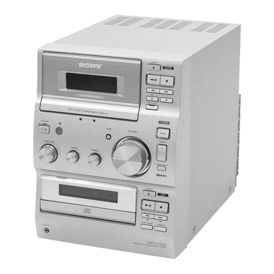
HCD-CP100/CP100K
SERVICE MANUAL
Ver 1.2 2003.07
HCD-CP100/CP100K is the Amplifier, CD
player, Tape Deck and Tuner section in
CMT-CP100/CP100K.
Amplifier section
For the U.S. model
AUDIO POWER SPECIFICATIONS
POWER OUTPUT AND TOTAL
HARMONIC DISTORTION:
With 6-ohm loads, both channels driven, from
70 - 20,000 Hz; rated 18 watts per channel
minimum RMS power, with no more than 0.9%
total harmonic distortion from 250 milliwatts to
rated output.
North American model:
Continuous RMS power output (reference):
Total harmonic distortion less than 0.07% (6 ohms at
1 kHz, 18 W)
European model:
DIN power output (rated): 30 + 30 W
Continuous RMS power output (reference):
Music power output (reference):
Sony Corporation
9-873-803-13
2003G05-1
Home Audio Company
C 2003.07
Published by Sony Engineering Corporation
CD
Section
Tape deck
Section
SPECIFICATIONS
Other models:
The following measured at 230 V AC, 60 Hz
DIN power output (rated): 27 + 27 W
Continuous RMS power output (reference):
The following measured at 220 V AC, 60 Hz
DIN power output (rated): 23 + 23 W
Continuous RMS power output (reference):
Inputs
AUDIO IN MD (VIDEO) (phono jacks):
35 + 35 W
(6 ohms at 1 kHz, 10%
THD)
Outputs
OPTICAL DIGITAL OUT (CD):
PHONES (stereo phone jack):
(6 ohms at 1 kHz, DIN)
SPEAKER:
35 + 35 W
(6 ohms at 1 kHz, 10%
THD)
85 + 85 W
MICRO Hi-Fi COMPONENT SYSTEM
Canadian Model
Australian Model
Model Name Using Similar Mechanism
CD Mechanism Type
Base Unit Name
Optical Pick-up Block Name
Optical Pick-up Name
Model Name Using Similar Mechanism
(6 ohms at 1 kHz, DIN)
32 + 32 W
(6 ohms at 1 kHz, 10%
THD)
(6 ohms at 1 kHz, DIN)
26 + 26 W
(6 ohms at 1 kHz, 10%
THD)
Sensitivity 500/250 mV,
impedance 47 kilohms
Optical
Accepts headphones with
an impedance of 8 ohms
or more
Active speaker system,
6 ohms
US Model
AEP Model
UK Model
HCD-CP100
E Model
HCD-CP100/CP100K
NEW
CDM55F-K6BD41A
BU-K6BD41A
KSM-213DCP
KSS-213D
NEW
– Continued on next page –
Advertisement
Table of Contents

Related Manuals for Sony HCD-CP100


Summary of Contents for Sony HCD-CP100
- Page 1 Canadian Model Ver 1.2 2003.07 AEP Model UK Model Australian Model HCD-CP100 E Model HCD-CP100/CP100K HCD-CP100/CP100K is the Amplifier, CD player, Tape Deck and Tuner section in CMT-CP100/CP100K. Model Name Using Similar Mechanism CD Mechanism Type CDM55F-K6BD41A Base Unit Name BU-K6BD41A...
-
Page 2: Table Of Contents
Recording system 4-track 2-channel stereo 3-1. Disassembly Flow ............7 Frequency response 50 - 13,000 Hz (±3 dB), using a Sony TYPE I 3-2. Cover (Upper) ..............8 cassette 3-3. CD Lid ................8 ±0.15% W. Peak (IEC) Wow and flutter 3-4. -
Page 3: Leakage Test
OPERATION. REPLACE THESE COMPONENTS WITH DE FONCTIONNEMENT. NE REMPLACER CES COM- SONY PARTS WHOSE PART NUMBERS APPEAR AS POSANTS QUE PAR DES PIÈCES SONY DONT LES SHOWN IN THIS MANUAL OR IN SUPPLEMENTS PUB- NUMÉROS SONT DONNÉS DANS CE MANUEL OU LISHED BY SONY. -
Page 4: Servicing Notes
HCD-CP100/CP100K SECTION 1 SERVICING NOTES SERVICE POSTION NOTES ON HANDLING THE OPTICAL PICK-UP In checking the CD block, prepare jig (extension cable J-2501- BLOCK OR BASE UNIT 011-B). The laser diode in the optical pick-up block may suffer electro- static break-down because of the potential difference generated by the charged electrostatic load, etc. -
Page 5: Location Of Controls
HCD-CP100/CP100K SECTION 2 GENERAL • LOCATION OF CONTROLS – Front View – 1 STANDBY I/1 button and indicator 2 Remote sensor 3 BASS knob 4 TREBLE knob 5 DSG button and indicator 6 TAPE REC z button 7 TAPE Y button... -
Page 6: Setting The Time
HCD-CP100/CP100K This section is extracted from instruction manual. Remote Control 1 DSG button qs TIMER SELECT button 1 2 3 2 DISPLAY button qd ENTER button 3 I/1 (power) button qf SLEEP button 4 X button qg TIMER SET button... -
Page 7: Disassembly
HCD-CP100/CP100K SECTION 3 DISASSEMBLY • This set can be disassembled in the order shown below. 3-1. DISASSEMBLY FLOW 3-2. COVER (UPPER) (Page 8) 3-3. CD LID (Page 8) 3-4. FRONT PANEL SECTION (Page 9) 3-6. CD MECHANISM DECK 3-5. TAPE MECHANISM DECK... -
Page 8: Cover (Upper)
HCD-CP100/CP100K Note: Follow the disassembly procedure in the numerical order given. 3-2. COVER (UPPER) 1 four screws × (BVTP4 3 cover (upper) 2 two case screws 2 two case screws 3-3. CD LID 2 CD lid 1 tray Note: Open the tray by supplying the power. -
Page 9: Front Panel Section
HCD-CP100/CP100K 3-4. FRONT PANEL SECTION 1 wire (flat type) 23p 2 connector (CN801) (CN501) 1 wire (flat type) 18p (CN802) 1 wire (flat type) 20p (CN804) 1 wire (flat type) 21p (CN301) 5 front panel section 4 screw (KTP3 × 6) 4 screw (KTP3 ×... -
Page 10: Cd Mechanism Deck (Cdm55F-K6Bd41A)
HCD-CP100/CP100K 3-6. CD MECHANISM DECK (CDM55F-K6BD41A) 2 connector 1 flexible flat cable (19core) (CN401) (CN101) 3 tscrew (BTP3 × 8) 4 CD mechanism deck (CDM55F-K6BD41A) 3-7. BASE UNIT (BU-K6BD41A) 1 floating screw (PTPWHM2.6) 2 base unit (BU-K6BD41A) -
Page 11: Loading Board
HCD-CP100/CP100K 3-8. LOADING BOARD 2 belt (CDM55) 1 Rotate the gear(B) in the direction of arrow A . 3 Pull the tray pushing B . 5 LOADING board 4 two screws (BTP2.6 × 6) 3-9. CAM (CDM55) 3 spacer (55) -
Page 12: Test Mode
HCD-CP100/CP100K SECTION 4 TEST MODE [Cold Reset] [CD Aging Mode] • The cold reset clears all data including preset data stored in the This mode can be used for operation check of CD section. RAM to initial conditions. Execute this mode when returning the set to the customer. -
Page 13: Electrical Adjustments
HCD-CP100/CP100K SECTION 5 ELECTRICAL ADJUSTMENTS Turn the adjustment screw and check output peaks. If the peaks DECK SECTION 0 dB=0.775 V CD SECTION Checking Location: do not match for L-CH and R-CH, turn the adjustment screw Note: Confirm each contents of this section first of all. If the results are so that outputs match within 1dB of peak. -
Page 14: Diagrams
HCD-CP100/CP100K SECTION 6 DIAGRAMS 6-1. BLOCK DIAGRAM – CD SERVO Section – FILTER DIGITAL SIGNAL PROCESSOR, DIGITAL FILTER, D/A CONVERTER OPTICAL IC101 (1/2) 54 56 53 55 PICK-UP BLOCK (KSS-213DCP) OPTICAL DIGITAL D OUT ERROR OPTICAL TRANSCVER RF AMP CORRECTOR... -
Page 15: Block Diagram - Main Section
HCD-CP100/CP100K 6-2. BLOCK DIAGRAM – MAIN Section – R-CH J301 INPUT SELECT SWITCH, HEADPHONE AMP PHONES MIX, TONE CONTROL, IC324 (EXCEPT CP100 : US, CND) ELECTRICAL VOLUME MUTING IC323 SJ301 Q815, 817 ANENNA TUNER PACK SPEAKER IMPEADANCE FM75Ω LINE USE 6 – 16Ω... -
Page 16: Block Diagram - Display/Power Supply Section
HCD-CP100/CP100K 6-3. BLOCK DIAGRAM – DISPLAY/POWER SUPPLY Section – D812 WAKE UP SWITCH Q890, 891 ROTARY RV801 JOG A ENCODER VOLUME JOG B (ROTARY ENCODER) RV801 D811 RESET SIGNAL RESET GENERATOR ROTARY IC803 RV802 JOG E (TREBLE) ENCODER TREBLE JOG F (TREBLE) RV802 D866 –... -
Page 17: Note For Printed Wiring Boards And Schematic Diagrams
HCD-CP100/CP100K 6-4. NOTE FOR PRINTED WIRING BOARDS AND SCHEMATIC DIAGRAMS • Circuit Boards Location Note on Printed Wiring Boards: Note on Schematic Diagram: • All capacitors are in µF unless otherwise noted. pF: µµF • X : parts extracted from the component side. -
Page 18: Printed Wiring Board - Cd Board
HCD-CP100/CP100K 6-5. PRINTED WIRING BOARD – CD Board – • See page 17 for Circuit Boards Location. • Semiconductor Location Ref. No. Location IC101 IC102 IC103 CD BOARD Q101 (SPINDLE) (LIMIT) (SLED) OPTICAL PICK-UP BLOCK (KSM-213DCP) TP (RF) MAIN BOARD... -
Page 19: Schematic Diagram - Cd Board
HCD-CP100/CP100K 6-6. SCHEMATIC DIAGRAM – CD Board – • • See page 25 for Waveforms. See page 32 for IC Block Diagrams. (Page 22) • Voltages and waveforms are dc with respect to ground under no-signal conditions. no mark : CD PLAY ∗... -
Page 20: Printed Wiring Board - Tc Board
HCD-CP100/CP100K 6-7. PRINTED WIRING BOARD – TC Board – • See page 17 for Circuit Boards Location. • Semiconductor Location Ref. No. Location (Page 24) IC401 IC402 MAIN BOARD CASSETTE HOLDER CN301 Q401 BACK LIGHT TC BOARD Q402 Q403 Q406... -
Page 21: Schematic Diagram - Tc Board
HCD-CP100/CP100K 6-8. SCHEMATIC DIAGRAM – TC Board – • • See page 25 for Waveforms. See page 32 for IC Block Diagram. (Page 22) • Voltages and waveforms are dc with respect to ground under no-signal conditions. no mark : PB... -
Page 22: Schematic Diagram - Main (1/2)/Loading Board
HCD-CP100/CP100K 6-9. SCHEMATIC DIAGRAM – MAIN (1/2)/LOADING Board – • See page 32 for IC Block Diagrams. (Page 29) (Page 21) (Page 31) (Page 23) (Page 23) (Page 23) (Page 23) (Page 23) (Page 19) (Page 23) (Page 23) • Voltages and waveforms are dc with respect to ground under no-signal (detuned) conditions. -
Page 23: Schematic Diagram - Main Board (2/2)
HCD-CP100/CP100K 6-10. SCHEMATIC DIAGRAM – MAIN Board (2/2) – • • See page 25 for Waveforms. See page 32 for IC Block Diagram. (Page 29) (Page 29) (Page 22) (Page 27) (Page 22) (Page 22) (Page 22) (Page 22) • Voltages and waveforms are dc with respect to ground... -
Page 24: Printed Wiring Board - Main Board
HCD-CP100/CP100K 6-11. PRINTED WIRING BOARD – MAIN Board – • See page 17 for Circuit Boards Location. • Semiconductor Location Ref. No. Location SWITCH BOARD (Page 26) CN805 MAIN BOARD D303 D304 D305 TUNER PACK SUPPLIED WITH D306 B-10 THE ASSEMBLED BLOCK... - Page 25 HCD-CP100/CP100K • Waveforms – CD Board – – TC Board – – MAIN Board – 1 IC103 qh (RFO) (CD Play Mode) 6 IC101 w; (SCOR) (CD Play Mode) 1 ERASE Head (REC Mode) 1 IC801 el (EXTAL1) 1.2 ±0.1 Vp-p 5.4 Vp-p...
-
Page 26: Printed Wiring Boards - Switch/Tc Switch/Prism Boards
HCD-CP100/CP100K 6-12. PRINTED WIRING BOARDS – SWITCH/TC SWITCH/PRISM Boards – • See page 17 for Circuit Boards Location. • Semiconductor Location Ref. No. Location SWITCH BOARD D851 D852 D853 D854 D855 D856 D857 D858 D859 TUNER IC802 Q851 Q852 BAND... -
Page 27: Schematic Diagram - Switch/Tc Switch/Prism Boards
HCD-CP100/CP100K 6-13. SCHEMATIC DIAGRAM – SWITCH/TC SWITCH/PRISM Boards – (Page 23) • Voltages and waveforms are dc with respect to ground under no-signal (detuned) conditions. no mark : FM... -
Page 28: Ic Pin Function Description
HCD-CP100/CP100K 6-14. IC PIN FUNCTION DESCRIPTION • MAIN BOARD IC801 CXP83124A-048Q (SYSTEM CONTROLLER, LCD DRIVER) Pin No. Pin Name Description Pin No. Pin Name Description TAPE-END Tape end detect sensor input terminal “H” input when the tape end detected JOG-F... -
Page 29: Printed Wiring Boards - Lcd/Headphone Boards
HCD-CP100/CP100K 6-15. PRINTED WIRING BOARDS – LCD/HEADPHONE Boards – 6-16. SCHEMATIC DIAGRAM – LCD/HEADPHONE Boards – • See page 17 for Circuit Boards Location. LCD BOARD BACK BACK LIGHT LIGHT LIQUID CRYSTAL DISPLAY 1-680-956- (11) (Page 23) (Page 23) MAIN BOARD... -
Page 30: Printed Wiring Board - Power Board
HCD-CP100/CP100K 6-17. PRINTED WIRING BOARD – POWER Board – • See page 17 for Circuit Boards Location. • Semiconductor Location Ref. No. Location POWER BOARD D902 D903 D904 D905 D906 D907 D908 D909 D910 D911 D912 D913 D915 D917 D918... -
Page 31: Schematic Diagram - Power Board
HCD-CP100/CP100K 6-18. SCHEMATIC DIAGRAM – POWER Board – (Page 22) • Voltages and waveforms are dc with respect to ground The components identified by mark 0 or dotted under no-signal (detuned) conditions. line with mark 0 are critical for safety. - Page 32 HCD-CP100/CP100K • IC Block Diagrams – CD Board – IC101 CXD2587Q IC103 CXA2568M-T6 HOLD APC PD AMP LC/PD ERROR DIGITAL APC LD AMP CORRECTOR – LD ON DIGITAL ASYMMETRY CORRECTION – OPERATIONAL LRCK AMPLIFIER ANALOG SWITCH – PCMD INTERFACE DEMODULATOR –...
-
Page 33: Main Board
HCD-CP100/CP100K – TC Board – IC401 TA8189N METAL TAPE A CH2/A CH2/B /TAPE B – – VREF1 IREF VREF2 – – CH1/A CH1/B METAL GND1 – MAIN Board – IC101, 201 TDA7296 IC320 KA3082 THERMAL BIPOLAR DRIVER OUT SHUTDOWN TRANSCONDACTANCE INPUT STAGE MOS GAIN &... - Page 34 HCD-CP100/CP100K IC804 BU1924F-E2 12 11 10 CLOCK TEST PLL 57kHz RDS/ARI 1187.5Hz COMPARATOR 8th SWITCHED BIPHASE CAPACITOR DECODER FILTER DEFFERENTIAL ANTI-ALIASING DECODER FILTER...
-
Page 35: Exploded Views
HCD-CP100/CP100K SECTION 7 EXPLODED VIEWS NOTE: • -XX and -X mean standardized parts, so they • Items marked “*” are not stocked since they The components identified by mark 0 or dotted line with mark may have some difference from the original are seldom required for routine service. -
Page 36: Front Panel Section
HCD-CP100/CP100K 7-2. FRONT PANEL SECTION supplied not supplied not supplied Ref. No. Part No. Description Remark Ref. No. Part No. Description Remark 4-232-471-01 WINDOW, CD A-4726-170-A SWITCH BOARD, COMPLETE 4-232-478-01 FOOT (CP100: TH/CP100K) 4-232-441-01 KNOB (VOL) 1-757-805-11 WIRE (FLAT TYPE) 23P... -
Page 37: Chassis Section
HCD-CP100/CP100K 7-3. CHASSIS SECTION not supplied E, EA, AR, SP, AUS CDM55F-K6BD41A not supplied not supplied The components identified by mark 0 or dotted line with mark 0 are critical for safety. Replace only with part number specified. Les composants identifiés par une marque 0 sont critiquens pour la sécurité. -
Page 38: Cd Mechanism Deck (Cdm55F-K6Bd41A)
HCD-CP100/CP100K 7-4. CD MECHANISM DECK (CDM55F-K6BD41A) M901 BU-K6BD41A Ref. No. Part No. Description Remark Ref. No. Part No. Description Remark 4-224-894-01 TRAY 4-221-815-02 ROLLER 4-220-229-02 LEVER (SW) 4-231-779-01 CHASSIS (F) 4-220-239-01 SPRING, TORSION A-4735-081-A PULLEY (AT-55F) ASSY 4-221-816-01 BELT (CDM55) -
Page 39: Base Unit (Bu-K6Bd41A)
HCD-CP100/CP100K Ver 1.2 7-5. BASE UNIT (BU-K6BD41A) The components identified by Les composants identifiés par une mark 0 or dotted line with marque 0 sont critiques pour la mark 0 are critical for safety. sécurité. Replace only with part num- Ne les remplacer que par une pièce... -
Page 40: Electrical Parts List
HCD-CP100/CP100K SECTION 8 ELECTRICAL PARTS LIST NOTE: • Due to standardization, replacements in the • Items marked “*” are not stocked since they The components identified by 0 or dotted line with mark mark parts list may be different from the parts speci- are seldom required for routine service. - Page 41 HCD-CP100/CP100K Ver 1.1 HEADPHONE LOADING MAIN Ref. No. Part No. Description Remark Ref. No. Part No. Description Remark 1-680-956-11 LCD BOARD R118 1-216-809-11 METAL CHIP 1/16W ********** R119 1-216-817-11 METAL CHIP 1/16W R123 1-216-833-11 METAL CHIP 1/16W < CONNECTOR >...
- Page 42 HCD-CP100/CP100K MAIN Ref. No. Part No. Description Remark Ref. No. Part No. Description Remark C130 1-162-953-11 CERAMIC CHIP 100PF C317 1-164-156-11 CERAMIC CHIP 0.1uF C318 1-104-661-11 ELECT 330uF C140 1-126-961-11 ELECT 2.2uF C141 1-126-965-11 ELECT 22uF C319 1-164-156-11 CERAMIC CHIP 0.1uF...
- Page 43 HCD-CP100/CP100K MAIN Ref. No. Part No. Description Remark Ref. No. Part No. Description Remark C805 1-115-156-11 CERAMIC CHIP < SHORT > C806 1-115-156-11 CERAMIC CHIP JR115 1-216-864-11 SHORT C807 1-107-826-11 CERAMIC CHIP 0.1uF JR215 1-216-864-11 SHORT C808 1-107-826-11 CERAMIC CHIP 0.1uF...
- Page 44 HCD-CP100/CP100K MAIN Ref. No. Part No. Description Remark Ref. No. Part No. Description Remark Q809 8-729-038-67 TRANSISTOR KRC102S R240 1-216-817-11 METAL CHIP 1/16W Q810 8-729-038-67 TRANSISTOR KRC102S R241 1-216-837-11 METAL CHIP 1/16W R242 1-216-841-11 METAL CHIP 1/16W Q811 8-729-038-67 TRANSISTOR...
- Page 45 HCD-CP100/CP100K MAIN Ref. No. Part No. Description Remark Ref. No. Part No. Description Remark R801 1-216-821-11 METAL CHIP 1/16W R853 1-216-829-11 METAL CHIP 4.7K 1/16W R854 1-216-829-11 METAL CHIP 4.7K 1/16W R802 1-216-821-11 METAL CHIP 1/16W R855 1-216-829-11 METAL CHIP 4.7K...
- Page 46 HCD-CP100/CP100K MAIN POWER Ref. No. Part No. Description Remark Ref. No. Part No. Description Remark < TUNER UNIT > D912 8-719-991-33 DIODE 1SS133T-77 D913 8-719-991-33 DIODE 1SS133T-77 A-4476-412-A TUNER UNIT (TCB-022N) D915 8-719-109-93 DIODE MTZJ-T-77-6.2B (EXCEPT CP100: AEP, UK, AUS)
- Page 47 HCD-CP100/CP100K POWER PRISM SWITCH Ref. No. Part No. Description Remark Ref. No. Part No. Description Remark 0 T902 1-437-250-11 TRANSFORMER, POWER R651 1-216-836-11 METAL CHIP 1/16W (CP100: E, EA, SP, AR, TW, BR, HK) R652 1-216-831-11 METAL CHIP 6.8K 1/16W...
- Page 48 HCD-CP100/CP100K TC SWITCH Ref. No. Part No. Description Remark Ref. No. Part No. Description Remark < CAPACITOR > R405 1-216-809-11 METAL CHIP 1/16W R406 1-216-831-11 METAL CHIP 6.8K 1/16W C402 1-162-962-11 CERAMIC CHIP 470PF C403 1-104-509-11 CERAMIC CHIP 0.018uF R407...
- Page 49 HCD-CP100/CP100K Ver 1.2 TC SWITCH Ref. No. Part No. Description Remark Ref. No. Part No. Description Remark < TRANSISTOR > ACCESSORIES ************ Q853 8-729-038-67 TRANSISTOR KRC102S 1-770-019-11 ADAPTOR, CONVERSION PLUG 3P < RESISTOR > (CP100: UK) R659 1-216-829-11 METAL CHIP 4.7K...
-
Page 50: Revision History
HCD-CP100/CP100K REVISION HISTORY Clicking the version allows you to jump to the revised page. Also, clicking the version at the upper right on the revised page allows you to jump to the next revised page. Ver. Date Description of Revision 2001.02...