Advertisement
Table of Contents
- 1 Table of Contents
- 2 Chapter 1. Specifications
- 3 CHR. the Lamp Lights up When Character Key Sheet Mode in
- 4 Chapter 2. Options
- 5 Chapter 3. Srv. Reset and Master Reset
- 6 Chapter 4. Hardware Description
- 7 Chapter 5. Test Function
- 8 Chapter 6. Download Function
- 9 Chapter 7. Circuit Diagram & Pwb Layout
- 10 Parts Guide
- Download this manual
See also:
Programming Manual
ER-A460
CAUTION
EXTREME CAUTION MUST BE TAKEN WHEN SERVICING THIS MACHINE. EVEN
THOUGH THE MODE SWITCH IS IN THE OFF POSITION, VOLTAGE IS STILL SUPPLIED
TO THE ENTIRE MACHINE.
WHEN WORKING ON THIS MACHINE MAKE SURE THAT THE POWER CORD IS
REMOVED FROM THE WALL OUTLET.
CHAPTER 1. SPECIFICATIONS . . . . . . . . . . . . . . . . . . . . . . . . . . . . . . . . . . . . . 1
CHAPTER 2. OPTIONS . . . . . . . . . . . . . . . . . . . . . . . . . . . . . . . . . . . . . . . . . . . 6
CHAPTER 3. SRV. RESET AND MASTER RESET . . . . . . . . . . . . . . . . . . . . . . 9
CHAPTER 4. HARDWARE DESCRIPTION . . . . . . . . . . . . . . . . . . . . . . . . . . . 10
CHAPTER 5. TEST FUNCTION . . . . . . . . . . . . . . . . . . . . . . . . . . . . . . . . . . . . 32
CHAPTER 6. DOWN LOAD FUNCTION . . . . . . . . . . . . . . . . . . . . . . . . . . . . . . 39
CHAPTER 7. CIRCUIT DIAGRAM & PWB LAYOUT . . . . . . . . . . . . . . . . . . . . 41
Parts marked with "! " is important for maintaining the safety of the set. Be sure to replace these parts with specified ones for
maintaining the safety and performance of the set.
SERVICE MANUAL
ER-A470
CONTENTS
SHARP CORPORATION
CODE: 00ZERA460VSME
ELECTRONIC
CASH REGISTER
ER-A460
MODEL
ER-A470
MODEL
SRV Key : LKGIM7113RCZZ
PRINTER : DP-730
(For "V" version)
This document has been published to be used
for after sales service only.
The contents are subject to change without notice.
Advertisement
Table of Contents

Related Manuals for Sharp ER-A460


Summary of Contents for Sharp ER-A460
-
Page 1: Table Of Contents
SERVICE MANUAL CODE: 00ZERA460VSME ELECTRONIC CASH REGISTER ER-A460 MODEL ER-A460 ER-A470 MODEL SRV Key : LKGIM7113RCZZ PRINTER : DP-730 (For "V" version) ER-A470 CAUTION EXTREME CAUTION MUST BE TAKEN WHEN SERVICING THIS MACHINE. EVEN THOUGH THE MODE SWITCH IS IN THE OFF POSITION, VOLTAGE IS STILL SUPPLIED TO THE ENTIRE MACHINE. -
Page 2: Chapter 1. Specifications
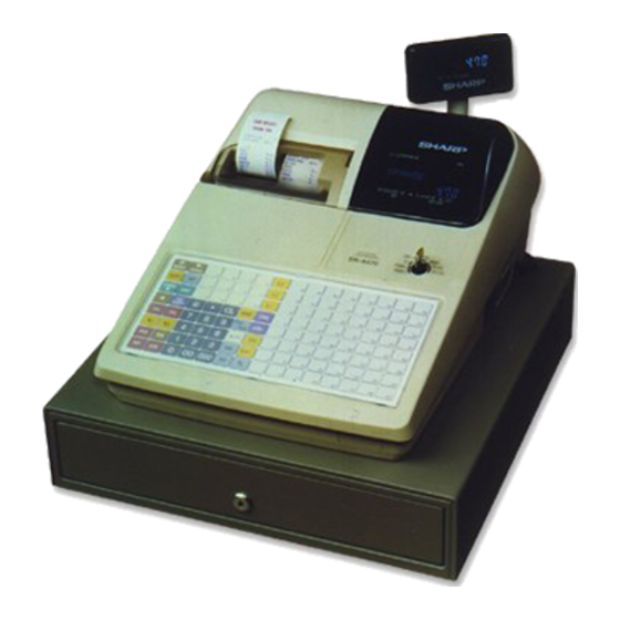
CHAPTER 1. SPECIFICATIONS 1. Appearance/Rating 1) Appearance ER-A460 Infrared sensor Velidation opening Journal window Customer display Printer cover (Pop-up type) Operator display Receipt paper Ribbon cover Mode switch Power switch Keyboard Drawer Drawer lock Printer cover lock * To lock or unlock the drawer, * To lock or unlock the printer cover, use the printer cover lock key. - Page 3 2. Keyboard 1) Standard keyboard layout ER-A460 CASH PLU/SUB AUTO COPY RECEIPT JOURNAL RCPT ER-A470 RECEIPT JOURNAL RCPT CASH COPY PLU/ AUTO Fig. 2-1 – 2 –...
- Page 4 2) Key top name Standard key top Option key top KEY TOP DESCRIPTION KEY TOP DESCRIPTION A460 A470 A460 A470 0 to 9, 00 Numeric keys PLU’s level shift 1 key 000 key PLU’s level shift 2 key ↑ RECEIPT Receipt paper feed key PLU’s level shift 3 key ↑...
-
Page 5: Chr. The Lamp Lights Up When Character Key Sheet Mode In
3. Mode switch Dot display 7 segment display No. of positions Color of display Green Green Character size 6.6 (H) 4.6 (W) mm 10.0 (H) 4.3 (W) mm Customer display OP X/Z X1/Z1 PGM1 X2/Z2 PGM2 (SRV) (SRV') Fig. 4-2 No. - Page 6 • Character size: 2.4 (H) 1.36 (W) mm 3) Paper Print pitch: • Paper roll dimensions: 44.5±0.5mm in width, 83mm in diameter Column distance 1.59 mm • Row distance 5.08 mm Paper quality: Journal Bond paper (paper thickness: 0.06 to •...
-
Page 7: Chapter 2. Options
CHAPTER 2. OPTIONS 1. System configuration – 6 –... - Page 8 E R – 0 1 F D / 0 2 F D PRESETS LOADER FD unit E R – 1 1 K T 7 KEY TOP KIT (For ER-A460) 1 key top E R – 1 2 K T 7 2 key top E R –...
- Page 9 Purpose 1: Used for servicing and repairing of options (such as the and the ER-A5RS) which are connected with the main body option connector. [Procedure 1] Use an insulator base as shown in Fig. 7-2 (shaded section) and perform servicing. ER-A460/A470 Loop back connectors (2 pcs.): UKOG-6705RCZZ Expansion PWB ER-A5RS (CKOG-6708RCZZ)
-
Page 10: Chapter 3. Srv. Reset And Master Reset
[key setup procedure] CHAPTER 3. SRV. RESET AND MASTER RESET MRS-2 Key position set Free key Free key setup executed complete. 1. SRV. reset (Program Loop Reset) Disable Used to return the machine back to its operational state after a lock- up has occurred. -
Page 11: Chapter 4. Hardware Description
CHAPTER 4. HARDWARE DESCRIPTION 1. Hard ware block diagram STANDARD OPTIONAL ER-01RA:32KB RAM1 RAM2 ER-02RA:128KB 32KB MAX.128KB DRAWER MAX.2 STANDARD OPTIONAL GATE ARRAY ER-A46R1 MPCA6 OPERATER DISPLAY 256KB 128KB 2 LINE 5 x 7DOT 12DIG 7SEG 10DIG CUSTOMER DISPLAY 1 LINE 7SEG 7DIG PRINTER DP-730 CKDC6... - Page 12 2. Description of main LSI’s 2-1. CPU (HD6415108FX) 1) Pin configuration AVSS P65/RS P64/RR P63/CD P62/CS P61/DR P60/ER P57/STOP FMRS P50/FTCA1 FTI2 FTI1 TMCI HD6415108FX pin configuration Fig. 2-1 – 11 –...
- Page 13 2) Block diagram P27/A23 P26/A22 Data bus Port 1 P25/A21 P24/A20 P23/A19 P22/A18 P21/A17 P20/A16 EXTAL XTAL Clock Watch oscillator dog timer H8/500 CPU STBY Interruption controller 16bit free running Refresh controller timer x 2ch RFSH BREQ BACK Wait state 8bit timer controller WAIT...
-
Page 14: Printer (Dp
3) Pin description Signal Signal Symbol Function Symbol Function name name RESET Reset input Remote drawer No.2 open signal (NU) Non-maskable interrupt input for SSP interrupt input. Remote drawer No.3 open signal (NU): GND Slip printer (M-240) interface connect signal (NU) TMCi PTMG Printer (DP-730) timing signal... - Page 15 Signal Symbol Function name CKDC Interface shift input RXD2 RXD2 data CKDC Interface shift output TXD2 TXD2 data EXTAL EXTAL Crystal oscillator connection XTAL XTAL Crystal oscillator connection 100 VSS 101 X Out System clock 102 E Out Nu 103 AS Out Address strobe 104 RD Out Read...
- Page 16 2-2. G.A (MPCA6) 1) Pin configuration EXINT0 EXINT1 PCUT EXINT2 FCUT EXINT3 STAMP RA15 SLRS RA16 SLMTD RA17 RA18 EXWAIT POFF WAIT INT1 HTS1 SCK1 STH1 VRESC SLTMG SLRST PHAI SDT7 SDT6 SDT5 TEST SDT4 SDT3 IPLON SDT2 INT4 SDT1 PRST PTMG TRGI...
- Page 17 2) Block diagram A23~A0 IRLON ROS1 ROS2 Address decode RASEL RAS1 SSPRQ SSP comparison register External CS Image BAR. RAS2 Internal CS control RAS3 OPTCS IRTX IRRX I/R Control D0~D7 ASKRX Buffer TXDI SCKI RXDI HTS1 Multiplexer SCK1 serial select STH1 HTS2 SCK2...
- Page 18 3) Pin description Signal Signal Function Function name name Receipt side paper feed solenoid INT3 Interrupt signal (Nu) Journal side paper feed solenoid RXD2 8 bit serial port output to CPU PCUT Printer partial cut signal (NU) TXD2 8 bit serial port input from CPU FCUT Printer auto cut signal (NU) SCK2...
- Page 19 Signal Function name 1) General description 105 DAX2 — The CKDC6 is a 4-bit microcomputer developed for the ER-A460/ 106 MCR1 — A470 and provides functions to control the real-time clock, keys, and 107 MCR2 — displays. The basic functions of the CKDC6 are shown below.
- Page 20 7SEG-DISPLAY 7DIG DOT-DISPLAY 16DIG DOT DISP CONT. M66004FP P2,3 SHEN SRES,DCS,DSCK,DSO ST0~3 HOST POFF CKDC 6 SYSTEM STOP KEX0,1 SRES DECODER DECODER LS138 LS138 CKDCR KEY BOARD BUZZ MAX. 244key CSFR MODR DECODER DECODER LS153 LS153 BUZZER Fig. 2-5 2) Pin assignment PULL −UP PULL −UP RESET...
- Page 21 3. Clock generator 4. Reset (POFF) circuit 1) CPU (HD64151010FX) +24V 1SS133 XTAL 8.2KG 2.7K 2.7K 14.7456MHz (HD64151010FX) 15KG EXTAL /POFF MPCA6 1µ 50V GL393 9.1KG MTZ5.1A 1000P Fig. 3-1 Basic clock is supplied from a 14.7456MHz ceramic oscillator. POFF The CPU contains an oscillation circuit from which the basic clock is internally driven.
- Page 22 • ROM image area: Image is formed in ROM area address C00000H 5. Memory control C07FFFH. This area is identical to IPL ROM area which will beseparately developed. 1) Memory map • RAM image area: Image is formed in RAM area address 1 All range memory map 1D8000H1DFE7FH.
- Page 23 200000H~3FFFFFH IPLON: IPL board detection signal incorporated in the option slot. Note used in the ER-A460/A470. (Not used) * Base signal is for 2M. Access is performed with two ROM chip select signals ROS1 and * Note: RAS1 signal is formed as OR in the image area of 0 page.j ROS2, which decode 512KB address area respectively to (Lower 32KB).
- Page 24 2) SSP register 6. SSP circuit The break address register (BAR) is accessed through direct address 1) Block diagram of FFFF00H~FFFFFFH. Entry number is 32 entry. This is the circuit employed to do the Special Service Preset(SSP). (Block diagram) FFFF00 SSPRQ BAR0 A0~23...
- Page 25 Each BAR is composed of 4 byte address. Bit composition is as follows: A19 A18 A17 A16 A15 A8 A7 Upper bits Intermediate bits Lower bits Enable register EN (bit7) = 1 Enable = 0 Inhibit Don't care for "-----." <...
- Page 26 4) Printer sensor circuit 7. PRINTER control circuit 1)Block diagram Address bus Data RECEIVER PRINTER RJTMG (DP-730) C3198 DRIVER MPCA6 RJRST Fig. 7-1 2) General description of the printer controller The DP-730 is used as the R/J printer. The printer mechanical timing control is made by the CPU through MPCA6.
- Page 27 5) Dot solenoid drive circuit 7) Stamp circuit +24V +24V VRESC STAMP STAMP0 DOT1~DOT4 DOT1 ~DOT4 IC10 MPCA6 DOT5~DOT7 DOT5 ~DOT7 The STAMP0 (the stamp solenoid drive signal from the MPCA6) flows through the driver IC to the solenoid. A +24V voltage is applied to the MPCA6 solenoid.
- Page 28 8. Drawer drive circuit VRESC +24V +24V DRAW0 Drawer DRAW1 solenoid TD62308F R73 4.7K DOSP 1000P Fig. 8-1 The drawer is directly supported by the CPU. No action starts when the power supply is not steady as the output stage of the driver is pulled VP by VRESC signal.
- Page 29 Timing ST 1) Power on/off sequence 12.45ms +24V 778µ S POFF RESET KEX0 KEX1 10µ S 10µ S 10µ S 80µ S KR0~KR3 STOP KR0A KR0B SHEN KR3A KR3B Fig. 9-3 The mode switch in provided with a special return line MODR, apart from the above return lines.
-
Page 30: Power Supply Circuit
<Dot display> 10. Power supply circuit ENST Switching +24V regulator ST0~ST3 (STR2024) Noise filter 19.1µ s "h" th digit display (h+1) th digit display DGn+1 Display off 17.2µ s VCKDC Battery VRAMP D0~D35 "h" th didit display pattern (h+1) th didit display pattern circuit VBAT DC-DC... -
Page 31: Pressed
12. I/R communication circuit • In the ER-A460/A470, infra-red data transmission of the optical communication system is performed. System IRDA REMOTE KEYBOARD 900 ∼ 1050 nm 900 ∼ 950 nm Carrier wave 950 nm 33 ∼ 40 kHz Sub-carrier wave (16 times of baud rate clock) 500 kHz±10%... - Page 32 Reception circuit The infra-red signals which was transmitted from the transmission unit through the air is received by the photo diode, and sent through the two-system circuit to the MPCA6, where they are modulated and inputted to the CPU. Band-pass Hysteresis Amplifier filter...
-
Page 33: Chapter 5. Test Function
SSP test Drawer-1 open and sensor test KEY POSITION CODE ER-A460 (Normal key) 14 x 6 Drawer-2 open and sensor test ↑R ↑J 016 022 028 034 040 046 052 058 064 070 076 082 Display test-2... -
Page 34: Pressed
4 Test termination ER-A460 KEY HARDWARE CODE Change the MODE switch position other than SRV position to 1. STANDARD KEY LAYOUT terminate the test. The test termination message is printed. SUM CHECK DATA = 6F+65+63+00+02+ ⋅⋅⋅⋅⋅ = E61 = 3681 ↑R ↑J 6F... - Page 35 [5] Mode switch test [8] SSP test 1 Key operation 1 Key operation 105 → TL 109 → TL 2 Details of test 2 Functional description If an SSP is programmed, its contents are automatically checked and the result is printed. M O D E S R V DOT DISPLAY:...
-
Page 36: Pressed
[10] Display test-2 2 Details of test 1) Machine to be tested 1 Key operation 116 → TL The following data are transmitted in the ASK format. Transmission data (9600BPS) 00,11,22,33,44,55,66,77,88, Functional description 99,AA,BB,CC,DD,EE,FF The display CGs in CKDC6 are checked. The 256 CGs are grouped into 32 blocks and each 8 characters is displayed on the I / R S E N D... - Page 37 [12] Standard RAM test The following address check is performed further. Check point address = 1C0000H, 1C0001H 1 Key operation 1C0002H, 1C0004H 120 → TL 1C0008H, 1C0010H 2 Functional description 1C0020H, 1C0040H Perform the following check for the standard RAM 32 KByte 1C0080H, 1C0100H SRAM.
- Page 38 3 Check the following items: Dot pulse adjusting method Check the termination printout. 1. Turn power on. 4 Test termination 2. Measure the voltage of the VP line between the fuse F1 and GND. The test terminates after printing the termination printout. Use a digital voltmeter capable of measuring 100mV steps.
- Page 39 [15] Option RAM test [16] Option ROM test 1 Key operation 1 Key operation: 200 → TL 400 → TL 2 Functional description: Memory to be Address area to be RAM NO. A sum check is done for the option ROM (Address hex C80000H #NO.
-
Page 40: Chapter 6. Download Function
13: Memory full error 4) Service reset the receiving ECR. 2. Communication between ECRs 1) The pop-up display of the ER-A460/A470 is equipped with the IR 3. Communication between an ECR and interface. Set the distance between IR interfaces within 75cm. - Page 41 DIP SW2 PC-DOS format RS232c level CCPM format Note: When performing IR communication with the ER-A460/ A470, the baud rate should be set to 19200 bps only. The PC-DOS format cannot be used for the ER-01FD. 5) CE-IR2/IR4 setting 1 CE-IR2 The CE-IR2 is used in the ASK mode only, and requires no setting.
-
Page 42: Chapter 7. Circuit Diagram & Pwb Layout
– 41 –... - Page 43 – 42 –...
- Page 44 – 43 –...
- Page 45 – 44 –...
- Page 46 – 45 –...
- Page 47 – 46 –...
- Page 48 – 47 –...
- Page 49 2. Main PWB layout – 48 –...
- Page 50 – 49 –...
- Page 51 – 50 –...
- Page 52 – 51 –...
- Page 53 8. IR PWB layout LHLDZ6835BHZZ(LED HOLDER) x2 PSLDM6637BHZZ (SHIELD PLATE) PSPAG 6730BHZZ LED2 LED1 SIR320ST3N SIR320ST3N (IR SPACER) VHPPD410PI/-1(PHOTO DIODE) IR COMM SHARP QCNCM7179BHOE 10µF/10V OS (53015-0510) N7460BH-57 – 52 –...
- Page 54 – 53 –...
- Page 55 – 54 –...
- Page 56 – 55 –...