Sign In
Upload
Manuals
Brands
VIA Technologies Manuals
Computer Hardware
SOM-9X35
VIA Technologies SOM-9X35 Manuals
Manuals and User Guides for VIA Technologies SOM-9X35. We have
3
VIA Technologies SOM-9X35 manuals available for free PDF download: Design Manual, User Manual, Quick Manual
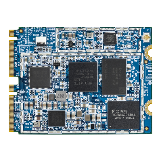
VIA Technologies SOM-9X35 Design Manual (81 pages)
Carrier Board
Brand:
VIA Technologies
| Category:
Control Unit
| Size: 5 MB
Table of Contents
Table of Contents
4
Introduction
10
Document Overview
10
Acronyms Used
11
Table 01: Acronyms Used
11
I/O Parameter Definitions
12
Schematic Conventions
12
Figure 01: Schematic Conventions
12
Table 02: I/O Parameter Definitions
12
General Carrier Board Recommendations
13
PCB Stack-Up
13
Figure 02: Microstrip PCB Stack-Up Example
13
Figure 03: Stripline PCB Stack-Up Example
13
6-Layer PCB Stack-Up Example
14
Impedance Requirements
14
Figure 04: 6-Layer PCB Board Stack-Up Detail
14
Table 03: Impedance Requirements
14
General Layout & Routing Guidelines
15
Figure 05: Point-To-Point and Multi-Drop Examples
15
Figure 06: Daisy-Chain Example
15
Figure 07: Alternate Multi-Drop Example
15
General Trace Attribute Recommendation
16
Figure 08: Single-Ended Trace Width and Spacing Example
16
Figure 09: Differential Trace Width and Spacing Example
16
Table 04: Recommended Trace Width and Spacing
16
General Clock Routing Considerations
17
Figure 10: Suggested Clock Trace Spacing
17
Figure 11: Clock Trace Layout in Relation to the Ground Plane
17
Figure 12: Series Termination for Multiple Clock Loads
17
Trace Bend Geometry
18
Signal Proximity
18
Figure 13: Use 135° Bends Instead of 90
18
Figure 14: Suggested Minimum Distance and Segment Length at Bends
18
Figure 15: Try to Increase Spacing between Traces Whenever It Is Possible
18
Trace Stubs
19
Ground Planes under Pads
19
Figure 16: Avoid Stub Traces by Daisy Chain Routing
19
Figure 17: Remove Ground Plane under Large Pads
19
Differential Pair Signals
20
Length Matching
20
Figure 18: Do Not Put any Components or Vias between Differential Pairs
20
Figure 19: Place Vias Symmetrical
20
Figure 20: Route Pairs on the same Layer, Place same Amount of Vias
20
Figure 21: Route Pairs on the same Layer, Place same Amount of Vias
21
Figure 22: Add Length Correction to the Mismatching Point
21
Figure 23: Place Length Compensation Close to a Bend
21
Figure 24: Length Differences Need to be Compensated in each Segment
22
Figure 25: Pairs Within same Interface Should be Routed Preferable on same Layer
22
Figure 26: Preferred Symmetrical Breakout
22
Figure 27: Preferred Breakout of Differential Pairs
23
SOM-9X35 Module & M.2 Slot Specification Overview
24
SOM-9X35 Module Placement
24
Figure 28: SOM-9X35 Module Placement Example on the Carrier Board
24
SOM-9X35 Module & Carrier Board Dimensions
25
Figure 29: Dimensions of the SOM-9X35 Module
25
Figure 30: Dimensions of the Reference Carrier Board
25
Slot
26
Slot Dimensions
26
Figure 31: Dimensions of the M.2 Slot (Top View)
26
Figure 32: Dimensions of the M.2 Slot (Side View)
26
Table 05: M.2 Slot Sample
26
Slot Height Notes
27
Slot Placement (Unit MM)
27
Slot Pin Assignments
27
Figure 33: M.2 Slot Placement
27
Slot Reference Schematics
37
Figure 34: M.2 Slot Reference Circuitry (Part 1)
37
Table 06: M.2 Slot Pinouts
37
Figure 35: M.2 Slot Reference Circuitry (Part 2)
38
Figure 36: M.2 Slot Reference Circuitry (Part 3)
38
Layout & Routing Recommendation
39
HDMI Interface
39
HDMI Signal Definition
39
Figure 37: HDMI Routing Topology
39
Table 07: HDMI Signal Definition
39
HDMI Layout & Routing Recommendations
40
Figure 38: HDMI Differential Trace Width and Spacing Example
40
Figure 39: HDMI Single-Ended Trace Width and Spacing Example
40
Table 08: HDMI Layout Guidelines
40
HDMI Reference Schematics
41
Figure 40: HDMI Reference Circuitry (Part 1)
41
Table 09: SOM-9X35 HDMI Trace & Via Delay
41
Figure 41: HDMI Reference Circuitry (Part 2)
42
Figure 42: HDMI Reference Circuitry (Part 3)
42
MIPI DSI Interface
43
MIPI DSI Signal Definition
43
Figure 43: MIPI DSI Routing Topology
43
Table 10: MIPI DSI Signal Definition
43
MIPI DSI Layout & Routing Recommendations
44
Figure 44: MIPI DSI Differential Trace Width and Spacing Example
44
Table 11: MIPI DSI Layout Guidelines
44
MIPI DSI Reference Schematics
45
Figure 45: MIPI DSI Reference Circuitry
45
Table 12: SOM-9X35 MIPI DSI Trace & Via Delay
45
LCD Backlight & Bias Voltage Reference Schematics
46
LVDS Interface
46
LVDS Signal Definition
46
Figure 46: LCD Backlight & Bias Voltage Reference Circuitry
46
Figure 47: LVDS Routing Topology
47
Figure 48: LVDS Differential Trace Width and Spacing Example
47
Table 13: LVDS Signal Definition
47
Table 14: LVDS Layout Guidelines
48
Table 15: SOM-9X35 LVDS Trace & Via Delay
48
LVDS Reference Schematics
49
Figure 49: LVDS Reference Circuitry
49
MIPI CSI Interface
50
MIPI CSI Signal Definition
50
Table 16: MIPI CSI0 Signal Definition
50
MIPI CSI Layout & Routing Recommendations
51
Figure 50: MIPI CSI Routing Topology
51
Figure 51: MIPI CSI Differential Trace Width and Spacing Example
51
Table 17: MIPI CSI1 Signal Definition
51
Table 18: MIPI CSI Layout Guidelines
52
Table 19: SOM-9X35 MIPI CSI0 4-Lane Trace & Via Delay
52
Table 20: SOM-9X35 MIPI CSI0A 2-Lane Trace & Via Delay
53
Table 21: SOM-9X35 MIPI CSI0B 2-Lane Trace & Via Delay
53
MIPI CSI Reference Schematics
54
Figure 52: Camera Main Clock Oscillator Reference Circuitry
54
Table 22: SOM-9X35 MIPI CSI1 4-Lane Trace & Via Delay
54
Figure 53: Camera I2C Bus Level Shift Reference Circuitry
55
Figure 54: Camera Control Pin Level Shift Reference Circuitry
55
Figure 55: Camera Power Control Reference Circuitry
56
Figure 56: MIPI 4-Lane Camera Reference Circuitry (Part 1)
56
USB Interface
57
USB Signal Definition
57
Figure 57: MIPI 4-Lane Camera Reference Circuitry (Part 2)
57
Figure 58: USB Routing Topology
57
Table 23: USB Signal Definition
57
USB Layout & Routing Recommendations
58
Figure 59: USB Differential Trace Width and Spacing Example
58
Table 24: USB Layout Guidelines
58
Table 25: USB Port0 OTG
58
Table 26: USB Port0 Host/Device
58
USB Reference Schematics
59
Figure 60: USB Port0 Reference Circuitry
59
Table 27: USB Port0 Trace & Via Delay
59
Table 28: USB Port1 Trace & Via Delay
59
Figure 61: USB Port1 Reference Circuitry (Part1)
60
Figure 62: USB Port1 Reference Circuitry (Part2)
60
SDC Interface
61
SDC Signal Definition
61
SDC Layout & Routing Recommendations
61
Figure 63: SDC Routing Topology
61
Table 29: SDC Signal Definition
61
Figure 64: SDC Single-Ended Trace Width and Spacing Example
62
Table 30: SDC Layout Guidelines
62
Table 31: SOM-9X35 SDC Trace & Via Delay
62
SDC Reference Schematics
63
Analog Audio Interface
63
Analog Audio Signal Definition
63
Figure 65: SDC Reference Circuitry
63
Table 32: Analog Audio Signal Definition
63
PCB Layout Requirement
64
Schematics Requirement
64
Figure 66: Audio Bias Voltage LDO Reference Circuitry
64
Audio Analog Reference Schematics
65
Figure 67: On-Board MIC Reference Circuitry
65
Figure 68: Line-Out & MIC-In Jack Reference Circuitry
65
Figure 69: Speaker Connector Reference Circuitry
66
Figure 70: Class-D Amplifier Reference Circuitry
66
GPIO Interface
67
GPIO Signal Definition
67
Figure 71: GPIO Level Shift Reference Circuitry
67
Table 33: SOM-9X35 GPIO Signal Definition
67
GPIO Extender
68
ADC Interface
68
ADC Signal Definition
68
ADC Design Notes
68
Figure 72: GPIO Expander Reference Circuitry
68
Table 34: SOM-9X35 ADC Signal Definition
68
System Boot Interface
69
System Boot Signal Definition
69
System Boot Design Notes
69
Figure 73: ADC Reference Circuitry
69
Table 35: SOM-9X35 System Boot Signal Definition
69
System Boot Reference Schematics
70
PWM Interface
70
PWM Signal Definition
70
PWM Design Notes
70
Figure 74: SOM-9X35 Power Switch Reference Circuitry
70
Figure 75: SOM-9X35 BATSNS Reference Circuitry
70
Table 36: SOM-9X35 PWM Signal Definition
70
I2C Interface
71
I2C Signal Definition
71
I2C Design Notes
71
Figure 76: SOM-9X35 PWM Level Shift Reference Circuitry
71
Table 37: SOM-9X35 I2C Signal Definition
71
UART & SPI Interface
72
UART & SPI Signal Definition
72
Figure 77: SOM-9X35 I2C Level Shift IC Reference Circuitry
72
Figure 78: SOM-9X35 I2C Level Shift Reference Circuitry
72
UART & SPI Design Notes
73
Figure 79: SOM-9X35 I2C Level Shift IC Reference Circuitry
73
Table 38: SOM-9X35 UART & SPI Signal Definition
73
MCU Interface
74
MCU Signal Definition
74
MCU Design Notes
74
MCU Reference Schematics
74
Figure 80: SOM-9X35 MCU IC Reference Circuitry
74
Table 39: SOM-9X35 MCU Signal Definition
74
MCU GPIO List
75
Figure 81: SOM-9X35 MCU Power Supply Reference Circuitry
75
Figure 82: SOM-9X35 MCU Flash Connector Reference Circuitry
75
Button Interface
76
Button Signal Definition
76
Table 40: SOM-9X35 MCU GPIO List
76
Table 41: SOM-9X35 Button Signal Definition
76
Button Design Notes
77
Figure 83: SOM-9X35 Reset Button Reference Circuitry
77
Figure 84: SOM-9X35 Download Button Reference Circuitry
77
Figure 85: SOM-9X35 Power Button Reference Circuitry
77
Power Manage Interface
78
Power Manage Signal Definition
78
Power Manage Design Notes
78
Gas Gauge Interface
78
Table 42: SOM-9X35 Power Management Signal Definition
78
Table 43: SOM-9X35 Power Management Status
78
Table 44: SOM-9X35 Gas Gauge Signal Definition
78
Figure 86: SOM-9X35 Battery Leakage Protect Reference Circuitry
79
Figure 87: SOM-9X35 Gas Gauge Current Sense Reference Circuitry
79
Figure 88: 2:1 Voltage Divided Voltage Following Reference Circuitry
80
Advertisement
VIA Technologies SOM-9X35 User Manual (48 pages)
Brand:
VIA Technologies
| Category:
Computer Hardware
| Size: 2 MB
Table of Contents
Table of Contents
6
Product Overview
10
Key Features
10
Product Specifications
10
Layout Diagram
13
Figure 01: VIA SOM-9X35 Module Layout (Top View)
13
Figure 02: Dimensions of the VIA SOM-9X35 Module (Top View)
13
On-Board I/O Connectors
14
UART Debug Connector
14
Figure 03: UART Debug Connector
14
Table 01: UART Debug Connector Pinouts
14
I-PEX Connector
15
Figure 04: I-PEX Connector
15
Hardware Installation
16
Installing the VIA SOM-9X35 Module on the Carrier Board
16
Figure 05: VIA SOM-9X35 Module Installation
16
Figure 06: Securing the VIA SOM-9X35 Module to the Carrier Board
16
Connecting the Wi-Fi Antenna
17
Figure 07: Connecting the Wi-Fi Antenna
17
Software and Technical Support
18
Android and Yocto Support
18
Technical Support and Assistance
18
Appendix Avia VAB-935 Carrier Board Reference
19
Carrier Board I/O
19
Figure 08: VIA VAB-935 Carrier Board Layout (Top View)
19
Figure 09: VIA VAB-935 Carrier Board Front Panel I/O
19
Figure 10: VIA VAB-935 Carrier Board Rear Panel I/O
19
Carrier Board Dimensions
20
Figure 11: VIA VAB-935 Carrier Board Layout (Bottom View)
20
Figure 12: Dimensions of the VIA VAB-935 Carrier Board (Top View)
20
Figure 13: External I/O Dimensions of the VIA VAB-935 Carrier Board (Front Panel)
20
Carrier Board Height Distribution
21
Figure 14: External I/O Dimensions of the VIA VAB-935 Carrier Board (Back Panel)
21
Figure 15: Height Distribution of the VIA VAB-935 Carrier Board (Top View)
21
Figure 16: Height Distribution of the VIA VAB-935 Carrier Board (Bottom View)
21
Carrier Board On-Board I/O
22
Minipcie Slot
22
Figure 17: Minipcie Slot
22
Table 02: Minipcie Slot Pinouts
22
SIM Card Slot
23
Figure 18: SIM Card Slot
23
Table 03: SIM Card Slot Pinouts
23
Battery Charger Connector
24
Figure 19: Battery Charger Connector
24
Table 04: Battery Charger Connector Pinouts
24
RTC Battery Connector
25
Speaker Connectors
25
Figure 20: RTC Battery Connector
25
Figure 21: Speaker Connectors
25
Table 05: RTC Battery Connector Pinouts
25
On-Board MIC Connector
26
Figure 22: On-Board MIC Connector
26
Table 06: Speaker Connector Pinouts
26
Table 07: On-Board MIC Connector Pinouts
26
MCU Upgrade Pin Header
27
MIPI CSI 4-Lane Connectors
27
Figure 23: MCU Upgrade Pin Header
27
Figure 24: MIPI CSI 4-Lane Connectors
27
Table 08: MCU Upgrade Pin Header Pinouts
27
Download Button & Pin
28
Figure 25: Download Button & Pin
28
Table 09: MIPI CSI 4-Lane Connectors Pinouts
28
I/O Expansion Header
29
Figure 26: I/O Expansion Header
29
Table 10: I/O Expansion Header Pinouts
29
MIPI DSI 4-Lane Connector
30
Figure 27: MIPI DSI 4-Lane Connector
30
Table 11: MIPI DSI 4-Lane Connector Pinouts
30
LVDS Connector (ODM Request)
31
Figure 28: LVDS Connector
31
Table 12: LVDS Connector Pinouts
31
7" Touchscreen Connector
32
Figure 29: 7" Touchscreen Connector
32
Table 13: 7" Touchscreen Connector Pinouts
32
6-Pin 1.25Mm Pitch 10.1" Touchscreen Connector (ODM Request)
33
Figure 30: 6-Pin 1.25Mm Pitch 10.1" Touchscreen Connector
33
Table 14: 6-Pin 1.25Mm Pitch 10.1" Touchscreen Connector Pinouts
33
6-Pin 0.5Mm Pitch 10.1" Touchscreen Connector (ODM Request)
34
Figure 31: 6-Pin 0.5Mm Pitch 10.1" Touchscreen Connector
34
Table 15: 6-Pin 0.5Mm Pitch 10.1" Touchscreen Connector Pinouts
34
MIPI CSI 2-Lane Connectors (ODM Request)
35
Figure 32: MIPI CSI 2-Lane Connectors
35
Table 16: MIPI CSI 2-Lane Connector Pinouts
35
M.2 Connectors
36
Figure 33: M.2 Connectors
36
Figure 34: M.2 Connector Placement - Carrier Board External I/O
37
Table 17: M.2 Connector Pinouts
37
HDMI® Port
38
USB 2.0 Port
38
Figure 35: HDMI Port
38
Figure 36: USB 2.0 Port
38
Table 18: HDMI Port Pinouts
38
Table 19: USB 2.0 Port Pinouts
38
10/100Mbps Ethernet Port
39
COM Port
39
Figure 37: 10/100Mbps Ethernet Port
39
Figure 38: COM Port
39
Table 21: 10/100Mbps Ethernet Port LED Color Definitions
39
Table 20: 10/100Mbps Ethernet Port Pinouts
39
Table 22: COM Port Pinouts
39
IR Receiver
40
DC Jack
40
Reset Button & Reset Pin
40
Figure 39: IR Receiver
40
Figure 40: DC Jack
40
Figure 41: Reset Button & Pin
40
Micro USB 2.0 Port
41
Headphone Jack
41
Microphone Jack
41
Power Button
41
Figure 43: Headphone Jack
41
Figure 44: Microphone Jack
41
Figure 45: Power Button
41
Figure 42: Micro USB 2.0 Port
41
Table 23: Micro USB 2.0 Port Pinouts
41
Microsd Slot
42
Power LED
42
DIO Port
42
Figure 48: DIO Port
42
Figure 46: Microsd Card Slot
42
Figure 47: Power Button
42
Table 24: Power Button Behavior Description
42
Table 25: Microsd Card Slot Pinouts
42
Table 26: Power LED Behavior
42
Table 27: DIO Port Pinouts
43
Appendix B Installing Pcie Mini Card Accessories
44
Installing a Pcie Mini Card into the Minipcie Slot
44
Figure 49: Installing a Pcie Mini Card
45
Figure 50: Securing the Pcie Mini Card
45
Appendix C Connecting LCD Display
46
Connecting the 7" TFT-LCD Display
46
Figure 51: Connecting the 39-Pin FFC Cable of the 7" TFT-LCD Display to 'J7
46
Figure 52: Connecting the 30-Pin FFC Cable of the 7" Touchscreen to 'J9
46
VIA Technologies SOM-9X35 Quick Manual (17 pages)
Brand:
VIA Technologies
| Category:
Computer Hardware
| Size: 1 MB
Table of Contents
Packing List
2
Connecting the Speakers
7
Connecting the Microphone
9
Connecting the AC Adapter
15
Appendix A Recommended Mating/Unmating Jig
16
Advertisement
Advertisement
Related Products
VIA Technologies SOM-6X80
VIA Technologies SOM-6X50
VIA Technologies SOM-9X35-STK
VIA Technologies VIA SOM-3000
VIA Technologies STK-SOM500-00A0
VIA Technologies SOM-9X50-STK
VIA Technologies SOM-3000-STK
VIA Technologies SOM-7000
VIA Technologies SOM-7000-STK Yocto 4.0.10 EVK
VIA Technologies SOM-5000
VIA Technologies Categories
Motherboard
Computer Hardware
Desktop
Control Unit
Industrial PC
More VIA Technologies Manuals
Login
Sign In
OR
Sign in with Facebook
Sign in with Google
Upload manual
Upload from disk
Upload from URL