Sign In
Upload
Manuals
Brands
NEC Manuals
Computer Hardware
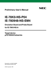
IE-780948-NS-EM4
User Manuals: NEC IE-780948-NS-EM4 Hardware Development
Manuals and User Guides for NEC IE-780948-NS-EM4 Hardware Development. We have
1
NEC IE-780948-NS-EM4 Hardware Development manual available for free PDF download: User Manual
NEC IE-780948-NS-EM4 User Manual (72 pages)
Emulation Board and Probe Board
Brand:
NEC
| Category:
Computer Hardware
| Size: 0 MB
Table of Contents
Introduction
5
Table of Contents
7
Chapter 1 General
11
System Configuration
12
Figure 1-1: System Configuration
12
Hardware Configuration
14
Figure 1-2: Basic Hardware Configuration
14
Basic Specifications
15
Table 1-1: Basic Specifications
15
Notes on Use of IE-78K0-NS-P04 and IE-780948-NS-EM4
16
Chapter 2 Part Names
18
Package Components
18
Parts of the IE-78K0-NS-P04
19
Figure 2-1: IE-78K0-NS-P04 External View and Part Names
19
Parts of the IE-780948-NS-EM4
20
Figure 2-2: IE-780948-NS-EM4 External View and Part Names
20
Table 2-1: Names of IE-78K0-NS-P04 and IE-780948-NS-EM4 Parts
21
Chapter 3 Installation
23
Installation Procedure
24
Figure 3-1: IE-78K0-NS-A Inside
24
Table 3-1: Flash ROM Mode
24
Table 3-2: Internal Mode 1
24
Table 3-3: Internal Mode 2
25
Table 3-4: Main Clock Selection
25
Table 3-5: Main Clock Doubler Selection
25
Table 3-6: Sub Clock Selection
25
Figure 3-2: Main Board (G-780009) Jumper Positioning
26
Table 3-7: FPGA Mode Selection (for Internal Tests Only)
26
Table 3-8: Ground Voltage Pin of AD-Converter
26
Table 3-9: VCC Voltage Pin of AD-Converter
27
Table 3-10: Voltage Setting
27
Table 3-11: Voltage Setting
27
Table 3-12: LED Indicator D1, D2, D3
27
Figure 3-3: Emulation Board (IE-78K0-NS-P04) Jumper Positioning
28
Table 3-13: User RESET Mode
28
Table 3-14: DCAN Transmit Buffer Selection
28
Figure 3-4: Probe Board (IE-780948-NS-EM4) Jumper Positioning
29
Table 3-15: DCAN Receive Buffer Type Selection
29
Table 3-16: LED Indicator D2
29
Figure 3-5: Connection of Boards
30
Clock Settings
31
Overview of Clock Settings
31
Figure 3-6: External Circuits Used as System Clock Oscillation Circuit
31
Main System Clock Selections
32
Figure 3-7: When Using Clock that Is Already Mounted on Emulation Board
32
Figure 3-8: When Using User-Mounted Clock
32
Subsystem Clock
33
Figure 3-9: When Using an External Clock
33
Figure 3-10: When Using Standard Clock Mounted on Main Board
33
Figure 3-11: When Using Clock Mounted on the Emulation Board
34
Figure 3-12: Using an External Clock Mounted on the Target Hardware
34
Main System Clock Settings
35
Table 3-17: Main System Clock Settings
35
Figure 3-13: Connections on Parts Board (When Using Main System Clock or User-Mounted Clock)
36
Figure 3-14: IE-78K0-NS-A Side (Emulation Device)
37
Figure 3-15: Crystal Oscillator (When Using Main System Clock or User-Mounted Clock)
38
Figure 3-16: Pin Alignment of Crystal Oscillator and Socket
38
Figure 3-17: IE-78K0-NS-A Side (Emulation Device)
39
Examples of Main System Clock Setting
40
Subsystem Clock
41
Subsystem Clock Setting
41
Table 3-18: Subsystem Clock Settings
41
Figure 3-18:Connections on Parts Board (When Using Subsystem Clock or User-Mounted Clock)
42
Figure 3-19: IE-78K0-NS-A Side
43
Figure 3-20: Crystal Oscillator (When Using Subsystem Clock or User-Mounted Clock)
44
Figure 3-21: IE-78K0-NS-A Side
45
Figure 3-22: IE-78K0-NS-A Side
45
Examples of Subsystem Clock Setting
46
LCD-C/D Resistor Network
47
Jumper Settings on IE-78K0-NS-A
48
Table 3-19: Jumper Settings on IE-78K0-NS-A
48
Table 3-20: Jumper Settings on IE-78K0-NS-P04
48
Table 3-21: Jumper Settings on IE-780948-NS-EM4
48
External Trigger
49
Figure 3-23: External Trigger Input Position
49
Chapter 4 Differences Among Target Devices and Target Interface Circuits
51
Input/Output Signals
52
Figure 4-1: Equivalent Circuit 1 from Emulation Circuit
53
Figure 4-2: Equivalent Circuit 2 from Emulation Circuit
54
Figure 4-3: Equivalent Circuit 3 from Emulation Circuit
55
Differences in Port Functions
56
Differences in SFR-Registers
56
Target Interface Circuit
56
Chapter 5 Restrictions
58
Appendix A IE-78K0-NS-P04, IE-780948-NS-EM4 Product Specifications
60
Appendix B Conversion Socket Adapter Package Drawings and Recommended Board Mounting Pattern
62
Figure B-1: 100GF Package Drawings (Reference)
63
Figure B-2: NQPACK100RB (Target Side) Package Drawings (Reference)
64
Figure B-3: YQPACK100RB (Probe Side) Package Drawings (Reference)
65
Figure B-4: HQPACK100RB (Tlid for Device Mounted) Package Drawings (Reference)
66
Appendix C Pin Correspondence Tables of Emulation Probe
68
Table C-1: Connector CN11 to Emulation Probe (1/2)
68
Table C-1: Connector CN11 to Emulation Probe (2/2)
69
Advertisement
Advertisement
Related Products
NEC IE-780338-NS-EM1
NEC IE-789026-NS-EM1
NEC IE-789306-NS-EM1
NEC IE-789860-NS-EM1
NEC IE-784915-R-EM1
NEC IE-784937-NS-EM1
NEC IE-789801-NS-EM1
NEC IE-789835-NS-EM1
NEC IE-784225-NS-EM1
NEC IE-784000-R
NEC Categories
Monitor
Projector
Server
Telephone
Computer Hardware
More NEC Manuals
Login
Sign In
OR
Sign in with Facebook
Sign in with Google
Upload manual
Upload from disk
Upload from URL