Sign In
Upload
Manuals
Brands
Honeywell Manuals
Transceiver
Bendix/King KX 165A
Honeywell Bendix/King KX 165A Manuals
Manuals and User Guides for Honeywell Bendix/King KX 165A. We have
1
Honeywell Bendix/King KX 165A manual available for free PDF download: Maintenance Manual
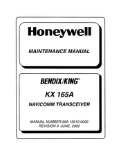
Honeywell Bendix/King KX 165A Maintenance Manual (297 pages)
NAV/COMM Transceiver
Brand:
Honeywell
| Category:
Transceiver
| Size: 6.07 MB
Table of Contents
Table of Contents
3
Theory of Operation
9
General
9
Kx 165A Features
9
Block Diagram Theory of Operation
10
FIGURE 4-1 KX 165A Block Diagram
10
Com Receiver
11
FIGURE 4-2 KX155A NAV/COM Receiver - Main Board Audio Circuitry
13
Transmitter
15
FIGURE 4-3 Transmitter Block Diagram
17
Vor/Loc Receiver
18
FIGURE 4-4 vor Signal Generation
20
FIGURE 4-5 Localizer Signal Generation
21
Glideslope Receiver
22
FIGURE 4-6 Glideslope
23
FIGURE 4-7 200-09447-000 KX 165A Glideslope Receiver Block Diagram
24
Central Processing Unit (Cpu)
25
FIGURE 4-8 CPU Block Diagram
26
Front Panel and Display
27
Power Supply
27
FIGURE 4-9 Front Panel and Display Diagram
28
FIGURE 4-10 Power Supply Block Diagram
29
FIGURE 4-11 VOR/LOC Converter Board Block Diagram
30
VOR/LOC Converter Board
30
Detailed Circuit Theory
32
Com Receiver
32
TABLE 4-1 Component Designators
32
Transmitter
36
Nav (Vor/Loc) Receiver
37
Table 4-2 Gs/Loc Frequency Pairs Vs. Gs Vco Frequency
40
GLIDESLOPE RECEIVER Fig 6-29
41
Cpu Function
44
Power Supply
46
Front Panel and Display Module
46
VOR/LOC Converter I/O Board
47
Maintenance
50
5.1 General Information
50
Standard Test Signal Description
50
5.2 Test and Alignment
51
Test Equipment
51
TABLE 5-1 Maximum Load Driving Capacity
51
Figure 5-1 Typical Test Equipment Setup
53
Figure 5-2 Bench Test Harness
55
FIGURE 5-2 Bench Test Harness (Sheet 2 of 2)
55
Unit Level Alignment
56
TABLE 5-2 Pages Accessed by Mode Button
56
TABLE 5-3 Alignment Data
68
Final Test Procedure
71
FIGURE 5-3 Audio Injection Circuit
86
FIGURE 5-4 Linear Detector
86
Overhaul
87
Visual Inspection
87
FIGURE 5-5 Elliptic Filter Tuning Injection Circuit
87
Cleaning
89
Repair
89
Kx 165A Disassembly
89
Software Updates
93
TABLE 5-5 KX 155A Mainboard Voltage Measurements
94
TABLE 5-6 KX 155A Nav/Com Receiver Test Voltages
95
TABLE 5-7 KX 155A Glideslope Test Voltages (200-09060-0000 Board)
98
FIGURE 5-6 Waveform Notes
99
Figure 5-7 Rcvr Bd Clock Waveform at P3001-3
100
Figure 5-8 Rcvr Bd Data Waveform at P3001-5
100
Figure 5-10 Rcvr Bd Enable Waveform at Enable Decoder
101
Figure 5-9 Rcvr Bd Data Waveform at P3001-4
101
Figure 5-11 Rcvr Bd Waveform at Tp 31 (Std Comm Input)
102
Figure 5-18 Rcvr Bd Waveform at Collector of Q15
105
Figure 5-20 Rcvr Bd Waveform at the Collector of Q23
106
Figure 5-21 Rcvr Bd Waveform at U15 Pin 12 Tp5
107
Figure 5-24 Rcvr Bd Waveform Junction of Q16 and R172
108
Figure 5-27 Rcvr Bd Waveform at Tp2
110
Figure 5-28 Rcvr Bd Waveform at U13 Pin 14( no Rf Applied)
110
Figure 5-30 Rcvr Bd Waveform at Tp30
111
Figure 5-31 Rcvr Bd Waveform at U23 Pin 12 (Tp9)
112
Figure 5-88 Main Board Waveform at J4 Pin 8 During Transmit
141
Figure 5-89 Main Board Waveform at J4 Pin 1 During Reception
141
Figure 5-90 Main Board Waveform at Q38 Emitter During Transmit
142
Figure 5-91 Main Board Waveform at Q38 Emitter During Reception
142
Figure 5-92 Main Board Waveform at J4 Pin 2 During Transmit
143
Figure 5-93 Main Board Waveform at J4 Pin 2 During Reception
143
Figure 5-94 Main Board Waveform at U28 Pin 4 During Transmit
144
Figure 5-95 Glideslope Waveform at the Base of Q4
144
Figure 5-96 Glideslope Board Waveform at Tp4
145
Figure 5-99 Glideslope Board Waveform at the Junction of R89 and R91
146
Figure 5-100 Converter Bd Waveform at Tp9
147
Figure 5-101 Converter Bd Waveform at Tp9
147
Figure 5-102 Converter Bd Waveform at Tp9
148
Figure 5-103 Converter Bd Waveform at Tp9
148
Illustrated Parts Lists
149
Bill of Material Description
149
Introduction
149
Software Documentation
152
FIGURE 6-1 Sample Parts List
155
FIGURE 6-2 Final Assembly
161
FIGURE 6-3 Bezel Assembly
165
FIGURE 6-4 Bezel
168
FIGURE 6-5 Front Panel Assembly
173
FIGURE 6-5 Front Panel Assembly
174
FIGURE 6-6 Front Panel Schematic
176
FIGURE 6-7 KX 165A Main Board Assembly
197
FIGURE 6-7 KX 165A Main Board Assembly
198
FIGURE 6-8 KX 165A Main Board Schematic
201
FIGURE 6-8 KX 165A Main Board Schematic
202
FIGURE 6-8 KX 165A Main Board Schematic
203
FIGURE 6-8 KX 165A Main Board Schematic
204
FIGURE 6-8 KX 165A Main Board Schematic
205
FIGURE 6-8 KX 165A Main Board Schematic
206
FIGURE 6-9 TX Audio Adapter
214
FIGURE 6-10 TX Audio Adapter Schematic
215
FIGURE 6-11 Base Assembly
218
FIGURE 6-12 Transmitter Board
223
FIGURE 6-13 Transmitter Schematic
225
FIGURE 6-14 RF Pwr Transistor Assembly
228
FIGURE 6-15 Transmitter Filter Board
232
FIGURE 6-16 Transmitter Filter Board Schematic
233
FIGURE 6-17 Directional Coupler
236
FIGURE 6-18 Directional Coupler Schematic
238
FIGURE 6-19 COM/VOR Receiver Board
253
FIGURE 6-21 COM/VOR Receiver Board Schematic
262
FIGURE 6-22 if Filter Board
269
FIGURE 6-23 if Filter Board Schematic
270
FIGURE 6-24 Top Cover Assembly
273
FIGURE 6-25 VOR/LOC Converter Board
278
FIGURE 6-26 VOR/LOC Converter Board Schematic
279
FIGURE 6-27 Glideslope Assembly
283
FIGURE 6-28 Glideslope Board
290
FIGURE 6-29 Glideslope Board Schematic
291
Advertisement
Share and save
Advertisement
Related Products
Honeywell Bendix/King KY 196B
Honeywell BENDIX/KING KY 96A
Honeywell BENDIX/KING KY 97A
Honeywell Bendix King Silver Crown Plus KX 155A
Honeywell Bendix King Silver Crown Plus KX 165A
Honeywell KXP2290
Honeywell Bendix/King KMD 550
Honeywell Bendix/King KRA 405B
Honeywell KFC 150
Honeywell BENDIX/KING KCS55
Honeywell Categories
Thermostat
Controller
Control Unit
Security Camera
Accessories
More Honeywell Manuals
Login
Sign In
OR
Sign in with Facebook
Sign in with Google
Upload manual
Upload from disk
Upload from URL